Note: Descriptions are shown in the official language in which they were submitted.
CA 02334517 2000-12-07
WO 00/00335 PCT/US99/12848
FABRICA7CION OF THREE-DIMENSIONAL OBJECTS
Reference to Government Grant
This invention was made with Government support under Contract Number N00014-
95-
C-0019, awarded by the Office of Naval Research. The government has certain
rights in this
invention.
Technical Field
The present invention relates generally to automated layered production of
three-
dimensional objects.
1o Background
Conventional techniques for mass producing three-dimensional objects typically
include
casting, deforming, machining and assembling. While such techniques axe
capable of producing
complicated objects in high volume at relatively low cast, they are often
poorly adapted for rapid
prototyping, and for relatively short production runs.
15 Direct CAD Manufacturing systems (DCM) are somewhat better adapted to rapid
prototyping. In DCM systems computers are employed to produce a three-
dimensional model of
a desired object, and then to drive servo-mechanisms which produce the desired
object. This
generally involves machining or application of other subtractive processes on
a starting block of
material. Subtractive DCM leas proven to be cost effective in automotive,
aerospace, appliance,
zo .toy manufacturing, and marry other industries that involve repeated design
and prototyping of
parts. Such systems, however, are not well suited to producing prototypes
having complicated
internal construction. This is a natural function of starting the process with
a substantially solid
block of material, and machining the part from the outside.
Additive DCM systems address this problem by producing a three-dimensional
object
z5 from a large number of individual layers. The layers can be machined in the
normal fashion aid
then pinned, welded or otherwise held l:ogether, or they can be deposited one
on top of the other
through deposition of a flowable build material. The latter systems are
generically referred to
herein as Solid Freeform Fahrication (SFF) systems.
In SFF systems each layer is typically only about 0.1 to 0.25 mm. thick. This
provides
3o about 40 to 100 layers far each cm of object, and allows SFF systems to
produce objects having
complicated internal structure. While SFF systems may not yet be able to
produce objects
CA 02334517 2000-12-07
WO 00/00335 PCT/US99/12848
2
having exactly the same shape achievable with other methods, they are
generally able to produce
"near net shape" objects, i.e., those having substantially the end-shape
desired, and which can
then be readily finished by conventional processing steps. For convenience in
the descriptions
herein, the term "object" is employed to mean both the final object and any
intermediate near net
shaped object. In a similar manner, the terms "fabricate" and "fabricating"
are used herein to
include both production of a f n,al product from a starting material, and
production of a
recognizable intermediate. Thus, a "method for fabricating a three-dimensional
object" may
involve merely producing an inl:ermediate that is visibly similar to the
finished object or product,
but which requires additional processing to arrive at the finished object or
product.
1o In addition to producing fairly complicated objects, SFF systems may
advantageously
employ multiple deposition heads to deposit a plurality of different
materials. US Pat. Nos.
4,999,143 and 5,569,349 (Oct. 1996) to Almquist et al., for example, describe
depositing both a
build material and a supporting material in a series of layers. Moreover,
while there is little or no
enablement in this area, it has a?Eso been suggested that different build
materials can be employed
15 within a single layer to produce an electrically conductive path.
In SFF systems it is generally desirable to harden or otherwise cure the
flowable build
material deposited at each layer according to a pattern that matches a
corresponding cross-
section of the object being produced. While numerous different systems and
methods have been
proposed, there are conceptually only two classes of methods for hardening the
layers in
2o predetermined patterns -- selective deposition and selective curing. In
selective deposition
methods, the build material is laid down from the outset in the desired
pattern, and then typically
cured via cooling or polymerization. Suitable apparatus for this class of
methods necessarily
involves some sort of delivery dispenser that is moveable with respect to the
rest of the build.
Examples of such delivery dispensers are the extrusion head of US Pat. No.
4,749,347 to
25 Valavaara, and the droplet emitting head of US Pat. No. 4,665,492 to
Masters.
In selective curing methods, the build material is deposited across an entixe
surface, or
throughout an entire volume, and then energy is imparted to selected portions
of the build
material to produce the desired pattern. At some point in the process the non-
cured material is
then washed or brushed away. l;.ight energy is typically employed to produce
the desired pattern,
3o and many extant systems employ one or more laser beams to trace out the
desired images in the
CA 02334517 2000-12-07
WO 00/00335 PCTJUS991128~t8
3
deposited build material. Lasers have been employed in this manner for Iaser
sintering of build
materials containing a metal, a metal containing powder, or a plastic; as
described in US Pat. No.
4,752,352 to Feygin, 4,863,538 to Deckard, and 4,938,816 to Bearnan et al. It
is also known to
apply light energy to the deposited. build material in a pattern that
corresponds to an entire cross-
sectional image. This method is g~~neraily referred to as sterolithography,
and various
embodiments are described in U.S. Patent Nos. 4,929,402 and 5,236,637 to Hull,
and US Pat.
Nos. 4,961,154 and 5,031,230 to F'omerantz et al.
In the last several years advances in SFF systems have driven a demand to
provide
functional properties in SFF produced objects that are comparable to those of
conventionally
1~ produced objects. Among other tlungs, manufacturers have expressed a desire
to provide SFF
produced objects that have the strength and crack resistance approaching that
of forged metal
components. A desire has also been expressed to provide SFF objects that
include conducting
paths, such as electrical, thermal or magnetic conduction paths.
Sinterable metals, alloys and ceramics can be used to produce f nal products
having
15 excellent structural strength, (see e.g., U.S. Patent No. 5,496,892 to
~uadir et ai., and 4,906,424
to Hughes et al.). But these materials are generally unsuitable as build
materials in SFF systems
because they become fluid only at high temperatures or pressures. This creates
considerable
difficulties in handling and deposition, among other things by limiting the
rate at which new
layers can be applied to a build. T'he problem can be resolved to some extent
by ejecting small
2o particles or droplets from a dispenser rather than extruding relatively
larger masses, but
operating conditions are still severe, and generally unsuited for many
applications. The problem
can be resolved somewhat further by using an electrorheological support during
the deposition
process, as taught in US 5,362,42',1 to Mitchell (Nov. 1994), but that
solution adds yet additional
complications. In any event, the extreme deposition conditions presently
required for depositing
25 metal and alloy build materials in SFF systems largely preclude the
inclusion of plastics or other
materials during the build process, which all but eliminates the inclusion of
many desirable
functional properties in SFF products.
Metal containing powders such as aluminum oxide, zirconium silicate, fused
silica, and
silicon carbide are relatively easy to deposit, such as by the slurry droplet
method of US Pat. No.
30 4,655,492 to Masters (May 1987)" but are difficult to bind together to
provide adequate strength.
CA 02334517 2000-12-07
WO 00/00335 PCTIUS99/12848
4
Among other things cracking is a serious problem. Low temperature sintering
can be used to
ameliorate this problem to some extent, but requires inordinate amounts of
time. High
temperature sintering can also be 'used, but requires difficult or adverse
conditions, and is only
moderately effective. Binders can also be used to increase inter-particle
strength, as described in
US Pat. No. 5,660,621 to Bredt (Aug. 1997), but SFF processes using extant
binders still tend to
provide only relatively weak structures.
Polymerizable build materials are easier to handle and deposit, but generally
provide
poor structural strength. Such materials are also not known to provide the
many functional
qualities that may be desired. In addition, the form energy used to initiate
polymerization may
itself be problematic. Many photopolymers, for example, utilize UV radiation
which can cause
injury. Still further, the time required for the photopoiymers to solidify
upon exposure to UV
radiation can be prohibitively long, thereby inordinately increasing the build
time. .
Waxes, thermosetting and thermoplastic materials, two-part epoxies, foaming
plastics,
and glass have also all been used in conjunction with SFF. These materials,
however, are
s usually quite weak, and suffer from many of the same problems described
above.
Thus, there is still a need tto provide novel build material compositions and
methods for
use in the solid free-form fabrication of three-dimensional objects.
Summary of the Invention
The present invention provides compositions and methods for use in the
stepwise, layer
zo by layer fabrication of three-dime;nsianal objects, in which a build
material contains a metal
having a covalent bond to a non-metal, and the layers are processed to produce
the three-
dimensional object at least in part through a chemical reaction which alters
the covalent bond of
the metal.
In a first major class of preferred embodiments, the build material includes a
metal that is
25 covalently bound to a polymeric precursor. The precursor is polymerized;
and at least some of
the non-metallic component of tine polymer is burned away, or otherwise
removed during
subsequent processing in such a manner that the covalent bond of the metal is
broken. In more
preferred embodiments of this cl;~ss, a Iigand is also bound at some point to
the polymer or a
polymer precursor, both the metal and the Iigand are freed during the
subsequent processing, and
3o the metal becomes bound to the Iigand.
CA 02334517 2000-12-07
WO 00/00335 PCT/US99/12848
In another major class of preferred ernbodiments, the build material includes
a metal,
Me, that is covalently bound to a :first ligand, L1. Following deposition of
the build material, the
first ligand undergoes a redox reaction with a second Iigand, L2, thereby
breaking the covalent
bond of the metal. In more preferred embodiments of this class, Ll and LZ
react to form a gas,
and the metal reacts to form an oxide such as MeSOX, MeNOX, MeCOX and so
forth. In still
more preferred embodiments the .build matexial includes several metal species
that ate covalently
bound to ligands, giving rise to several redox reactions and producing mixed
metal products.
In yet another aspect of the invention., multiple build materials are employed
in building
the three-dimensional object. The various build materials are selected and
deposited in a manner
3o which produces functional non-uniformities. Preferred non-uniformities
include electrical,
thermal, and magnetic conduction paths, structural supports, chemical and wear
resistant areas,
and so forth.
Various objects, features, aspects and advantages of the present invention
will become
more apparent from the following detailed description of preferred embodiments
of the
15 invention, along with the accompanying drawings.
Brief Description of the Figure;
FIG. 1 is a block diagram of a method for fabricating a three-dimensional
object
according to a selective curing aspect of the present invention.
FIG. 2 is an illustration of a system by which a three-dimensional object can
be
2o fabricated in accordance with the method of FIG. 1.
FIG. 3 is an illustration of an alternative system by which a three-
dimensional object can
be fabricated in accordance with 'the method of FIG. 1.
Detailed Description
The practice of the present invention can employ, unless otherwise indicated,
25 conventional techniques of photochemistry, ceramic chemistry, polymer
chemistry, and rapid
prototyping and manufacturing that are within the skill of the art. See, e.g.,
Kirk, Encyclopedia
of Chemical Technology, Burns automated Fabrication (PTR Prentice Hall,
Englewood Cliffs,
NJ (1993)), and Jacobs, Rapid Prototyping and Manufacturing: Fundamentals of
Stereolithography (Society of Manufacturing Engineers, Dearborn, MI (1992)).
All patents,
CA 02334517 2000-12-07
WO 00100335 PCT/US99/12848
6
patent applications, publications and other types of references cited herein,
whether supra or
infra, are hereby incorporated by reference in their entirety. Despite the
incorporation of
references, the present text does riot necessarily adopt the definitions and
usages set forth in the
references. Therefore, to clarify the definitions and usages of specific terms
that are not defined
elsewhere herein, we set forth the following.
The singular forms "a," "a~n" and "the" are used herein to include the plural
unless the
content clearly dictates otherwise. Thus, for example, reference to "a ceramic
powder" includes
mixtures of such powders, reference to "a polymerizable monomer'°
includes more than one such
monomer, reference to "a layer" includes more than one layer, and the like.
l0 The term "three-dimensional object" is used herein to mean any structure
that
substantially retains its intended i:unction and shape when removed from an
external support.
Thus, a thin film such as that deposited on a piece of glass is generally
considered herein not to
be a three-dimensional object because it tends to lose its intended
functionality and/or shape as it
chips or peels away from the glass. A thick f im such a sheet of aluminum
foil, on the other
15 hand, is considered herein to be a. three-dimensional object because it
retains its shape and
function long after it is removed :From any roller or other external support
employed during its
production.
The term "CAD" is used Therein in its broadest sense to include all manner of
computer
aided design systems, including pure CAD systems, CAD/CAM systems, and the
like, provided
2o that such systems are used at least in part to develop or process a model
of a three-dimensional
object.
The term "build material''' is used herein to mean any material that is
deposited in a layer-
by-layer fashion to construct the three-dimensional object. This definition
expressly excludes
structures that are not added in a layer-by-layer fashion, such as central or
peripheral supports
25 that may be incorporated during come aspect of the fabrication process. As
taught herein,
multiple build materials may be included in the fabrication of a single three-
dimensional object,
to form support structures, conductive paths, and so forth.
The term "metal" is used herein to mean an element selected from one of the
metal and
transition metal groups of the periodic table. Since metals can be present in
many different
CA 02334517 2000-12-07
WO 00/00335 PCT/US99/12848
7
forms, however, the form of the element is determined by the context. Thus,
when referring to
"metals and alloys", the term metal means a composition consisting
substantially of metal and
transition metal elements. When refernng to "metal and alloy composites", the
term metal
means a composition consisting substantially of one or more metal and
transition metal
elements, along with some non-metallic composition such as a ceramic. When
referring to
metals having a covalent bond, the term metal means an element selected from
one of the metal
and transition metal groups, and which is covalently bound to a non-metal.
The term "covalent bond" is used herein to mean any chemical bond other than a
purely
ionic bond. Covalent bonds thus include ordinary organic bonds such as the
carbon-hydrogen
1 o and carbon-oxygen bonds in a sugar, and also include the metal-Iigand
bonds in a coordination
complex, such as NiCI2 (pyridine:)4.
The term "successive Iaye:rs" is used herein to mean layers of build material
which are
sequentially deposited on a build. It is not necessary that a previous Iayer
be completely
solidified or otherwise cured before the subsequent layer is added, and indeed
it is generally
15 advisable that the subsequent layer is added before the previous layer is
fully cured. This
improves inter-layer bonding. On the other hand, if a layer of build material
is deposited on the
build, and then additional build material is added before any substantial
curing of the previously
deposited material takes place, then both the previously deposited and
additionally deposited
build material are considered herein to comprise the same layer.
2o The term "cross-sectional pattern" is used herein to mean a representation
of a cross-
section of the object being built. Generally speaking, the cross-sectional
pattern will be a
complete vertical cross-section, because most builds are contemplated to be
produced one
complete layer at a time, in a vertical, stepwise fashion. Nevertheless, it is
also contemplated
that partial cross-sections could be employed, such as to accommodate
different build materials.
25 In addition, it is contemplated that non-vertical cross-sections could be
employed, so that the
object being build would be constructed sideways, or in same other non-
vertical manner. Non-
vertical builds might, for example, be employed advantageously to provide
extra strength in a
particular direction.
"Visible light" is electromagnetic radiation with wavelengths ranging from 4 x
103 A to
3o about 7.7 x 10³A. "Near infrareds light" or "near IR light" is
electromagnetic radiation with
CA 02334517 2000-12-07
WO 00/00335 PCT/US99/12848
wavelengths ranging from 7.5 x 1103 A to about 30 x 103 A. "Actinic radiation"
is radiation
capable of initiating photochemic;al reactions.
Turning now to FIG. 1, a flow chart illustrates steps that may advantageously
be used to
produce a three-dimensional object using SFF techniques according to the
present invention. In
step 1, a computer representation or "model" of the object to be formed is
generated using a
CAD/CAM software system. The software then preferably generates an STL file,
and the STL
file is converted into "slice" data corresponding to vertical cross-sectional
patterns of the object.
Of course, the CAD model need :not be a perfect representation of the object,
and the slice data
and cross-sectional patterns need not be perfect representations of the CAD
model. Instead,
l0 each of these need only be "derived" in part from its source. It is
particularly contemplated, for
example, that dimensions may be; scaled to produce a scaled-up or scaled-down
product, or to
compensate for shrinkage or other processing factors. As another example, it
may be preferable
to compensate for the change in distance from the light source to the
uppermost layer of build
material as the build grows by modifying the projected image, rather than
moving either the
15 build or the light source.
In step 2, a layer of a photopolymerizable build material is applied to either
a work
surface or to a previous layer. The build material is leveled to a desired
thickness that
corresponds to the thickness of the "slice" generated by the computer. At
least one build material
employed in all contemplated embodiments of the present invention includes a
metal having a
2o covalent bond to a non-metal.
It is particularly contemplated that multiple build materials may be employed
in a given
layer, or different build materials employed from layer to layer. This may be
accomplished
using multiple deposition heads" or a single deposition head through which
multiple materials
flow. Manifolds which can be used for this purpose are known in the art.
25 Presently preferred build materials suitable for the bulk of the product
being produced
include polymerizable silazane, silane, borazine, borane oligomers, and other
preceramic
monomers, oligomers, or polymers functionalized by polymerizable groups (e.g.,
vinyl, acrylate,
methacrylates, and so on); metal acrylates, metal methacrylates and other
polymerizable metal
carboxylates; metal carboxylate in the presence of oxidizing species and metal
nitrates in the
3o presence of reducing species. Such materials are selected because of their
ability to be
CA 02334517 2000-12-07
WO 00/00335 PCT/US99/12848
9
chemically transformed into ceramics, such as metal nitrides, carbides or
oxides, or metals by
heating and for some of them, because of their ease of polymerization. These
build materials
may or may not be used in combination with other curable monomers or
oligomers. Among
other suitable build materials, it is contemplated that copper formate and
gold acetate-
s isobutyrrate would be particularly well suited for providing an electrical
conduction path, silver
acrylate and Pd(CHOCOO)(CH20HCOO) would be particularly well suited for
providing a
thermal conduction path, silizan~a and silanes would be particularly well
suited for providing
structural support, and zirconiwr.~ and aluminum acrylates would be
particularly well suited for
providing barrier coatings and a surface compressive stress layer.
Additionally, layers containing
1 o these and other materials may advantageously have different coefficients
of thermal expansion
than other layers.
In step 3, appropriate slice data from step 1 is fed to a selective
photoexposure device,
which in turn exposes the layer of build mal:erial deposited in step 2 with a
suitable actinic
radiation according to the corresponding cross-sectional pattern derived from
the CAD model.
15 Here again, it should be cautioned that a perfect correlation between the
exposure pattern and the
computer generated cross-sectional pattern need not be followed. Hence, the
term "according to
the corresponding cross-sectional pattern" includes both more and less
accurate correiations
between the exposure pattern and the corresponding cross-sectional pattern.
Appropriate intensity and duration of the exposure is contemplated to be
established
2o experimentally. Nevertheless, it :may be understood that suitable values
for these parameters will
vary as a function of numerous factors, including the nature of the monomers
or other
polymerizable material, the amount and activity of the photoinitiator, and the
thickness and
transparency of each layer to the radiation. Our experiments have demonstrated
that it is
desirable for each layer to be caved to a tacky point before adding the next
sequential layer. This ,
25 provides a suitable hardness, while still perimitting adequate bonding
between adjacent layers.
Specific exposure parameters are given below, but in general it is
contemplated that intensity
will be about 20 rnW per cm2 at the surface of the uppermost layer, and that
intensity will be
maintained for about five seconds to about sixty seconds.
The selective photoexposure device preferably comprises a DLP or LCD desktop
3o projector. Alternatively, the selective photoexposure device comprises a
source of actinic
CA 02334517 2000-12-07
WO 00/00335 PCT/US99/12848
radiation and a computer generated mask displayed on an LCD panel, that allows
actinic
radiation to pass therethrough in .areas corresponding to areas of the
photopolymerizable build
material to be solidified. The mask blocks the passage of radiation from areas
of the layer not to
be solidified. In yet a different embodiment, the selective photoexposure
device comprises
scanning layer optics.
In step 4, the build material is polymerized upon exposure to the actinic
radiation to form
a polymer having shaped according to the corresponding computer-generated
cross-sectional
pattern. In step 5, steps 2 through 4 are repeated to gradually build up the
object desired.
Depending on the number of IayE;rs the entire process may take several hours,
or even several
I o days, and may involve up to 5,000 layers or more.
In step 6, the object is removed from the build apparatus and heated to remove
at least a
large percentage of the organics. Heating may take place in a standard
processing oven, or may
occur in an alternative oven such. as a microwave oven. In general, it is
contemplated that the
object will be heated to between about 100° C and about 350° C,
for between about a few
I s seconds and about 48 hours. Once again, the temperature and heating period
rnay be derived
experimentally. During heating it is contemplated that the covalent bonding of
at Ieast one
species of metal in at least one build material will be broken, A new covalent
bond involving
the metal may or may nat be formed. For example, build material such as
Pd{CHOCOO)(CHZOHCOO) decomposes at 350° C leaving a relatively pure
form of palladium
2o metal. In contrast, build material such as
CH3 CH=CH2
--E ~ iNH~ ~ iNH~
H H
and the correspondent polymer are burned at about 450°C to 550°C
to drive away the organics of
such polymers, leaving a relatively pure form of silcon nitride, and build
materials such as lead
acetate, zirconium nitrate, and titantium acetylacetonate, which decomposes
between about
2s 350°C and about 600°C, leaving a relatively pure form of lead
zirconate titanate.
CA 02334517 2000-12-07
WO 00/00335 PCTIUS99112848
11
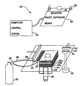
FIG. 2 illustrates a preferred embodiment of a device 20 suitable for
implementing the
method illustrated and described. in the flow chart of FIG. 1. Device 20
generally comprises a
work surface 22 having a build table 24 vvith a superior face 26 that can be
displaced vertically
by way of an elevator 28, e.g., a stepper motor, or the like. A
photopolymerizable build material
30 is dispensed onto work surface 22 from, for example, pressurized tank 32,
through valve 33
and then through suitable ports ~t4 in the work surface. Alternatively, the
build material 30 may
be routed through valve 33 to conduit 36 and directly to work surface 22. The
photopolymerizable composition 30 is applied over the work surface to a
predetermined
thickness by a leveling means 3l3, e.g., a doctor blade, to form layers 40a,
40b, and 40c on build
to table 24. A typical layer thickness ranges between 1 mil to 25 mil,
preferably between 1 mil to
mil. Excess material is optionally removed by action of recovery means 42,
e.g., a
"squeegee," through drain 44 intro recovery vat 46. The Leveling means is then
raised and vertical
positioning means 48, e.g., a pneumatic cylinder, lowers selective
photoexposure device 50 held
in frame 52. The layer of photopolymerizable composition 30 is selectively
exposed to actinic
radiation by activating selective photoexposure device 50. Any uncured
material is removed,
e.g., by aspiration. A solvent, e.g., hexane, acetone, or the like, may be
used as an aid to dislodge
the uncured material.
Selective photoexposure device 50 :preferably comprises a digital micromirror
device
("DMD") for DLP projector or m LCD projector. Such projectors are designed to
interface with
2o CAD/CAM and STL slice conversion software. The slice information is
converted to a cross
section image of the layer and light is projected corresponding to those areas
of the layer to be
photopolymerized. The image projected by the DLP or LCD projector is
controlled by computer
system 54. DMD for DLP projectors may be obtained, for example, from Proxima
(Desktop
Projector Model 4100) or InFocus Systems (Lite Pro 620). LCD projectors may be
obtained
from Proximal {Desktop Projector Model 240) or InFocus Systems (Lite Pro 2I0).
In another embodiment (not shown), the selective photoexposure device
comprises a
source of actinic radiation, an LCD panel that serves as an electronic mask,
and optical elements
as needed to collimate, focus, filter, or otherwise process the radiation that
passes through the
mask as required. Those skilled in the art vvill recognize that the optical
elements may include
various lenses, mirrors, filters, and the like, depending on the source of
radiation and the nature
of the photopolymerizable build material. The data corresponding to the two-
dimensional cross
CA 02334517 2000-12-07
WO 00100335 PCT/US99/12$4$ -
I2
section of the layer is fed to the L,CD panel to create an electronic mask,
through which actinic
radiation passes to solidify selected areas of the photopolymerizable
composition as discussed
above. The ability of the LCD panel to pass or block the passage of the
radiation is controlled by
computer system S4. The LCD panel may be one having an active or a passive
matrix screen.
LCD panels that may be used wirth the layer-by-layer photofabrication system
disclosed herein
are commercially available from., e.g., nView Model 2310 {nView, Newport News,
VA).
In FIG. 3, selective exposure device SO' comprises an optical system for laser
scanning.
A description of an exemplary optical system for laser scanning may be found
in Fisli (1983)
Proc. SPIE Int'1 Soc. Optical Eng;: 390:45-48. Preferably, system SO' is
affixed to leveling means
38 in a manner such that as the photopolymerizable build material is applied
over the work
surface to a predetermined thickness by the leveling means, the optical system
is translated over
the surface o f the layer of photo;polymerizable build material. The optical
system for laser
scanning SO' is loaded with an image of a cross section of the layer to be
fabricated from
computer S4. The image stored in the laser printer optics system is fed to the
laser which serves
to selectively expose the compo:cition to radiation, and thereby solidifies
those areas of the
composition corresponding to the cross section of the object to be formed. The
laser is
preferably a solid state diode laser which can be used to generate actinic
radiation in the neax
infrared spectrum or, with the us,e of a frequency doubter, in the visible
spectrum. Optical
systems for laser scanning are available from Xerox Corp. {Palo Alto, CA).
Solid state lasers
2o that emit in the visible or near IF: spectral ranges are available from
SDL, Inc. (San Jose, CA) or
Uniphase (San 3ose, CA).
A suitable source of actinic radiation is a visible light source or a near
infrared light
source. The visible light source may be a tungsten-halogen lamp, a xenon arc
lamp, e.g., Oriel
1000 Xenon arc lamp, or a visible solid state laser. Near infrared light
sources include solid state
diode lasers, quartz tungsten-halogen lamps, and the like.
Computer system S4 is used to generate a three-dimensional model of the object
to be
fabricated. The computer-generated model may be constructed on the computer
itself, using
CAD/CAM software. In the alternative, the model may be generated from data
scanned into the
computer from a prototype or from a drawing. The computer is thus used to
provide slice
3o information about the various layers of the object and to provide cross
section data for each layer
CA 02334517 2000-12-07
WO 00/00335 PCT/US99/12848
13
that is fed to selective photoexposure device S0. The computer-generated slice
information may
be provided to selective photoexposure device 50 at any time prior to exposure
of the
photopolymer to the radiation. Guidance for the selection of appropriate
CAD/CAM-and slice-
conversion software may be fownd in Jacobs (1992), supra, chapters 5 and 6,
and Burns (1993),
supra chapter 6.
Computer system 54 may be any system that is capable of modeling the object to
be
fabricated, slicing the model into layers having predetermined thickness and
providing two-
dimensional cross section data about the layer to selective exposure device 50
or the optical
system for laser scanning. Examples of uch systems have been described in U.S.
Patent No.
l0 4,961,154, supra, U.S. Patent No. 5,182,715 to Vorgitch et al., the
disclosure of which is
incorporated herein by reference;. CAD/CAM software is available from a number
of vendors
including, e.g., EDS-Unigraphic,s (Troy, MI), Structural Dynamic Research
Corporation
(Milford, OH), Hewlett-Packard, Mechanical Division (Ft. Collins, CO),
Autodesk (Sausalito,
CA). STL conversion software for rapid prototyping is available from vendors
such as Brock
15 Rooney and Associates (Birmingham MI), Irnageware (Ann Arbor, MI), Solid
Concepts, Inc.
(Valencia, CA), POGO International, Inc. (College Station, TX), and the like
Computer system
54 may perform a variety of functions in addition to generating the three-
dimensional model of
the object to be fabricated, the slice information about the layers of the
object, and the cross
section data for each layer, from which the mask is generated. Computer system
54 may be used
20 to control the operation of elevator means 28, valve 33, vertical
positioning means 48, and the
like.
When exposure of a layer is complete, selective photoexposure device 50 is
returned to
an elevated position to allow the application of a new layer of
photopolymerizable build material
to enable communication of data to the selective photoexposure device for
generation of the
25 cross section image of the succf;ssive layer. A three-dimensional object is
accordingly produced
by the step-wise buildup of layers, such as 40a, 40b, and 40c, on build table
24.
The build table 24 is used to support and hold the object during fabrication,
and to move
the object vertically as needed. Typically, after a layer is formed thereon,
the build table is
moved down so a fresh layer of photopolymerizable build material may be
applied over the just-
3o formed layer. Elevator means 28 can advantageously be capable of programmed
movement at an
CA 02334517 2000-12-07
WO 00/00335 PCT/US99/12848
14
appropriate speed with appropriate precision. The elevator means movement
mechanism may be
mechanical, pneumatic, hydraulic, or electric, and may include optical
feedback to control its
position relative to the work surface.
The photopolymerizable component of a photopolymerizable build material may
include
any uncured liquid, semi-solid or solid that c;an be cured by actinic
radiation, e.g., by visible .
light, near infrared light, or the like. Examples of such curable liquids,
semi-solids and solids are
disclosed in UV Curing: Science and Technology, Pappas, ed., Technology
Marketing Corp.
(Norwalk, CT), and Roffey, Photopolvmerization of Surface Coatings, J. Wiley &
Sons
(Chichester). Photopolymerizable resins are commercially available from, e.g.,
Applied Polymer
to Systems, Inc. (Schaumberg, IL), Ciba Geigy Corp. (Los Angeles, CA), UCB
Chemical Carp.,
Inc. (Srnyrna, GA), E.I. Du Pont de Nemours & Co. (Wilmington, DE) and
Sartomer (Exton,
PA}.
The polymerizable component may be a monomer, mixture of monomers, an
oligorner,
mixtures of oligomers, or a mixture of oligomers and monomers, which can be
polymerized and
1 S solidified by exposure to actinic :radiation such as near infrared ar
visible light. Suitable
photaactive monomers include acrylates, including mono-, di- and tri-
acrylates, and mixtures
thereof, methacrylates (see, Tu, in UV Curing Science and Technology, Pappas,
ed., supra,
Chapter 5), epoxides, or epoxide-acrylate formulations, and other visible ar
near infrared light
curable monomers. Examples include 2hydroxyethylacrylate,
hexanedioldiacrylate,
2o triethyleneglycoldiacrylate (''TEGDA") diethyleneglycoldiacrylate,
tetraethyleneglycoldiacrylate, trimethylolacrylate, and the like.
In one embodiment, a sol'~,id or semi-solid photopolymerizable build material
may be
formulated from a photopolymerizable monomer, or oligomer, ar both, mixed with
a polymer
that is optionally functianalized to have moieties with which the monomer or
oligomer may
25 react. Alternatively, the monomer, aligomer, or both may be mixed with a
wax. Preferably, the
monomer is an epoxide, e.g. Uvc~cure 1500 (UCB Chemical Carp.), 3,4-epoxycyclo-
hexylmethyl-3,4-epaxycyclohexane carboxylate (Aldrich), or 1,4-
butanedioldiglycidylether
{Aldrich), or an epoxyacrylate such as Ebecryl0 3200 (UCB Chemical Corp). More
preferably,
the monomer is an epoxide-acrylate blend. The oligomer may be a polyester-
acrylate oligomer,
3o such as, Ubecryl~ 438, Ubecryl~ 584, or Ubecryl~ 2047. Examples of waxes
that may be
CA 02334517 2000-12-07
WO 00/00335 PCT/US99/12848
incorporated into the photopolynnerizable build material include paraff n
waxes, microcrystalline
waxes, carnuba wax, mineral wax, synthetic waxes, such as polyethylene waxes,
and the like
(see, Encyclopedia of Polymer Science and Engineering, 2nd ed., vol. 17, pages
784-795).
A semi-solid or solid photopolymer composition is preferably dispensed onto
the work
table as a hot liquid. As the liquid cools it solidifies. The solidified
composition is photo-
polymerized by exposure to an appropriate wavelength of actinic radiation.
When a solid or
semi-solid photopolymerizable 1>uild material is used, additional support
components or
structures may or may not be designed into the object.
The photopolymerizable build material may also include a plasticizing solvent.
Solvents
1o having plasticizing properties include dibutylphthalate ("DBP"),
benzylbutylphthalate, other
phthalates, linear or cyclic carbonates such as propylene carbonate and
ethylene carbonate,
ketones such as cyclohexanone, methylethylketone, and higher homologs, ethers,
and the like.
Additional optional components that can be included in the photopolymerizable
build material
may be found in U.S. Patent No. 4,906,424 to Hughes et al. Optionally, a light-
sensitive additive
I5 is incorporated into the photopolymerizable build material to reduce the
energy necessary to
effect photopolymerization. Visible light photoinitiators are generally
multicomponent systems
including, e.g., a xanthene dye, .a first cainitiator such as an iodonium
salt, and a second
coinitiator. Suitable visible-near IR photoinitiators are described in U.S.
Patent Nos. 5,451,343
to Neckers et al., 5,395,862 to rleckers et al., 4,952,480 to Yamaguchi et al,
and 4,772,530 to
2o Gottschalk et al., De Raaff et al. {1996) RADTECH Conference Proceedings,
Chatterjee et al.
{1988) J. Am. Chem. Soc. 110:2326-2328, Bi et al. (1994) Macromolecules
27:36833693, and
include 3;31-diethylthiatricarbocyanine iodide, 3,31-diethylthiadicarbocyanine
iodide,
3,31diethyloxadicarbocyanine iodide, 3,31-dimethyloxatricarbocyanine iodide,
1,3,3,11,31,31-
hexamethylindodicarbocyanine iodide, and 1,11-diethyl-2,21-quinodicarbocyanine
iodide, all of
which are commercially available (e.g., from Dojindo Laboratories, Japan, or
from Spectra
Group Limited, Inc., Maumee, OH).
Suitable software is used to provide data to the selective photoexposure
device for
generation of the successive layer cross section images. The selective
photoexposure device is
linked to a CADICAM system and a slice conversion system that are together
capable of
producing a three-dimensional computer model representation of the object,
slicing the
CA 02334517 2000-12-07
WO 00/00335 PCT/US99/12848 -
I6
representation into a plurality of successive layers having predetermined
thickness, producing
cross section data of the layers oiPthe object, and providing the cross
section data layerwise to
the selective exposure device.
The following description outlines the steps in a method for fabricating a
three-
dimensional object according to a selective deposition aspect of the present
invention. This
method need not, and generally does not rely on polymerization to cure the
build material.
In step 11 (not shown), a computer representation or "model" of the object to
be formed
is generated using a CAD/CAM software system. This step may advantageously be
identical to
step 1 of FIG 1.
to In step I2 (not shown), a build material is applied to either a work
surface or to a
previous layer. Unlike the mechanics of step 2 of Figure l, however, the
deposition here is
selective -- the deposition of the build material in any given layer takes
place according to a
corresponding pattern derived at least in part from the CAD model. Suitable
deposition
apparatus are known in the art.
15 Step ~12 also differs from step 2 of Figure 1 in the nature of the build
material. In step 12
it is contemplated that the build material will be provided as a precursor
having a first reagent
comprising the metal covalently bound to a first ligand, and a second reagent
which undergoes a
redox reaction with the first ligand. The reagents are prefereably dispensed
together as a
dispersion of one in the other, and preferably dispensed through a single
dispensing head. It will
2o be appreciated, of course, that either the first or second reagents can
provide an oxidizer, with
the other reagent providing the reducer. Nevertheless, it is preferred that
the first Iigand will
comprise the reducing agent and the second reagent will comprise the oxidizing
agent.
Since considerable heat may be generated in the reaction, it is preferable
that the reaction '
does not take place until initiated with some sort of energy pulse, so that
the timing of the
z5 reaction can be controlled. In step I3 (not shown), an energy pulse is
provided in the form of
light, microwaves, or other suitable form. As with other redox reactions it is
contemplated that
the reaction will be irreversible. In this context irreversibility means that
a small change in the
reaction conditions will not change the equilibrium of the reaction. Also, it
is preferable that the
redox reaction will produce a gas that will Leave the object being formed.
CA 02334517 2000-12-07
WO 00100335 PCTlUS99/12848
17
Presently preferred build materials suitable for the bulk of the product being
produced
include polymerizable silazane, silane, borazine, borane oligomers, and other
preceramic
monomers, oligomers or polymers functionalized by polymerizable groups (e.g.,
vinyl, actrylate,
methacrylates, and so on); metal acrylates, knetal methacrylates and other
polymerizable metal
carboxylates; metal carboxylate in the presence of oxidizing species and metal
nitrates in the .
presence of reducing species. Such materials are selected because of their
abilty to be
chemically transformed into ceramics, such as metal nitrides, carbides or
oxides, or metals by
heating and for some of them, because of tr~eir ease of polymerization. These
build materials
may or may not be used in combination with other curable monomers or
oligomers.
l0 Once again, it is contemplated that a plurality of build materials can be
employed
together in a given build, either :in the same layer or in different layers,
to achieve particular
functionalities. Among other suitable build materials, it is contemplated that
copper formate and
gold acetate-isobutyrrate would be particularly well suited for providing an
electrical conduction
path, silver acrylate and Pd(CHOCOO){CHzOHC00) would be particularly well
suited for
15 providing a thermal conduction path, silazanes and silanes would be
particularly well suited for
providing structural support, zirconium and aluminum acrylates would be
particularly well
suited for providing thermal barrier coatings and surface compressive stress
properties.
In step 14 (not shown), steps 12 through 13 are repeated to gradually build up
the object
desired. Again, depending on the number of layers the entire process may take
several hours, or
2o even several days, and may involve up to 5000 layers or more.
In step 15 (not shown), the object is removed from the build apparatus and
potentially
subjected to further processing. Such processing may involve annealing or
other heat induced
processing, milling, or any other suitable process steps.
Regardless of what type of build material is being employed, it may be
advantageous to
25 provide structural support for elements of the object being built as each
successive layer of the
object is fabricated. Means for providing such support are known in the art,
and may be
incorporated into the object as it is being fabricated. Such elements may be
removed when
fabrication of the object is complete. For examples of such support
structures, see, Burns, supra,
chapter 6, and Jacobs, supra, chapter 6. Any of the means described in these
references, or any
30 other means of providing support known to those skilled in the art may be
used. When a solid or
CA 02334517 2000-12-07
WO 00/00335 PCT/US99/12848
18
semi-solid photopolymerizable rxiaterial, such as a composition containing a
wax, is used to
fabricate the object, additional support structural elements may or may not be
designed into the
object.
It is further contemplated to include a high ceramic- or metallic-loading
dispersion in a
build material. Such dispersions are contemplated to include: a solvent having
plasticizing
properties such as phthalates, cyclic or linear carbonates, ketones, ethers,
and the like; a
surfactant or dispersant, such as :Hypermer Triton X-100, Brij and the like;
polymerizable
monomers; and, optionally; a wax, a ceramic material, a metallic material, or
a mixture thereof.
Ceramic and metal powders are preferably included in a finely divided form,
having diameters
1o in the range of from abaut 0.1 urn to about '.i0 ~,xn, and m~re preferably
about 0.1 ~n to about
1.0 ~.m. The powder can advantageously be selected so that close packing of
the powder
particles may be achieved in the dispersion.
Any ceramic or metallic ;powder that can be formed into finely divided
particles can be
used in a build material. Examples of suitable ceramic powders include silica,
silicon nitride,
is silicon carbide, boron carbide, titanium carbide, titanium nitride,
tungsten carbide, molybdenum
oxide, alumina, zirconia, silicon" ferrite, and mixtures thereof Examples of
suitable metallic
powders include free metals sucl''n as aluminum, copper, nickel, iron,
magnesium, silicon,
titanium, tungsten, mixtures thereof, alloys thereof, such as stainless steel,
nickel aluminum,
titanium aluminum, and the like" mixtures of alloys thereof, and mixtures of
metals and metal
2o alloys.
The following examples are intended to provide those of ordinary skill in the
art with a
complete disclosure and description of how to make and use various aspects of
the inventive
subject matter, and are not intended to Limit the scope of what the inventors
regard as their
invention. Efforts have been made to ensure accuracy with respect to numbers
used (e.g.,
25 amounts, temperatures, etc.), but some experimental error and deviation
shauld, of course, be
allowed for. Unless indicated otherwise, parts are parts by weight,
temperatures are in degrees
centigrade, and pressure is at or near atmospheric. Ali chemicals, reagents,
and the like, are
cammercially available or are otherwise readily synthesized using conventional
techniques well
known in the art.
CA 02334517 2000-12-07
WO 00/00335 PCT/US99/I2848
19
Example 1
Preparation of Polyzilazane (I). Distilled methyldichlorosilane (8.33 mL) and
distilled
mehtylvinyldischolorosilane (2.Ei0mL) were dissolved in anhydrous ehthyl ether
under argon.
This mix was cooled with an external ice bath and to it an excess of liquid
ammonia was slowly
added dropwise by means of a syringe needle. After the addition was completed,
the reaction
was warmed up to room temperature and stirred for additional two hours. The
ether was then
distilled off and the remaining residue was purified by vacuum distillation to
yield the desired
polymer.
CH3 CH=CH2
NH3
H3SiHCl2 + CH:2=CHSiHC.l2 Ethers ~ i iNH~--E i iNH~2
H H
to Example 2
Preparation of Silicon Nitride Slurry. Polysilzane of Example 1 (115.18 g),
triethylenglycoldiacryiate (20.0;), 470B (Spectra Group Limited Inc., Maumee,
OH) (0.98 g),
Hypermer KD-1 (11.86 g), 4-octyloxyphenyl phyenyl idodonium fluoroantimonate
(OPPI) (GE
Silicones} (9.2 g), dibutylphtalate (80 g) and 2-mehtoxyethylacrylate {108.8
g) are mixed into a
homogenous system. To this N., N-dimethyl-2, b-diisopropylaniline (4 g) and
silicon nitride
powder (650 g) axe added, and the slurry is thoroughly mixed by ball milling.
Example 3
Multilayer fabrication of Silicon Niitride Tiie. The silicon nitride slurry of
Example 2 is
applied as thin layers (SO~m each) by means of a doctor blade on a build
table. The slurry is
2o selectively cured by photoexposure for ten seconds through a digital
micromirror device chip
using a 270-watts metal halide 1',amp. A 3"x3" green ceramic tile with a
thickness of 0.25" was
built.
CA 02334517 2000-12-07
WO 00/00335 PCTIUS99/12848
zo
Example 4
Multilayer fabrication of Silicon NiYxide Vane. The silicon nitride slurry of
Example 2 is
applied as thin layers (SONxn each) by means of a doctor blade on a build
table. The slurry is
selectively cured by photoexposure through a digital micromirror device chip
using a 270-watts
metal halide lamp. Upon fabricating multiple layers, a green silicon nitride
vane is built. Each
layer corresponds to slice images generated from CAD data.
Example S
Multiiayer Fabrication of a Silicon Nitride Part with Surface Compression
Stress Layer.
Silicon nitride slurry of Example 2 is applied as thin layers (SO~.m each) by
means of a doctor
1o blade on a build table. A surface: compression stress layer containing
aluminum and oxygen is
applied by dispensing the silicon nitride slurry containing aluminum acrylate-
2-ethylhexanoate
on selected area by means of a dispenser head. Each layer is selectively cured
by photoexposure
to a 270-watts riietal halide lamb through a digital micromirror device chip.
Example 6
15 Multilayer Fabrication of Silicon Nitride-silicon Carbide Composite. The
following
ceramic slurry is prepared. Sili<;on nitride (63 g), silicon carbide (7 g},
pentaerytritol triacrylate
(2 g), 2-hydroxyethylacrylate (10.7 g), 3, 4-epoxycyclohexylmethyl 3, 4-
epoxycyclohexanecarboxylate (1.56 g), dibutylphtalte (3 g), 470B (0.098 g)
OPPI (-.620 g),
DIDMA (0.4 g) and polyvinylc~~rbosilane (9.64 g) corresponding to the
following structure:
- ~ Hs
---ESi
CH=CH2
The ceramic slurry is applied as 50 pm thick layers. It is selectively cured
by
photexposure to a 270-watts mf;tal halide lamp through a digital micromirror
device chip. The
exposure time is about 15 seconds and the power is 25 mW/crn2 measured at 470
nrn.
CA 02334517 2000-12-07
WO 00100335 PCT/US99/12848
21
Examule 7
Multilayer Photopolyme:rization of a Silicon Nitride Slurry Using an Optical
System for
Laser Scanning. In this example;, the silicon nitride slurry prepared as
described in Example 2 is
applied as 2 mil-thick layers on .a build table, and each layer is
photoespoxed translating an
optical system for laser scanning; {Xerox Corp.) over the surface of the
layers.
Example 8
Multilayer Photopolymerization of a Silicon Nitride Slurry Using an LCD Panel
Mask.
In this example, the silicon nitride slurry prepared as described in Example 2
was applied as 2-
mil thick layers on a build table and each layer was photoexposed for about 50
seconds through
1 o an LCD panel using a 1000 W xenon lamp.
Example 9
Fabrication of alumina -- silver substrate. An alurnina slurry is prepared as
follows.
Pentaerytritol triacrylate (13.3 g;), 3, 4-eposycyclohexylmethyl 3, 4-
epoxycyclohexyanecarboxylate (41.1 g), 2-hydroxyethylcarylate (36.6 g), 470B
{Spectra Group
15 Limited Inc., Maumee, OH), (0.65 g) and Hypermer KD-1 (7.91 g) were mixed
into a
homogenous system. Separately, 4-octyloxyphenyl phenyl iodonium
fluoroantimonate {OPPI)
(GE Silicones) ( 1.57 g) was dissolved in dibutylphtalate (20 g) and 2-
hydroxyethylacrylate
(78.05 g). The two solutions are mixed together. To this N, N-dimethyl-2, 6-
diisopropylaniline
(0.78 g) and alumina powder (800 g) are added, and the slurry is thoroughly
mixed by ball
2o milling. The slurry is applied as a thin layer (75 pm thick) and
selectively cured by
photoexposure to a 270-watts rr~etal halide lamp through a digital micromirror
device chip to
form a square substrate (5mm tlhick) with multiple vias having a diameter of
250 pm each. A
solution of the silver precursor was prepared from silver acrylate {1 g)
dissolved in 15 mL of 3-
picoline by heating at 70-80°C, and filtered through a 0.2 ~,rn
microfilter. The solution is applied '
25 by an ink jet nozzle along the v~alls of the vias. The whole substrate is
co-fired first at 450°C
then at 1200°C to yield a dense alumina plate with multiple vias coated
by silver metal.
Example IO
Multilayer fabrication o~f a surface acoustic wave device. Lead acrylate
(37.08 g),
zirconium acetate (22% in water) (38.3 g), and titanium acetylacetonate (16%
in isopropyl
CA 02334517 2000-12-07
WO 00/00335 PCT/US99lI2848 -
22
alcholol) (24.62 g) are.mixed tol;ether. To this solution nitric acid,
pentaerytritol triacrylate (10.5
g), 470B (0.12 g), 4-octyloxyphe;nyl phenyl iodonium fluoroantimonate (1.06
g), N, N-dimethyl-
2, 6-diisopropylaniline (0.48 g), Triton X-100 (S g) and lead zirconate
titanate powder (124 g)
are added. The slurry is applied as thin layers (SO pm thick) with a doctor
blade and each layer
is photoexposed for twenty seconds through a DMD array using a 270-watts metal
halide lamp.
Ten layers are fabricated. A sohation of a silver precursor, prepared as
described in Example 9,
is ink jet printed on the top layer of the lead zirconate titanate slurry in
the form of interdigitated
electrodes. The whole substrate is cofired first at 3S0°C followed by
pyrolysis and annealing at
6S0°C.
Example 11
Multilayer Fabrication o:E Indium Ti.n Oxide Substrate. Tin isopropoxide (8.85
g),
indium nitrate (0.88 g), and indium acrylate (S.4 g) are dissolved in
formamide (i5 mL). To this
solution nitric acid (13.6 mL), p~entaerytritol triacrlylate (4.S g), 470B
(O.OS g), 4-
octyloxyphenyl pheynl iodoniurn fluoroantimonate (0.2 g), N, N-dimethyl-2, 6-
~5 diisopropylaniline (0.06 g) an di.ndium tin oxide powder are added. The
slurry is applied as thin
layers (SO ~.m thick) with a doctor blade and each layer is photoexposed for
twenty seconds
through a DMD array using a 270-watts metal halide lamp. Ten layers are
fabricated.
Thus, specific embodiments and applications of methods for preparing mixed
metal
oxides have been disclosed. It should be apparent, however, to those skilled
in the art that many
2o more modifications besides those already described are possible without
departing from the
inventive concepts herein. The inentive subject matter, therefore, is not to
be restricted except in
the spirit of the appended claims.