Note: Descriptions are shown in the official language in which they were submitted.
CA 02334681 2000-12-08
WO 00/01207 PCT/US99/13836
APPARATUS AND METHOD FOR IMPROVING COMPUTER MEMORY
SPEED AND CAPACITY.
DESCRIPTION
The present invention relates to computer systems with enhanced memory access
speed, or, conversely, enhanced memory capacity, and more specifically, to
systems
which so provide by electronically reducing the capacitance between the memory
bus and
the memory modules.
DESCRIPTION RELATIVE TO THE PR1_OR ART
1o Increasing computer performance and capacity has resulted in a constant
demand for larger amounts of RAM (random-access memory), and faster RAM
memory.
Factors which limit the amount and speed of RAM include the configuration
of the memory chips which contain the RAM, and the interconnections on the
printed
t 5 circuit boards which carry the chips.
As it pertains to the memory packaging used today in the industry to assemble
memory, and in order to meet a desired DATA BUS width which is standard in the
industry, a cluster of memory chips are assembled together on a printed
circuit board.
These boards are of several types, known as SIMMs, DIMMs, SODIMMs,
2o RIMMS,etc. However, for the sake of brevity, the term DIMM will be used
hereinafter to refer to any or all of these different types.
The DIMMs have conductive pads at the edge of the boards, called edge
connectors, which make the electronic connection required when inserting into
connectors, which also act to support the DIMMs and the memory chips which are
25 assembled on DIMM boards.
CA 02334681 2000-12-08
WO 00/01207 PCT/US99/13836
2
The connectors are generally soldered onto a motherboard to facilitate
channeling the conductive lines from the computer processor (CPU), or from the
controller chip to the DIMM memory chips, or DRAMs (or other type of memory
chip as previously described). There are DATA LINES, ADDRESS LINES, AND
CONTROL LINES, which together form the computer BUS SYSTEM.
The DATA LINES are bi-directional. They connect bi-directional points of the
CPU or controller with the bi-directional points of the DRAM chips that are on
the
DIMMs. Any physical printed wire length between two points will be driven by
an
electronic component, the driver (D), and be received by another electronic
component,
the receiver (R). The speed by which the physical printed wire is charged up
depends on
several factors one of which is the ability of the electronic component that
drives or activates
this line to provide such required charge, and the other is the total
capacitance of the line
been charged and other parameters. The amount of charge accumulated on the
line is
determined by the Capacitance of the line. By the laws of physics, each
printed wire forms a
capacitor whose capacitance is the capacitance of the printed wire line length
and the
capacitance of all the electronic component pins and circuits connected to the
line.
When connectors for D are clustered on the BUS to make up the desired memory
density for the specified system, the cumulative capacitance on each DATA LINE
is
increased. In order to attain desired speed performance, it is specified for
the system to have
a limited number of DIMMs attached to the BUS before the DATA LINES are
required to be
re-powered, or redriven.
The present construction of the DIMMs is such that a number of DRAMS are
connected together in order to increase the memory density. Each DRAM chip pin
presents a specified capacitive load. The printed wire line that is used to
connect all
the DRAM chips together adds to the capacitive load. The total allowable
capacitive
load that is measured at the entry TAB of the DATA LINE at the DIMM is
specified
CA 02334681 2000-12-08
WO 00/01207 PCT/US99/13836
3
by the system board designer and becomes the limiting factor of how many DIMMs
can be used on the BUS to make up the desired density.
During operation, only one DIMM is selected at a time. However the selected
DIMM data lines see the entire capacitive load that is present on the entire
bus by all
other DIMMs, the connectors, and the motherboard printed wire length, plus all
other
factors.
The individual leads are not perfect conductors, however, especially at the
high speeds at which modern computers run. The memory access speeds are today
measured in nanoseconds (10 -9 seconds), with picosecond (10-'' seconds)
speeds on
the horizon for personal computers.
At such speeds, resistance of the leads, and the capacitance between leads
forms a resistance-capacitance circuit which causes the pulses traveling
between the
connectors and the memory chips to become degraded, sometimes to the point of
becoming unreliable.
It is well known that a resistance in series with a capacitance will effect a
time
delay which is described by
Ot =1 / (RG~~
where
~~ = the time delay caused by the RC circuit
2o R = the resistance
C = the capacitance
The result of such an RC delay is to cause a series of sharply defined pulses
to
become undetectable at some point. Consider, as an example, the idealized
pulses
shown in Figure 2a. These have perfectly sharp corners 52, 54, and are easy to
detect,
but such a waveform is rarely seen at high speeds. Rather, the capacitance
which is
CA 02334681 2000-12-08
WO 00/01207 PCT/US99/13836
4
always present may cause each pulse to exhibit a rise time 56, and a fall time
58. As
seen in figure 2c, when the rise time 60, and fall time 62, become excessive
compared
to the pulse width 64, the pulses become highly distorted, and difficult to
detect,
resulting in detection errors which may become unacceptable.
Thus, the speed at which the memory can be accessed is a direct function of
the capacitance an resistance of the leads, as well as other factors. The
capacitance is
especially troubling, because the capacitance of each line adds to the
capacitance of
the others. This addition of the capacitances also limits the number of memory
chips
which can be used to populate a memory board, since the more memory chips, the
more leads, and the more leads, the more capacitance is introduced.
To date, no provisions have been made by the industry to use any means to
isolate a selected memory module from non-selected memory modules in order to
reduce capacitive load and increase speed. No prior art has been found which
has
utilized FET switching to accomplish such isolation.
The current invention solves this problem by isolating the data leads from the
edge connector by means of high-speed FET switches, located close to the
connector,
which effectively negates the additive effect of line capacitances, as will be
described
infra.
SUMMARY OF THE INVENTION
2o It is the general object of this invention to provide an high-speed RAM
memory for use in computer systems without sacrificing capacity. It is a
further
general object of this invention to alternatively provide a high-capacity
memory
without sacrificing speed. It is a specific object of this invention to
provide such high
speed, or high capacity memory by means of electronically reducing the
capacitance
seen by the data lines of the memory.
CA 02334681 2000-12-08
WO 00/01207 PCT/US99/13836
According to one aspect of the invent on, an electronic apparatus includes one
or more printed circuit boards of insulating substrate having a network of
conductive
leads and containing stations applied, pads for attaching electronic
components, a
comb of connecting terminals integral with the board, the comb configured to
engage
a connecting port on a mating structure, and a multiplicity of electronic
components
mounted on the board. Also provided is a plurality of switching devices having
an on
state and an off state. Each switching device has both a low resistance in the
on state
and a high resistance in the off state. These switches are mounted to the
board in
proximity to the comb. In addition, a plurality of leads are connected to
between the
comb and the switching devices; and between the switching devices and the
electronic
components. Finally there are means to turn selected switches on and off. When
the
connections between the comb are switched to the selected components only, the
non-
selected components being isolated from the comb.
According to another aspect of the invention, the board further includes two
separate mounting surfaces, and also contains feed-throughs interconnecting
the
components on both sides of the boards with the switching means, with the
electronic
components mounted on both surfaces.
According to another aspect of the invention, addressing means are used to
turn the selected switches on and off.
According to still another aspect of the invention, the comb conveys signals
including data signals and address signals, where the data signals are
distinct from the
addressing signals, and where the address signals provide the addressing
means.
According to still another aspect of the boards are substantially
quadrangular.
According to yet another aspect of the invention the comb is configured to
mate with a supporting structure.
CA 02334681 2000-12-08
WO 00/O1Z07 PCT/US99/13836
6
According to a further aspect of the electronic components include memory
elements.
According to yet a further aspect of the invention the comb is located along
an
edge of the board.
According to a yet further aspect of the invention a CMOS TTL switch is used
as the switch element.
According to a final aspect of the invention a field effect transistor (FET)
is
used as the switch.
Brief Desc~intion of the Drawings
These, and further features of the invention, may be better understood with
reference to the accompanying specification and drawings depicting the
preferred
embodiment, in which:
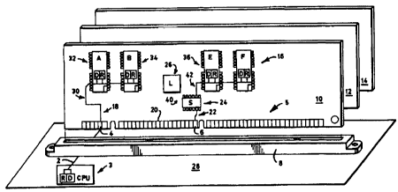
Figure 1 depicts a perspective view of the invention, showing the electronic
components on a multi-board memory configuration.
Figure 2a depicts a memory-timing diagram with no delay.
Figure 2b depicts a memory-timing diagram with a slight delay
Figure 2c depicts a memory-timing diagram with a large delay
nFTerr Fm r~FCrmpTrnN pF THE PREFERRED EMBODIMENTS
Referring now to Figure 1, the memory assembly consists of three boards, or
2o substrates 10, 12, 14. Substrate 10 contains an edge connector 5 which, in
turn,
contains a number of fingers which mate with connector 12, which is, in turn,
mounted on motherboard 28. The boards are substantially quadrangular, in
accordance with current standards for such boards. It will be seen that the
edge
connector is a comb-like array of individual conducting fingers. It should be
noted
CA 02334681 2000-12-08
WO 00!01207 PCT/US99/13836
7
that although three boards are included in this embodiment, there is no
inherent
limitation to the number of boards which may be included in the current
invention.
The boards shown may be mufti-layer boards, which are, in effect, a number of
connection layers bonded together. Interconnection between the different
layers, and
between the three substrates shown is by means of feed-throughs, plated-
through
holes which extend the width of each substrate, and which may connect with
conductive material on each layer. The chips shown mounted on the substrates
are
electrically connected through conductive mounting pads, which provide an
extended
conductive area to allow good contact between the pins of the computer chips
and the
leads on the substrates.
Although not shown in Figure l, it is often desirable, in order to present the
greatest density of computer chips possible, to mount these chips on both
mounting
surfaces of each substrate. It is clear that, regardless of how many layers of
conductive material are used in each substrate, only two mounting surfaces are
available.
Shown mounted on the motherboard 28 is a CPU 3, which is not part of this
invention. The signals conveyed to the memory board might be generated by a
controller chip rather than the CPU. In either case, the signals are connected
to the
memory board by means of a bus. At present, the computer bus consists of a
2o multiplicity of data lines, a multiplicity of separate address lines, and a
multiplicity of
control lines. When these lines are etched onto a printed circuit board, such
as the
motherboard or the memory board, they are called leads. In Figure l, a single
lead
only 2 is shown running from the CPU to the connector 5 via finger 4. The
single
lead is shown for the sake of clarity, although in reality there are a
multiplicity of such
CA 02334681 2000-12-08
WO 00/0120'7 PCT/US99/13836
8
leads. When the edge connector 5 is inserted into the connector 8, there will
be
electrical conductivity from finger 4 onto the memory board 10 via lead 30.
Still referring to Figure 1, a FET ( field-effect transistor) switch 24 is
mounted
on the memory board 10 and inserted in series with each DATA LINE. It should
be
noted that other types of switches are applicable to this application,
including, inter
alia, CMOS (Complementary Metal Oxide Semiconductor), and TTL (Transistor-
Transistor Logic) switches. Whatever technology is used, the switch should
have a
high impedance in the OFF, or disabled state, a low impedance and negligible
propagation delay in the ON, or enabled state, and low capacitance in both
states.
t o The switch must be bi-directional in the ON state with negligible
propagation delay in
both directions, and negligible transmission of the input signal in the OFF
state.
A single data lead 22 is shown for the sake of clarity, although in reality
there
are a multiplicity of such leads. The switch is placed as close to the edge
connector 5
as possible in order to minimize the distance of the lead 22 from the finger 6
to the pin
of the FET switch 24.
Also shown in Figure 1 are a number of DRAM chips A, B, E, and F. The
other corresponding pin of the switch is wired to the DRAM pins corresponding
to the
DATA LINE associated with DRAM chips E and F by means of lead 42, which is
electrically connected with lead 22 when the switch is closed, or in it ON
state. The
state of the switch is controlled by the logic decoder 26, which enables
switch 24 via
line 40. Again, there are a multiplicity of switches, driving the data leads
of the
memory chips via a multiplicity of leads; a unique enable line to the switch
could be
provided from the CPU or controller - however, a single lead 42 is shown for
the sake
of clarity.
CA 02334681 2000-12-08
WO 00/01207 PCT/US99/13836
9
When the switch is open, or in the OFF state, there will be a very high
impedance connection between the finger 6 and the lead 42. In effect, finger 6
appears to be the equivalent of an open circuit. The amount of capacitive load
presented to the DATA LINE of the BUS by the switch is less than 10 pF
(picofarads). The capacitive load presented by the DRAM chips and wires on the
side
of the FET switch facing the DRAMs is totally isolated from the data bus
lines.
When the switch is enabled, on the other hand, the DATA LINE sees the
additional capacitive load from the internal connection of the switch 24 to
the lead 42,
and its connections to the chips 36 and 16. If this internal load is 25 pF,
then the total
to load on the DATA LINE contributed by the selected memory chip is 30pF,
which
includes an additional SpF of stray capacitance.
Consider now, as an example, a typical memory system, containing 16
DIMMs, which has been tested using the current invention. If no DIMM is
selected,
the total capacitance seen by each data line is l OpF per DIMM, or a total of
160pF.
Assume next that a particular memory access selects only a single one of these
16 DIMMS. Then the capacitive load presented by the 15 DIMMs not selected will
be l OpF per DIMM, or 150 pF. In addition, the single selected DIMM will
contribute
30pF. Thus, the total capacitance presented to the bus will be 150pF plus
30pF, or
180pF.
2o Assuming that that the capacitance causes a delay of lone nanosecond (ns)
for
each SOpF, the delay resulting from this capacitance will be 3.6 ns.
In comparison, consider the system without the switch. The I 6 DIMMs will
present a capacitance of 16 times 30, or 480 pF. The resulting delay of 9.6ns
is about
three times as great, demonstrating the great improvement of the current
invention.
CA 02334681 2000-12-08
WO 00/01207 PCT/US99/13836
Using a figure of SOpF per lead rat~er that 25pF per lead, as is common in the
industry today, the figures are even more dramatic. Representing the stray
capacitance by the characters CL, the calculations show a capacitance of about
205pF
+CL with the use of the current invention, and about 800pF+CL using the
standard
method - a improvement of almost five to one. Experimental data using the
current
invention confirms these figures.
In an alternative embodiment, the signal (control signal) which controls the
FET switch is generated externally to the memory board, and conveyed to the
memory
board via the edge connector. This control signal may be generated on a
motherboard
1o to which the memory modules are mounted by a controller chip specifically
included
for this purpose. An alternate embodiment includes generation of this control
signal
on a central processing unit (CPU) or controller located on the motherboard.
In another alternative embodiment, the memory is an integral part of the
motherboard. As a result no separate memory boards or connectors therefor are
15 involved in the invention; instead, the FET switch is mounted on the
motherboard
itself between the memory chips and the bus, and performs the same function in
isolating the bus from the memory chips as in the first preferred embodiment.
In still another embodiment, the FET switches, or their equivalents, are
included within the memory chips themselves, which may be located on memory
2o boards, or directly on the motherboard itself. These FET switches are
controlled in
tum from the bus, which is connected to the memory modules.
In all of the alternative embodiments, the switches may be CMOS or TTL
switches, in addition to the FET switches previously described.
CA 02334681 2000-12-08
WO 00/01207 PCT/US99/13836
11
It will be apparent that improvements and modifications may be made within
the purview of the invention without departing from the scope of the invention
defined in the appended claims.