Note: Descriptions are shown in the official language in which they were submitted.
CA 02334684 2002-12-24
ELECTRO-LUMINESCENT DEVICE
The present invention relates to an elec:tro-
luminescent (EL) device, preferably used as a thin yet flat
form of display means.
An EL device comprising a light emitting layer formed
of an inorganic compound and inter=Leaned between upper and
lower insulator thin films is excellent in luminance
characteristics and stability upon driven on AC current.
EL devices fabricated through a fabrication process where
all process steps are carried out with thin-film
technologies are now used for a variety of displays. One
basic arrangement of such alight emitting device is shown
in Fig. 2.
This light emitting device has on a glass substrate 21
a multilayered film structure comprising a transparent
electrode 22 formed of Indium Tin Oxide (ITO) or the like,
a thin-film first insulator layer <?3 and a thin-film light
emitting layer 24 composed of an electroluminescence-
producing fluorescent material such as ZnS:Mn, and further
comprising on the light emitting layer 24 a thin-film
second insulator layer 25 and a bark electrode 26 formed of
an Al thin film or the like, and makes use of- light emitted
out of the transparent. glass substrate side.
Each of the thin-film first: and second insulator
layers is a transparent dielectric thin film made up of
Y203, Ta205, A1203, Si3N4, BaTi03, SrTi03, etc. , and formed by
a sputtering or evaporation prcacess.
These insulator layers perform important. functions in
limiting currents passing through t=he light emitting layer
to contribute to improvements in the stability of operation
and light emission of the thin-film EL device, and
protecting the light emitting layer against moisture and
CA 02334684 2000-12-07
-2-
harmful ion contamination to improve the reliability of the
thin-film EL device.
However, such a device has some practical problems.
One problem is that it is difficult to reduce the dielectric
breakdown of the device to nil over a wide area, resulting
in low yields, and another is that the applied driving
voltage necessary for the device to emit light becomes high
because voltage is dividedly applied to the insulator layers.
To solve the dielectric breakdown problem, it is
preferable to use an insulator material having good
dielectric strength properties. To provide a solution to
the light emission-driving voltage problem, it is preferable
to increase the capacity of the insulator layers, thereby
reducing the proportion of the voltage dividedly applied to
the insulator layers. In view of the principles of
operation of such a thin-film EL device of the AC driving
type, the current passing through the light emitting layer
contributing to light emission is virtually proportional to
the capacity of the insulator layers. To decrease the
driving voltage and enhance the luminance of Eight emission,
it is therefore of vital importance to increase the capacity
of the insulator layers.
For this reason, it is~attempted to use a ferroelectric
PbTi03 film of high dielectric constant formed by a
sputtering process as an insulator layer, thereby achieving
low-voltage driving. This PbTi03 sputtered film shows a
dielectric strength of 0.5 MV/cm at a relative permittivity
of 190 at most. However, the temperature of the substrate
must be elevated to about 600°C for PbTi03 film formation,
and so it is difficult to apply the PbTi03 film to the
fabrication of hitherto thin-film EL devices using a glass
substrate. Besides, a SrTi03 film formed by a sputtering
process, too, is known in the art. This SrTi03 sputtered
film has a relative permittivity of 140 and a dielectric
breakdown voltage of 1.5 to 2 Mv/cm. This .film is formed at
400°C. However, the practical use of the film for a thin-
film EL device using a glass substrate offers a problem
CA 02334684 2000-12-07
-3-
because an ITO transparent electrode is reduced and
blackened during film formation by sputtering.
One possible approach to solving this problem is to use
for the glass substrate a glass material that has a high
softening point and can be treated at high temperature. In
this case, however, the substrate costs much, and the upper
limit to the treatment temperature is again 600°C as well.
Another approach is to make insulator layers thinner.
However, the ITO film is susceptible to dielectric breakdown
at its edge because of the insufficient dielectric strength
of such thinner insulator layers. This is an obstacle to
development of large-area and large-capacity displays.
Thus, a conventional thin-film EL device must be driven
at high voltage, resulting in the need of using a costly
driving circuit of high dielectric strength. This
unavoidably makes displays costly and large-area displays
hardly achievable.
Among EL devices known to solve these problems, there
is an EL device wherein a thin-film light emitting layer 34,
a thin-film second insulator layer 35 and a transparent
second electrode 36 are stacked on a multilayered ceramic
structure comprising a ceramic substrate 31, a thick-film
first electrode 32 and a first insulator layer 33 of high
dielectric constant, as shown in Fig. 3.
In this EL device, a low-temperature sintering Pb
perovskite based material is used for the first insulator
layer. However, this material must be used with an
increased thickness because of its insufficient dielectric
strength. For this reason, it is impossible to reduce the
emission start voltage down to a sufficiently low level.
SUMMARY OF THE INVENTION
An object of the present invention is to use an
insulator layer, the dielectric strength of which is high
yet less susceptible to a change with time and the relative
permittivity of which is high yet less susceptible to a
change with time, thereby providing an EL device that is so
CA 02334684 2004-08-10
4
low in the emission-start voltage and emission-driving
voltage that stable light-emission performance can be
obtained.
In accordance with this invention an EL device has a
structure in which a first electrode formed according to a
predetermined pattern, a first insulator layer, an
electroluminescence-producing light-emitting layer, a
second insulator layer and a second electrode layer are
stacked successively on an electrical insulating substrate.
At least one of the first insulator layer and the second
insulator layer contains as a main component barium
titanate, and as subordinate components magnesium oxide,
manganese oxide, yttrium oxide, at least one oxide selected
from barium oxide and calcium oxide, and silicon oxide; the
ratios of magnesium oxide, manganese oxide, yttrium oxide,
barium oxide, calcium oxide and silicon oxide, with respect
to 100 moles of barium titanate, being:
MgO: 0.1 to 3 moles,
MnO: 0.05 to 1.0 mole,
Y203: 1 mole or less,
Ba0 + CaO: 2 to 12 moles, and
Si02: 2 to 12 moles,
as calculated on MgO, MnO, Y203, BaO, CaO, Si02 and BaTi03
bases, respectively. The first insulator layer has a
thickness of 10 um or less.
Preferably, 'the electrical insulating substrate and
the first insulator layer each are formed of a ceramic
material.
Also preferably, the EL device contains BaO, Ca0 and
Si02 in a form represented by (BaXCal-XO) y~SiOz, where 0. 3 <- x
0.7 and 0.95 < y < 1.05, and in an amount of 1% to 10~ by
weight with respect to the sum of BaTi03, MgO, Mn0 and Y203.
In a preferred embodiment the first electrode of the
EL device is formed of at least one metal
CA 02334684 2000-12-07
-5-
selected from Ni, Cu, W and Mo or an alloy composed mainly
of at least one metal selected from said metals.
BRIEF EXPLANATION OF THE DRAWINGS
Fig. 1 is a sectional view in schematic from depicting
the EL device according to the present invention.
Fig. 2 is a sectional view in schematic form depicting
a conventional thin-film EL device.
Fig. 3 is a sectional view in schematic form depicting
a conventional EL device using a mutilayered ceramic
structure.
DETAILED EXPLANATION OF THE PREFERRED EMBODIMENTS
Some illustrative embodiments of the present invention
will be explained in detail.
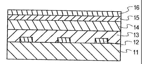
One basic arrangement of the EL device according to the
present invention is shown in Fig. 1. The EL device of the
present invention has a structure comprising an electrical
insulating substrate 11, a first electrode 12 formed
according to a predetermined pattern and a first insulator
layer 13, and is provided thereon with a basic structure
comprising an electroluminescence-producing light emitting
layer 14 formed by a vacuum evaporation process, a
sputtering process, a CVD process or the like, a second
insulator layer 15 and a second electrode layer 16 formed
preferably of a transparent electrode. At least one of the
first insulator layer 13 and the second insulator 15 is
formed of such a specific composition as detailed below.
The light emitting layer 14 is similar to that used in
an ordinary EL device, and the second electrode 16 is an ITO
or other film formed using an ordinary thin-film process.
For preferable materials for the light emitting layer,
for instance, use may be made of such materials as described
in Shosaku 'Tanaka, "Technical Trends in Recent Displays",
Monthly Display, pp. 1-10, April 1998. More specifically,
ZnS, Mn/CdSSe, etc. are used as the material to obtain red
light emission, ZnS:TbOF, ZnS:Tb, ZnS:Tb, etc. are used as
the material to obtain green light emission, and SrS:Ce,
CA 02334684 2000-12-07
-6-
(SrS:Ce/ZnS)n, CaGa2S4:Ce, Sr2Ga2S4:Ce, etc. are used for the
material to obtain blue light emission.
SrS:Ce/ZnS:Mn, etc. are known for the material to
obtain white light emission.
Especially, the most preferable results can be obtained
when the present invention is applied to an EL device
comprising a blue light emitting layer of SrS:Ce studied in
IDW (International Display Workshop), '97 X. Wu.,
"Multicolor Thin-Film Ceramic Hybrid EL Displays", pp. 593-
596.
No particular limitation is imposed on the thickness of
the light emitting layer; however, it is understood that too
thick a light emitting layer leads to a driving voltage
increase whereas too thin a light emitting layer causes an
emission efficiency drop. For instance, the light emitting
layer has a thickness of the order of preferably 100 to
1,000 nm, and more preferably 150 to 500 nm, a:lthough
varying depending on the fluorescent material used.
The light emitting layer may be formed by vapor-phase
deposition processes represented by physical vapor-phase
deposition processes including a sputtering or evaporation
process, and chemical vapor-phase deposition processes such
as a CVD process, among which the chemical vapor-phase
deposition processes such as a CVD process are preferable.
As described in the aforesaid IDW in particular, a
light emitting layer of SrS:Ce, when formed by an electron
beam evaporation process in a H2S atmosphere, can have an
ever-higher purity.
It is preferable to carry out thermal treatment after
the formation of the 1_ight emitting layer. The thermal
treatment may be carried out after the electrode layer,
insulating layer and light emitting layer are stacked on the
substrate in this order or cap annealing may be carried out
after the electrode layer, insulating layer, light emitting
layer and insulating layer optionally with an electrode
layer provided thereon are stacked on the substrate in this
order. Usually, it is preferable to use a cap annealing
CA 02334684 2000-12-07
_7-
process. The heat treatment temperature used herein should
be preferably between 600°C and the substrate sintering
temperature, more preferably between 600°C and 1,300°C, and
even more preferably between about 800°C and about 1,200°C,
and the heat treatment time used herein should be between 10
minutes and 600 minutes, and especially between about 30
minutes and about 180 minutes. The annealing atmosphere
used herein should preferably be N2, Ar, He, or N2 with up
to 0.1~ of 02 contained therein.
For the transparent electrode material, it is
preferable to use a material of relatively low resistance
because of the need of generating an electric field with
high efficiency. For instance, it is preferable to use a
material composed mainly of any one of tin-doped indium
oxide (ITO), zinc-doped indium oxide (IZO), indium oxide
(In203), tin oxide (Sn02) and zinc oxide (Zn0). These
oxides may deviate slightly from their stoichiometric
compositions. The mixing ratio of Sn02 with respect to
In203 should be between 1 wto and 20 wt~, and preferably
between 5 wt~ and 12 wt%. In IZO, the mixing ratio of Zn0
with respect to In203 should usually be of the order of 12
wt~ to 32 wt~.
When the ferroelectric material having the specific
composition detailed below is used for the first insulator
layer, it is preferable that the substrate, first electrode
and first insulator layer form together a multilayered
ceramic structure. In this case, the first insulator layer
and substrate may be made up of the same material or the
same material system.
The first insulator layer comprises a barium titanate
based ferroelectric material containing as a main component
barium titanate and as subordinate components magnesium
oxide, manganese oxide, at least one oxide selected from
barium oxide and calcium oxide, and silicon oxide. In the
insulator layer, the ratios of magnesium oxide, manganese
oxide, barium oxide, calcium oxide and silicon oxide with
respect to 100 moles of barium titanate are:
CA 02334684 2000-12-07
_g_
MgO: 0.1 to 3 moles, and preferably 0.5 to 1.5 moles,
MnO: 0.05 to 1.0 mole, and preferably 0.2 to 0.4 moles,
Ba0+CaO: 2 to 12 moles, and
Si02: 2 to 12 moles
as calculated on MgO, MnO, BaO, CaO, Si02 and BaTi03 bases,
respectively.
Usually, ;_t is preferable that (Ba0+Ca0)/Si02 is in the
range of 0.9 to 1.1 although there is no particular limit
thereto. BaO, Ca0 and Si02 may be contained in the form of
(BaXCa1_XO)y~Si02. To obtain a closely packed sintered body,
it is then preferable that 0.3 <_ x <_ 0.7 and 0.95 __<y <_ 1.05.
The content of (BaXCa1_XO)y~SiO~ should be preferably
between 1 wt% and 10 wt%, and more preferably between 4 wt%
and 6 wt% with respect to the sum of BaTi03, Mg0 and MnO.
It is noted that no particular limitation is imposed on
the oxidized state of each oxide; the content of the metal
element forming each oxide should be within the above range.
The first insulator layer should preferably contain as
an additional subordinate oxide yttrium in an amount of up 1
mole, as calculated on a Y203 basis, with respect to 100
moles of barium titanate as calculated on a BaTi03 basis.
There is no particular lower limit to the content of Y203;
however, it is preferable that the content of Y203 should be
0.1 mole or greater to make full use of its effect. When
yttrium oxide is used, the content of (BaXCal_x0)y~Si02
should be preferably between 1 wt% and 10 wt%, and more
preferably between 4 wt% and 6 wt% with respect to the sum
of BaTi03, MgO, Mn0 and Y203.
It is acceptable that the first insulator layer
contains other compound; however, it is preferable that the
first insulator layer should be substantially free from
cobalt oxide because it gives rise to a large capacity
change.
The contents of the subordinate components should be
limited to the above ranges for the following .reasons.
When the content of magnesium oxide is below the lower
limit of the above range, the temperature property of
CA 02334684 2000-12-07
-9-
capacity deteriorates. When the content of magnesium oxide
exceeds the upper limit of the above range, sinterability
drops sharply and so close-packing becomes insufficient,
resulting in an increase in the change of dielectric
strength with time. This in turn makes it difficult to use
the first insulator layer in a thin-film form.
When the content of manganese oxide is below the lower
limit of the above range, no satisfactory reduction
resistance is obtained. When easily oxidizable Ni is used
1.0 for the first electrode, it is difficult to use the first
insulator layer in a thin-film form due to a 7_arge change of
dielectric strength with time. When the content of
manganese oxide exceeds the upper limit of the above range,
the change of capacity with time becomes larger and so the
change-with-time of emission luminance of the light emitting
device becomes larger.
When the contents of Ba0+CaO, Si02 and (BaXCa1_XO)y~Si02
are too small, the change of capacity with time becomes
large and so the change of emission luminance with time
becomes large. Too much causes the dielectric constant to
drop sharply, resulting in a rise of the emission start
voltage and a luminance drop as well.
Yttrium oxide improves on the durability of dielectric
strength. When the content of yttrium oxide exceeds the
upper limit of the above range, the capacity decreases,
sufficient close-packing is often unachievable due to a
sinterability drop.
The first insulator layer may contain aluminum oxide.
By the addition of aluminum oxide, it is possible to lower
the sintering temperature. The content of aluminum oxide as
calculated on an A1203 basis should preferably account for 1
wt~ or less of the first insulator layer material. Too much
aluminum oxide rather hinders the sintering of the first
insulator layer.
No particular limitation is placed on the average
crystal grain diameter of the first insulator layer. By
allowing the first insulator layer to have the above
CA 02334684 2002-12-24
composition, it can be obtained in a fine crystal form.
Usually, the average crystal grain diameter is of the order
of 0.2 to 0.7 Vim.
Although the conductive material for the first
5 electrode layer used with the aforsaid multilayered ceramic
structure is not critical, yet materials containing one or
two or more of Ag, Au, Pd, Pt, Cu, Ni, W, Mo, Fe and Co or
any one of Ag-Pd, Ni-Mn, Ni-Cr, Ni-Co and Ni-A1 alloys
should preferably be used.
10 When firing is carried out in a reducing atmosphere,
base metals may be selected from these materials.
Preference is given to one or two or more of Mn, Fe, Co, Ni,
Cu, Si, W, Mo, etc. or any one of Ni-Cu, Ni-Mn, Ni-Cr, Ni-Co
and Ni-Al alloys, among which Ni and Cu as well as Ni-Cu,
alloys, etc. are most preferred.
When firing is carried out in an oxidizing atmosphere,
metals that are not converted to oxides in the oxidizing
atmosphere should preferably be used. To be more specific,
one or two or more of Ag, Au, Ft, Rh, Ru, Ir and Pd may
be used, although Ag and Pd as well as Ag-Pd alloys are
particularly preferred.
When the above multilayered ceramic structure is used,
no particular limitation is again placed on the material for
the substrate. However, it is preferable to use A1203
optionally with Si02, MgO, CaO, etc. added thereto for
various purposes, for example, for sintering temperature
control. When such a multilayered ceramic structure is not
used, use may be made of a glass substrate employed for an
ordinary EL device. However, ir_ is preferable to use a
high-melting point glass that can be treated at higher
temperatures.
The above multilayered structure may be fabricated by
an ordinary fabrication process. More specifically, a
binder is mixed with the starting ceramic powders that are
to provide a substrate, thereby making a paste. Then, the
paste is formed into film by casting to make a green sheet.
The first electrode Ito provide a ceramic internal electrode
CA 02334684 2000-12-07
-11-
is printed on the green sheet by a screen printing process
or the like.
Then, the assembly is fired, if required, after which a
paste prepared by mixing a binder with high dielectric
material powders is printed on the assembly by a screen
printing process or the like. Finally, firing yields a
multilayered ceramic structure.
Firing following binder removal is carried out at 1,200
to 1,400°C, preferably 1,250 to 1,300°C for several tens of
minutes to a few hours.
For firing, the oxygen partial pressure should
preferably be between 10-g atm. and 10-12 atm. Since the
first insulator layer is placed in a reducing atmosphere
under this condition, any one metal selected from
inexpensive base metals such as Ni, Cu, W and Mo or an alloy
composed mainly of one or more such metals may be used for
the electrode. If required in this case, the green sheet
and first electrode pattern may be fired while a layer for
preventing diffusion of oxygen, e.g., the same layer as the
first insulator layer is located between them.
When firing is carried out in the reducing atmosphere,
it is preferable to anneal the composite substrate.
Annealing is the treatment for re-oxidizing the first
insulator layer, so that the change of dielectric strength
with time can be reduced.
The partial pressure of oxygen in the annealing
atmosphere should preferably be 10-6 atm. or greater, and
especially between 10-5 atm. and 10-~ atm. When the oxygen
partial pressure is below the lower limit of the above range,
it is difficult to re-oxidize the insulator layer or the
dielectric layer. At an oxygen partial pressure exceeding
the upper limit of the range, the internal conductor tends
to oxidize.
The holding temperature for annealing should preferably
be 1,100°C or lower, and especially between 500°C and
1,000°C. When the holding temperature is below the lower
limit of the above range, the oxidization of the insulator
CA 02334684 2000-12-07
-12 ~-
layer or the dielectric layer tends to become insufficient,
resulting in life reductions. At a holding temperature
exceeding the upper limit of the range, the electrode layer
tends to oxidize, not only resulting in a capacity drop but
also leading to reactions with the insulator material or the
dielectric material, which again give rise to life
reductions.
It is noted that the annealing step may be built up
only of either a heating cycle or a cooling cycle. In this
case, the temperature holding time is zero; in other words,
the holding temperature is tantamount to the highest
temperature. The temperature holding time should preferably
be between 0 hour and 20 hours, and especially between 2
hours and 10 hours. For the atmospheric gas, it is
preferable to use a wetted N2 gas, etc.
Many other fabrication processes may be applied to the
multilayered ceramic structure.
For instance, the following two processes may be used.
(1) One process comprises the steps of providing a film
sheet such as a PET film sheet, printing a paste containing
a given dielectric material for the first insulator layer
all over the surface of the film sheet using a printing
process or the like, forming a paste pattern containing an
electrically conductive material for the first electrode on
the first paste using a screen printing process or the like,
forming a green sheet formed of a paste containing alumina
and other additives for the substrate on the second paste to
prepare a multilayered structure, and sintering the
structure from which the film sheet is removed. In this
case, a light emitting layer and so on are formed on the
surface of the structure that was in contact with the film
sheet. This process is characterized in that a very flat
surface is obtainable.
(2) Another process comprises the steps of providing a
previously fired alumina or other ceramic substrate, forming
a paste pattern containing an electrically conductive
material for the first electrode on the surface of the
CA 02334684 2004-08-10
-13-
substrate, printing a paste containing a given dielectric
material for the first insulator layer all over the surface
of the first paste using a screen printing process or the
like, and sintering the assembly including the substrate.
An EL device emits light at portions defined by the
first and second electrodes that intersect at right angles,
so that images can be displayed thereon. The electrodes
have a combined current supply and pixel display function,
and are formed according to any desired pattern if required.
When the substrate, first electrode and first insulator
layer are fabricated in the form of a multilayered ceramic
structure, the pattern for the first electrode may be easily
formed by a screen printing process. For ordinary EL device
displays, it is hardly required to form extremely fine
electrode patterns; the screen printing process that enables
an electrode to be formed over a large area at low costs can
be used. When a fine electrode pattern is demanded,
photolithography may be used.
As explained above, the ceramic material having a
specific composition is used for at least one of the first
and second insulator layers that are the important elements
that form an AC type EL device according to the present
invention. This ceramic material is preferable as the
insulator layer in the EL device because of having a
relative permittivity of 2,000 or greater and a dielectric
strength of 150 MV/m.
For an EL device using a conventional ceramic structure,
the first insulator layer must have a thickness of 30 to 40
~m in order to prevent a breakdown of the first insulator
layer. According to the present invention, however, the
thickness of the first insulator layer is reduced down
to 10 ~m or less, and especially 2 to 5 Vim, so that the
emission driving voltage of the EL device can be lowered.
This means that when a device is used with the same emission
luminance, that device can be driven at a lower driving
voltage. This is very effective for driving circuit design.
CA 02334684 2000-12-07
-14-
The first insulator layer according to the present
invention has an increased breakdown voltage and is improved
in terms of the change of relative permittivity with time at
a constant applied voltage, and so ensures stable light
emission over an extended period of time.
The light emitting layer, etc. are formed on the
multilayered ceramic structure explained above by a thin-
film process such as evaporation or sputtering, thereby
obtaining an EL device according to the present invention.
EXAMPLE
A binder was mixed with a mixture of A1203 powders with
Si02, Mg0 and Ca0 powdery additives to prepare a paste,
which was then cast into a green sheet forming a ceramic
substrate of 1 mm in thickness. Using a screen printing
process, a Ni paste was formed on this ceramic precursor
according to a striped pattern of 0.3 mm in width, 0.5 mm in
pitch and 1 ~m in thickness. For the material for the first
insulator layer, a paste containing pre-fired powders having
the composition shown in Table 1 was prepared, This paste
was then printed all over the surface of the green sheet
with the electrode pattern formed thereon. The post-firing
thickness of the printed paste was 4 ~Lm.
CA 02334684 2000-12-07
-15-
a~
N
'4'r
d
. O 00 o t~ ov t~ t~ t~ c cd
,~ ~
~
O
N M N N N N 00
N
N r~
.rr
V ~ r r d~ +~
~
~r ~r ~ ~ ~ .
~'' ~ f-I O
r-I
"
O
3
U
O
p
rd p
~
~
x O o 0 0 0 0 0 ~o o
O G~.~,-i,~ ,~ ,--i~ ~ - o
"
N o
a
0 0 0 0 0 0 o p O
M N C1 d' I~ 00 x tn
w op m ow c o o M U cd
N N N N M M M .,.~ +.r
+~ O
td d' I~ 00 h O~ td
"'
O
'~ O N r-I N O
~
~
'~"' O O O O O O O td 'rl
~
.1~ rl
'
cd b f3~
f3'
-i U p ~ c
d
~ ~
~.1 b
~
b U V W w n m m n ~ U
H O 3 ri +~
b
o i ~ u n ~n
M r1 M M M
O O td
4-I
~ 0 0 0 0 0 , ~
0
3
3
b
m -- b ~d
o ~ x
c
d
W 0
p
U
f
-I
rl ,Ll
N 3
.~ o
O N rd ~d
r'I ri N
.
~ ~ H b
z ,
0
U
.J
rl N M ~N tn vD l''
CA 02334684 2000-12-07
-16-
The binder was removed from the green sheet under given
conditions. Following this, the green sheet was held at
1,250°C for a constant time in a mixed gas atmosphere
composed of wetted N2 and H2 (having an oxygen partial
pressure of 10-9 atm.) for firing, and then subjected to the
above oxidization, thereby preparing a multilayered ceramic
structure.
Then, ZnS:Mn was vacuum evaporated on the ceramic
structure to a thickness of 0.3 ~m by co-evaporation of ZnS
and Mn. For property improvements, the ceramic structure
was annealed in Ar at 650 to 750'C for 2 hours. Afterwards,
a 0.3 ~m thick TaA109 insulator layer was formed by a
sputtering process using a target consisting of a mixture of
Ta205 and A1203 to form the second insulator layer. Then, a
0.4 ~m thick ITO film was formed by a sputtering process.
Subsequently, the ITO film was etched at 0.3 mm width and
0.5 mm pitch while it was arranged at right angles with the
aforesaid Ni thick-film, striped electrode, thereby
preparing a transparent striped electrode.
The emission start voltage of the obtained EL device
samples and the relative permittivity and breakdown voltage
of the separately prepared first insulator layer samples are
shown in Table 1. The properties of one comparative sample
obtained using a BaTi03 thick film with no additives (MnO,
etc.) added thereto are also indicated. In this case, the
first insulator layer was formed with a thickness of 100 ~m
because its breakdown voltage was low.
When the BaTi03 based ferroelectric film having such a
specific composition as used herein is used for the first or
second insulator layer in a conventional thin-film type EL
device, use may be made of co-evaporation using molecular
beam epitaxy, ion-assisted ion beam sputtering or the like.
In this case, too, the same effects as those of an EL device
using the aforesaid multilayered ceramic structure are
obtained by use of a heat-resistant substrate.
EFFECT OF THE INVENTION
CA 02334684 2000-12-07
-17-
According to the present invention as explained above,
the BaTi03 based dielectric material having a specific
composition is used for the first insulator layer in the
multilayered ceramic structure comprising the substrate,
first electrode layer and first insulator layer, so that an
EL device can be obtained, which can be driven at a low
driving voltage, and is less susceptible to a dielectric
breakdown even when high voltage is applied thereon, thereby
ensuring stable light emission performance over an extended
period of time.
The composite substrate, because of having been fired
at high temperature, allows the light emitting layer to be
thermally treated at a hs.gh temperature lower than the
firing temperature, so that light emission performance is
stabilized with enhanced luminance.