Note: Descriptions are shown in the official language in which they were submitted.
CA 02335124 2000-12-14
VlrO 99/65144 PCT/NZ99/00082
1
GATE DRIVE FOR INSULATED GATE POWER SEMICONDUCTORS
Technical Field
The present invention relates to an analogue gate drive for insulated gate
power
semiconductors. More specifically it relates to control of the current and
voltage switching
trajectories of insulated gate power semiconductor switches, which has
application in the
area of fundamental power electronics.
Back4round Art
MOSFETs and insulated gate bipolar transistor devices (IGBTs) are used in
switch mode
power supplies (SMPS) because of their easy driving ability and their ability
to handle high
currents and voltages at high-switching frequencies.
However, the switching trajectories for both types of devices are responsible
for both
common-mode electromagnetic emissions generated by the drain current waveform
and
power losses in the commutation cell. These two characteristics represent
opposing design
objectives for power converters. As requirements of miniaturisation drive the
switching
frequencies higher, a satisfactory trade off between electromagnetic
interference (EMI) and
power losses becomes increasingly difficult.
The characteristic rectangular voltage waveform of SMPS is modelled as a
periodic
trapezoidal pulse train. This waveform produces E-field radiation and common
mode
conducted interference which is caused by parasitic capacitances to ground
returns.
CA 02335124 2000-12-14
WO 99/65144 PCT/NZ99/00082
2
Electrostatic screening (of known type) and circuit references (Zverev et al,
Proc. IEEE PESC
'97, Missouri, USA) can be used to minimise the effects of electromagnetic
field and any
induced common mode coupling. However the similarity of the rectangular
switching
currents in the commutation circuitry produces significant changing magnetic
flux. This
induces high frequency noise throughout the circuit, resulting in H-field
radiation and
interference with harmonics, which can extend beyond 100Mhz.
An additional constraint on any design or modification is that the device must
still be
electromagnetically compatible (EMC) (that is, complying with all applicable
standards, for
example the European CISPR recommendations).
Also, in the avoidance of the problems associated with EMC, magnetic material
for shielding,
such as steel, can be used. However the performance of such shields drops off
sharply
above 500KHz.
Improvement methods for power converters that are EMC fall into three classes.
Firstly,
there are methods of containment and dissipation, such as shielding. Secondly,
parasitic
components contributing to EMI can be minimised. An example of such a method
is to
minimise the current loop area through decoupling and layout.
Thirdly are methods that allow for the reduction of EMI generated at the
commutation source.
Such methods can be effective but can add significant complexity to the design
of any
device. For example, soft switching resonant and quasi-resonant topologies can
be used.
CA 02335124 2000-12-14
WO 99/65144 PCT/NZ99/00082
3
However, the drawback of such a method is the higher conduction loss, higher
voltage stress
and more numerous or larger componentry.
A further example of these third methods is one that slows the current rise
and fall times with
the addition of gate resistors. However the disadvantage is that the gate
resistor limits the
amount of current available to charge the parasitic gate-drain capacitance
(Miller capacitance)
as the drain voltage changes. This leads to slow voltage switching times.
However the trade off between EMI and power loss is becoming increasingly
difficult as
switching frequencies move higher.
An alternative approach is to eliminate or reduce EMI generation at its
source. One possible
solution is that disclosed by Consoli et al ("An innovative EMI reduction
design technique in
Power Converters", IEEE Trans. On Electromagnetic Compatibility, Vol 38, No.
4, Nov. 96)
and by Musumeci et al ("Switching-behaviour Improvement of Insulated Gate-
Controlled
Devices", IEEE Trans. On power electronics, Vol. 12, No. 4, July 19971. The
solution
proposed by both is an EMI reduction technique based on a digital method,
using carefully
timed current sources to overcome the miller capacitance effect during
switching.
An object of the present invention is the provision of an analogue gate drive
technique which
allows the independent and optimal control of the drain current and voltage
waveforms in
switched mode converters using insulated gate power devices.
CA 02335124 2000-12-14
VI~O 99/65144 PCT/NZ99/00082
4
A further object of the present invention is the provision of a gate drive
technique which
overcomes or at least mitigates some of the abovementioned disadvantages, or
at
least provides the public with a useful choice.
Disclosure of Invention
According to a first aspect of the invention there is provided a circuit for
independent control
of drain current and voltage for an insulated gate switching circuit, for a
switching mode
power supply, said circuit including:
an insulated gate semi-conductor device;
a linear buffer; and
a combined voltage source and current source within a local feedback loop
operable
during turn-off; wherein the rate of change of current is controlled by the
gate voltage
traversing the transconductance curve.
According to a second aspect of the invention there is provided a gate drive
circuit for an
insulated gate semiconductor device including:
a voltage source;
a current source; and
a feedback signal, wherein a combination of the voltage source and current
source are
adapted to provide a gate signal for an insulated gate semiconductor device,
such that
the gate signal allows independent control of drain current and drain voltage
during the
turn-on or turn-off of said insulated gate semiconductor.
CA 02335124 2000-12-14
WO 99/65144 PCT/NZ99/00082
Preferably the feedback signal is the gate charge (or discharge) current of an
insulated gate
semiconductor.
Preferably the voltage and current components of the gate signal are adapted
to be co-
5 dependant depending on the feedback signal.
Preferably the gate signal output is a linear buffer having a low impedance
output and in
particular the linear buffer is an operational amplifier of similar.
Preferably the voltage source and current source may be a combined voltage and
current
source having a low output impedance.
Preferably the voltage source and current source are adapted to provide either
current control
or voltage control of the driving signal depending upon the state of the
feedback signal.
Preferably the rate of change of drain current is controlled by the voltage
source traversing a
transconductance curve of an insulated gate semiconductor.
Preferably the rate of change of the drain voltage is controlled by dynamic
variations in the
current source due to feedback.
Preferably the gate signal is the gate signal of either a MOSFET or an IGBT.
CA 02335124 2000-12-14
WO 99/65144 PCT/NZ99/00082
6
According to another aspect of the present invention there is provided a
circuit for
independent control of drain current and voltage for an insulated gate
switching circuit, for a
switching mode power supply, said circuit including:
a low impedance controlled ramp voltage source, to control the drain voltage
slope and
drain current slope during switching;
a low impedance voltage linear buffer with a ramp function as its input;
wherein both
the voltage source and the linear buffer are operable during turn-on, wherein
the rate
of change of the voltage is limited by the output impedance of the buffer.
Preferably the rate of change of drain current is controlled by the voltage
source traversing a
transconductance curve of an insulated gate semiconductor.
Preferably the gate signal is the gate signal of either a MOSFET or an IGBT.
Brief Description of Drawincts
By way of example only, a preferred embodiment of the present invention is
described in
detail with reference to the accompanying drawings, in which :-
Figiure 1: is a circuit diagram including a known MOSFET gate drive circuit;
Figure 2: is a graph showing the waveforms of the circuit of Figure 1;
Figure 3: is a diagrammatic representation of a first preferred embodiment of
a
turn-on circuit of the present invention;
Figure 4: is a diagrammatic representation of a first preferred embodiment of
a
turn-off circuit;
CA 02335124 2000-12-14
WO 99/65144 PCT/NZ99/00082
7
Figure 5a: is a graphic representation of the drain voltage, gate voltage and
drain
current waveforms for known gate drives;
Figure 5b: is a graphic representation of the drain voltage, gate voltage and
drain
current waveforms for the circuits of the present invention during turn-
on;
Figure 6: is a graphic representation of the near-field radiated emission
measurements of the prior art and that resulting from the turn-on circuits
of the present invention;
Figure 7: is a circuit diagram of a full gate drive circuit for both the turn-
on and
turn-off phases of a semiconductor switching cycle; and
Figure 8: is a block diagram of the microprocessor control of the gate drive
circuit
shown in Figure 7.
Best Mode for Carryina Out the Invention
It is useful to review the switching characteristics for insulated gate
devices and the effect of
the traditional gate resistance. The more general case for the MOSFET will be
used. Referring
to Figure 1, a conventional MOSFET gate drive circuit 2 is thereshown.
Parasitic
capacitances Cgd and Cgs are shown for illustrative purposes only and are not
circuit
components. The circuit includes a high performance digital buffer with a
series gate resistor
Rg to control the drain current rise and fall times.
Figure 2 shows the oscilloscope waveforms from the circuit of Figure 1. The
switching
frequency used is 100KHz, with voltage waveforms of 5V/div and current
waveforms of
1 ~4/div. Initially the gate-source voltage Vgs rises exponentially until it
reaches the threshold
CA 02335124 2000-12-14
WO 99/65144 PCT/NZ99/00082
8
voltage and the device starts turning on. The drain current Id begins to rise
following the
MOSFET transconductance curve. The drain-source voltage Vds remains clamped at
its initial
value Vo as long as the drain current Id is less than full load current to and
free wheeling
diode Df is conducting.
Once the MOSFET is carrying the full load current lo, but is still in the
active region, the gate-
source voltage Vgs remains constant even thought the gate circuit may be
supplying current
to the gate. This is due to the drain voltage Vds beginning to decrease
requiring discharge of
the gate-drain capacitance Cdg through Rg thereby limiting the rate of change
of the drain
voltage (dVdg/dt). This is known as the miller effect, and the region between
A and B on
Figure 2 represents the Miller effect zone. The decrease in drain voltage Vds
is non-linear and
is caused by dynamic variation of the gate-drain capacitance Cgd as the drain-
source voltage
Vds changes. Thus Rg limits both dla/dt and dVes/dt thereby requiring a trade-
off between
reduced EMI and power loss. Once the miller effect ends, the gate voltage Vgs
can continue
to increase to its final value. As can be seen from Figure 2 the above is also
the case during
the turn-off phase, except that current is being extracted from the gate
capacitance and the
order of current and voltage are reversed.
Referring to Figure 3 a schematic of the circuit of a first preferred
embodiment is thereshown.
A digital input signal controls two current sources which make a ramp signal
appear at the
input to the linear buffer. Variable resistors VR1 and VR2 control the rise
and fall times
respectively. The linear buffer U1 is a high speed bipolar buffer of known
type. An example
of such a buffer is the buffer EL2009C (of Elantec Incl.
CA 02335124 2000-12-14
WO 99/65144 PCTlNZ99/00082
9
During switching, the standard gate resistor Rg (shown in Figure 1 ), combined
with gate
source capacitance Cgs, causes a voltage ramp at the MOSFET gate, which
controls the drain
current Id rate of change. In the standard circuit of Figure 1, gate resister
Rg also limits the
current available to charge and discharge the MOSFET gate-drain capacitance
Cgd. In the
embodiment shown in Figure 3, control of both the drain current Id slope and
drain voltage
Vds slope (shown in Figure 2) are optimised using a low impedance voltage
source, making it
is possible to remove the gate resistor Rg altogether. This low impedance
voltage source can
be achieved with the use of a low impedance linear buffer U 1 with a ramp
function as its
input. In this way, the di/dt slope is controlled by the gate voltage Vgs
traversing the
MOSFET transconductance curve, and dv/dt is limited only by the output
impedance of the
buffer U1, minimising both H-field emissions and power loss. Using this method
the Miller
zone in the gate switching trajectory of Figure 2 is all but eliminated.
Unfortunately this simple circuit has a problem during turn-off, resulting in
insufficient control
of the drain di/dt (off). A more complex hybrid source involving feedback of
the gate current
overcomes this problem, and introduces the additional ability to directly
control the drain
voltage Vds rise and fall times (rather than automatically as fast as the
output impedance of
the buffer will allow).
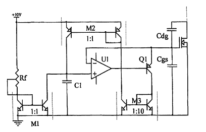
Referring to Figure 4 a preferred embodiment of the turn-off portion of a gate
drive circuit
utilising feedback of gate current, as described above, is thereshown. This
includes a
combination voltage source and current source within a local feedback loop.
The operation of
this circuit will now be explained, but for simplicity, only the case for turn-
off only will be
described. For the MOSFET this description is the direct inverse of the turn-
on phase. For the
CA 02335124 2000-12-14
Vi~O 99/65144 PCT/NZ99/00082
purpose of this explanation we will assume that C1 - Cgs and that the nominal
Cgs
discharge current is 0.1 A.
Rf sets the discharge current for capacitor C1, which is initially charged to
the normal on
5 state gate voltage Vgslon). This creates a voltage ramp on capacitor C1 and
gate-source
capacitance Cgs due to the operation of the unity gain buffer U1 in
conjunction with the
emitter follower Q1. Buffer U1 eliminates the base-emitter voltage drop that
would normally
occur across emitter-follower Q1. This has significance during the current
rise-time interval
described shortly. Emitter-follower Q1 provides current gain isolating
capacitor C1 from gate
10 source capacitance Cgs. During this time current mirror M3, which has a
10:1 reduction
characteristic, injects 0.01 amps into capacitor C1 through current mirror M2.
This negative
feedback results in stabilisation of the current discharge to just under 0.1
amp.
When the voltage ramp reaches on state gate voltage, the drain voltage will
start to rise,
requiring the gate voltage to plateau as the discharged current is diverted to
drain gate
capacitance Cdg. This voltage plateau results from the operation of current
mirrors M3 and
M2. The drain gate capacitance Cdg discharge current through emitter follower
Q1 quickly
increases until it reaches 1 amp at which time current mirrors M3 and M2 will
be injecting
0.1 amps into capacitor C1.
As this injected current is equal to the discharge current set by current
mirror M 1, the voltage
on capacitor C1 will be static, thereby allowing a voltage plateau.
CA 02335124 2000-12-14
WO 99/65144 PCT/NZ99/00082
11
Buffer U1 provides internal gain to eliminate the slight increase in base
emitter voltage
required to increase the collector current in emitter follower Q1 from 0.1
amps to 1.Oamp. At
the end of the Miller region drain gate capacitance Cdg is fully charged and
the discharged
current is transferred back to gate source capacitance Cgs, resuming the ramp
on the gate
source voltage. The discharge current drops back to 0.1 amp virtually
instantaneously as
attempts to discharge the gate source capacitor Cgs faster than capacitor C1
turns off
emitter follower Q1.
The circuit is thus self-regulating and the gate voltage is controlled in the
pre-determined
manner. Consequently the drain current falls at the programmed rate. The
current ratio at
current mirror M3 can be set to a pre-determined (high) value for the
described improvements
in the voltage rise-time during turn-off, without affecting the drain current
slope.
As described, earlier the embodiment shown in Figure 4 is only the turn-off
portion of the
circuit. Obviously for practical implementation the improved gate drive
preferably exhibits
improvements to both turn-on and turn-off the semiconductor switch. An
embodiment of the
invention which provides a improvement to both the turn-on and turn-off
portions of the
switching cycle is shown in Figure 7. This circuit has the same operation of
that shown in
Figure 4, except with the inclusion of mirror componentry for operation in the
turn-on phase
of the switching cycle. Current mirrors M2 and M5 have been added to provide
for the gate
current inversion which occurs between the turn-on and turn-off phases.
Parasitic
capacitances Cdg and Cgs are not shown in Figure 7.
CA 02335124 2000-12-14
WO 99/65144 PCT/NZ99/00082
12
The representations shown in Figure 7 of the invention provide a mechanism to
independently
and continuously control the slope of both the drain voltage and drain current
waveforms
during both the turn-on and turn-off processes of insulating gate power
devices. This allows
very large concurrent improvements in both switching losses and EMI. The four
parameters
of turn-on current, turn-off current, turn-on voltage and turn-off voltage can
be easily and
individually controlled through the use of variable resistors VR1, VR2, VR3
and VR4 (as
shown on Figures 7 and 8) respectively. The drain current control could
alternatively be
controlled by indirectly changing the value of the current sources through
variable voltages.
However, independent of the embodiment of the control of these parameters, it
is possible to
have all four parameters mentioned above indirectly under software or firmware
control from
a micro-controller or similar present in the same circuit. This would allow
finalisation of
parameters as firmware is downloaded during manufacture; for architectural re-
use in
different models; or finalisation of the PCA layout etc prior to achieving
finalisation of the
requirements for EMC compliance. Extending this concept will allow control,
using standard
communication methods, of the four gate drive parameters mentioned remotely
from a
suitable general computer device such as a laptop PC. This would make it
possible to adjust
all four parameters remotely as required during EMC compliance testing in
order to investigate
and store information relevant to achieving EMC compliance without undue
penalty. Further,
such a system would allow the standard gate drive module to be used in a range
of switching
circuits where the required parameters for each circuit were uploaded, either
by firmware or
software, at the time of testing.
CA 02335124 2000-12-14
WO 99/65144 PCT/NZ99/00082
13
Figure 8 shows a block diagram of the gate drive circuit shown in Figure 7
where the four
control elements, VR1, VR2, VR3 and VR4, have been shown separately outside
the gate
control block 81. Each of the control elements, VR1, VR2, VR3 and VR4, consist
of a
variable resistance device with a digital serial control link (a digital
Potentiometer) to a micro-
controller 82, or similar. The micro-controller 82 with supporting memory and
program code
(not shown) may modify the four control parameters, VR1, VR2, VR3 and VR4, and
hence
the EMI and switching losses of the converter.
The following is given, by way of example only, to show the improvements in
switching of
insulated gate semiconductors given by the invention.
Example 1 Voltage Switching Time Improvement.
Referring to Figure 5, the above circuit of Figure 3 was trialled and the
results are presented
graphically in Figure 5. The graph for a driver of known type (Figure 1 ) is
shown in Figure 5a.
The graph of the analog circuit of the invention is shown in Figure 5b. The
voltage drain Vo,
gate voltage Vcs, and drain current to waveforms are shown in both graphs. The
variables
and controls are as set out in Table 1. In Example 1 di/dt is the same for
both the known
circuit (Figure 1 ) and the analog circuit of the invention.
Table 1
Variables Controls
R9o~ R9o" T,mos,(di/dt)o~T,cvosc(di/dt)anCurrent Pulse Duty
sz (nS) (A/uS)(nS) (A/uS) Amplitudefre uencyCycle
Conventional220 5 600 19.5 180 10 1.7A 100KHz 25%
Ir'ivention1 R@ 1 R@ 100 18 140 10 1.7A 1 OOKHz 25
1 A 1 A
CA 02335124 2000-12-14
WO 99/65144 PCT/NZ99/00082
14
The analog circuits of the preferred embodiment includes a driver which is
able to control the
voltage ramp on the gate during turn-on. This enables control of the current
slope and the
EMI, while retaining a low output impedance. In this example, the
effectiveness of the driver
is not limited by output impedance ( 1 ohm), but by the current limit of the
linear buffer.
Examule 2 EMI Improvement for Turn-on
Referring to Figure 6, a graphical representation of the near-field radiated
emissions of the
known driver (Figure 1) and of the circuitry of the preferred embodiment, are
thereshown for
the same voltage switching times. The parameters are as set out below in Table
2.
Table 2
Variables Controls
Rgo~ RAorr (di/dt)o~Tr,vpsvTavosi(di/dt)orrCurrent Pulse Duty
n (A/uS)(nS) (nS)(A/uS) AmplitudefrequencyCycle
Conventional34 5 38 100 180 10 2A 100KHz 30%
Analog 1R@1A 1R@1A 18 100 140 10 2A 100KHz 30%
Figure 6 graphs the frequency spectrum obtained using an EMC analyser. The
graph for the
known, conventional driver is the line 61 and graph of the driver in
accordance with the
present invention is the line 62. The full improvement cannot be seen as the
emission level
from the invention reaches the noise floor of the measuring equipment before
the
conventional drive.
CA 02335124 2000-12-14
WO 99/65144 PCT/NZ99/00082
The above describes a preferred embodiment of the circuit for switch-on and is
applicable to
both MOSFETs and IGBTs.
Turn-Off
5 The circuit of Figure 4 achieves similar improvements during turn-off as
those shown for turn-
on.
This applies fully to MOSFETs, but only to IGBTs during the miller effect and
power mos
phases. The dvas/dt can be controlled to a set value to ensure that the
manufacturer's
10 maximum values are not exceeded, thereby avoiding SCR latch-up and drain
over-voltage.
This is normally achieved using a minimum value of Rgofr- thereby endangering
erroneous and
spurious turn-on of the device during turn-off.
Aspects of the present invention have been described by way of example only
and it should
15 be appreciated that the modifications and additions may be made thereto
without departing
from the scope thereof.