Note: Descriptions are shown in the official language in which they were submitted.
n uu uo--~uu i i ~ iu u4 ~ C~ r'17 Da i occ,-t.tf h H?S NU, ,i 1 U tiCU 5~titS
HACKGROUN11 OF THE INVENTION
1. Field of the Invention
The present invention zelates generally to the field of
inCec~r~~Ced circuit design, an~J specifically, to signal recording
and E~layb~~ck systems.
2. Background Information
The ISD 5008 device o.f :Lnformation Storage Devices, lo<:ated
in San Jose, California, repz~esents a 3-volt serial interface
Patnily of voice recording and playback devic~s_ This device is
7.0 a fully integrated single-chip solution which pr:ov~,des seamless
intogration of enhanced voice features for digital cellulaz~
phones (GSM, CDMA, TDM?1, PDC, and fHS), automotive
comrnunications, GPS/navigation systems, and portable
communication products. The device enahl~s customers to quickly
1~ and easily integrate 4 Lo 8 minutes of voice storage features
such as one way and two-way (full duplex) call record, voice
memo record, and call screcning/answering machine functionality.
';.'he xSD500B integrates the sampling clock, anti-aliasing and
smoothing filters, and the mufti-7.eve1 storage array on a single
20 chip.
However, the prior az~t devices can only store analog
inFormation. Tn many applications where digital data associated
with void process.zng functionalities are available (e. g.,
042236.P058 -1- RWB/TvN/rd
L~prcss Mail tdo.: c;Ld66333645US F'aCent Applzcntion
CA 02335195 2001-02-09
r co-uo-GUU 1 i nu u4 ~ C~ fr I DJ I iYG-LH h HX NU, U 1 U ti~U bHbti
telephone book numbe,r5, system configuration parameters, message
~addrr;ss E~ointer.s), the prior art devices require additional.
digital storage devices with complicated external circu~.try and
inter, facing (c.g., hardware and programming) efforr., In
S ~rddiCion, the prior art, devices employ at least a 4--wire
inmrt'ace bus, causing increased pin count and comple:c
interfacing circu~.txy to othor devices and/or processors.
'1'heretoro,~there is a need to provide integrated digital and
analog storage in a record and playback deva.ce having eFficient
1.0 bus interf~~ce.
o42236.P05B -2- RWB/TVN/rd
C%press clail No.: FL966333695U5 Patent Application
CA 02335195 2001-02-09
y.u vv wv 1 1 11 V U't ~ ,w ~ 1 ~ DO ~ aL-Ln t' HX (yU, ~ 1 U ti~0 59ati ' N,
08
SZJ~RY OF TT3E INVENTION
~ multilevel analog recording and pJ.ayback system a.s
closcrik~~:d. 11n analog processing circuit procPSSes analog data.
11 ~~~oroc3~ circuit .includes a non-volatile memory array, a
switohiuc~ circuit, and a communication interface. The non-
volatile memory array stores analog and digital data. The
swi.r_ching circuit transfers Clie analog and digital data to and
frocn the memory array. The communication interface allows an
or.ternal processor to erchange information with the device.
In one embodiment, the memory array includes a plurality of
~Lor~g~ elements, each of, the storage elements being configured
Co shore one of the analog and digital data. The switching
c:ircuiL i:lcludes a buffer and control circuit, an analog input
selector, and a digital selector. The buffer and control
r_i.LCUiL controls and buffets the analog and digital data in
write oust read cycles for data transfer with r_he memory array.
'i'he analog input selector is coupled to the buffer and control
circuit, an analog processing circuit, and the communication
interlace to transfer the analog data from the analog processing
70 circuit to the buffer and control circuit. The digital selector
is coupled to the buffer and control circuit and the
communication interface to transfer the digital data between the
buffer and control circuit and the communication interface. The
buffer and control circuit includes an input/output multipleer
~~nd a program and read circuit. The input/outpur_ multiplexes
transfers data into and out of the memory arzay. The prograrn
042236.Y058 -3- RWI3/TVN/rd
Gxpr~ss ~9si1 No.: FI,46633364~US L'2Cent A~~lication
CA 02335195 2001-02-09
i ~u uu ~uu i 1 i Iu u~t . ~u rt t t3a t rYG-Lti h RX N0, 310 320 b933 p,
and read circuit is coupled to the input/output multiplexer to
contrcal, prograrntning and reading of the tncinory arz~ay. The analog
input ..~,elector includes first and second sample and hold
cil_c:uil,s operating in alternate mariner to transfer analog input
to the hrograrn/read ca.rc;uit. The digital selector includes first
and second registers operating in alternate manner. Each of the
rec~.isCers converts parallel digital data from the prograrn/read
::i rc;W .t to serial data to the communication interface, and
aonvoL'l.~ sc,rial data from the cortuttunication interface to
lU E~_ir~~11c7. clic~i.ta1 data to the program/read circuit. Tk~e
communication interface includes a serial port which is coupled
ro the prpcessor for transferring serial data according to a
serial. communication protocol" 7,'he serial data includes the
i,ncormntion including a command, a data, and a status. The
command is one of a stop, an analog play, an analog play at a
flay address, an analog record, an analog record at a record
~~ciclress, an analog massage cue, and analog message cue at a cue
address, a digital read, a digital read at a read address, a
digital write, a digital write at a write address, a digital
erase, a up/down powering, an addtess load, and a configuration
load. The status is one of an end or message (EOM) interrupt, a
overflow interrupt, a ready, a power-up condition, a play/record
indicator, and a device identification.
Oa2236. Po5;3 -9- RcdB/TVN/rd
Expce~s., Mail No. _ EL466333645US Patent Appl:caei.on
CA 02335195 2001-02-09
mu vu cuu 1 mu u~r ~ m r a DJ t ocG-Lli h AX N0, 310 820 5988 P, 10
BRIEF DESCRYPTION OF THE DRAWINGS
figure 1 is a diagram i.l,lustrating an exEmplary system
9.ncorporating a recording and playback system according to one
t~mt~odiment of the present inveni:ion_
Ligure 2 is a diagram illustrating a storage circuit of
E.i.c3~ar.e 7. according to one embodinotlt of. the present intrention.
Ei.c~ure 3 is a diagram illustrating memory ct:gani2ation of.
t_tm memozy array shown in Figure 2 according to one embodiment
of the present invention-
1~ f:igur.e 4 is a diagram illustrating communication seauence
k»rw2an a processor and the recording and pJ,ayback system shown
figure 1 according to one etribodiment o~ the present invention.
fignr:e SA is a diagram illusCrating a status word fozmat
~c.cording to one embodirnent of the present invention-
Figure SB is a diagram illustrating a commznd word format
accozding f_o one embodiment of the present invention.
092~36.p0~e -5- RWB/TVN/zd
E~cprcss Mail cto.: EL966333645US Pzt~nC App).ication
CA 02335195 2001-02-09
W .u u~ Luu 1 1 (7U U~f . m rn rya t rxG-LH h~AX N0. 310 820 5988 P, 11
RELATED APPLICATION
'1'h a contents of the co-pending United States Latent
Application Sori,.~l No, 09/164,~15~ entitled "A multilevel message
mulLilovcl analog signal recording and playback sysl:orn
containing configurable analog processing functions", filed
Nr,v~mbor 2, 1998, assigned to the assignee of the present
invenr_aon, are hereby incorf~orated by reference.
DETAILED DESCRIPTION
A multilevel analog recording and playback sysl,em is
clesc~ri.bed. An analog processing circuit processes analog data.
11 storage circuit includes a non-volatile memory array, a
swit,chinc,~ circuit, and a corrununication interface, The non-
volatile memory array stones analog and digital data. The
switching circuit transfers the analog and digital data to and
from the nrrnory array. fhe communication interface allows an
c:::Lurnal processor to exchange information with the'device.
Tn one embodiment, the memory array includes a pl.urali.ty of
storage elements, each of the storage elements being configured
tU Shore one of the analog and digital data. '~'he switching
2.0 circuit includes a buffer and control circuit, an analog input
selector, and a digital selector. The buffer and control
circuit controls and buffers the analog and digital data in
write arid read cycles for data transfer with the memory array.
The analog input selector is coupled to the buffer and control
U9223G.F058 -6- RWf3/TVN/zd
~':;E>re.;s Mail No.: EL966333695US Patent Application
CA 02335195 2001-02-09
icD uo cuur rnu u4.~c rn D~~t~G-LH FAX N0, 310 820 5988 F, 12
circ~.ai.r_, an analog processing circuit, and the communication
im erface to tzan;fer the analog data from the analog processing
cir~~uit; t:o the buffer and control circuit. 'The digital selector
i~; c: c,up7.ed to the buffer and control circuit and the
S ccommrrnic;ation interface to transfer the digil,al data between the
buf.Ler and control circuit and the communication interface. The
bufFer and control circuit includes an input/output mu7.tiplexor
~~rlc.l .3 progt~tm and reid circuit- The input/output multip7.exer
Cruusi~ar5 data into and out of ~.he memory array. The pror~ram
lU :wc_i read circuit is coupled to the input/output multiple%ter to
control prograrrtrning and reading of the momory array. The analog
int~ut selector includes first and second sample and hold
circuits operating in alternate manner to transfer analog input
to tt-re proqram/read circuit. The digital selector includes first
15 and second registers opera ting in alternate manner. Each of the
.registers converts parallel digital data from the program/read
circuit to serial data to the communication interface, and
CUrIVC:r is serial data from the cornmunication interface to
parallel digital data to the program/read circuit. The
?0 communication interface includes a serial. port which is coupled
to the processor for transferring serial data according to a
serial communication protocol. The serial data includes the
information including a command, a data, and a status, The
command is one of a slop, an analog play, an analog play at a
25 play address, an analog record, an analog record at a record
address, an analog message cue, and analog message cue at a cue
address, a digital read, a digital read at a read address, a
092236,P058 -~7- RWH/TVN/rd
Express Moil No.: EL966333645US Patent hpplicacion
CA 02335195 2001-02-09
htti-UtS-CUU1 IHU U4~33 t'fl 8S'I'&C-LH h~RX N0, 310 820 5988 t', 13
di.c~.i,t:n:l. write, a digital write at a write address, a digital
era.°ae, a uE~/down powering, an address load, and a coni:iguration
,l,~mz~i. '1'ha status is one of an end of message (EOM) interrupt., a
uV~:rf7.ow ititorrupl:, a ready, a power-up condition, a play/record
indi~::nCor, and a dovice identification.
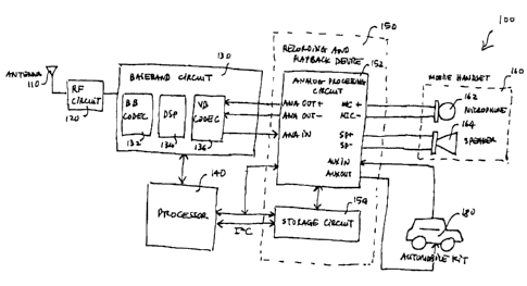
figure 1 i.s a diagram illustrating an exemplary system 100
inr_:or.yorati.n~~ a recording and playback system according to one
<_:mbodiment of the present invention. The exemplary system 100
a.:~ ,_z mobile communication system. However, in other
20 e~nt~odirnents, the recording and playback system rnay be
incorporated in, for example, telephone answering machines,
cor.c7less telephones, personas recorders, etc., to name a few.
The system 100 includes an antenna 110, a radio fret;uency (RE,)
circuit 120, a baseband circuit 130, a processor 190, a
7.5 recording and playback device 150, a mobile telephone handset
160, and an automobile kit: 180.
The antenna 110 receives and transmits RE' signals. The RE
circuit 120 performs RF signal, processing such as down
conversion, filtering, and power amplification. The bas~band
20 circuit 130 performs signal processing functions at the baseband
frequency. The baseband circuit 130 includes a baseband
coder/dec:oder (BB CODEC) 132, a digital signal processor (DSl~)
131, and a voiceband coder/decoder (VB CODCC) 136, The BB CODEC
132 intet;faces with the RF circuit 120. The pSP 139 performs
25 digital signal processing functions on the baseband signals from
the F~E~ CUDEC 132 and VS CODEC: 136. The VE3 CODFC 136 interfaces
012236.P05~ -8- RWB/TVN/rd
E:~press ;l.si1 No.: EL966333695U5 Patent Application
CA 02335195 2001-02-09
h~~;B-D8-2001 'I'HU 04:33 PM BST&Z-LA FAX N0, 310 820 5988 P, 14
wiC,h the recor:d~.ng and playback device 150 for receiving and
transmitting voice band signals, Analog~to-digiCal and digital.-
to-analog conversions are performed at appropriate places in the
b~l5n~'J~'lrlC:~ circuit 1,30.
The: processor 190 communicates with the basehand circuit
and the recording and playback device to perform a number of
Luncl,ions such as control, monitoring, and configuration. The
pr.oc~ssor 140 is typically a microcontroller with sufficient
program and data storage.
fhe recording and playback device 1S0 iS atl analog and
dxgi.tal subsystem that performs various analog signal processing
functions, analog recording, analog playback, and digital
storage. 'rhe recording and playback device 150 includes an
analog processing circuit 152 and a storage circuit 159_ In one
embodiment, the recording and playback device 150 is irnplemented
ire a s ingle integrated circa z.t .
'fhe analog processing circuit 152 provides analog outputs
(AN~1 OUT+ and ANA OUT-), an analog input (AN11 IN), microphone
outputs (MTC+ and MIC-), speaker outputs (SP+ and Sf-), an
au:~iliary output (AUX OUT) and an auxiliary input (AUX IN). The
ANA OUT~+~ and ANA OUT- are coupled to the microphone inputs (MIC
IN-~~ and MIC IN,) of the baseband circuit 130. The 11N~1 IN is
coupled l.o the speaker output (either SP OUT-H or SP OUT-) of the
baseband circuit: 130. The mobile telephone handset 160 includes
a microphone 162 and a speaker 164. The MIC+ and MTC- are
U42236.P058 -9- RWE3/1'VN/rd
E:<pte.~. Moil No.: E,L4F6333645U5 Patent llpplication
CA 02335195 2001-02-09
~u u~ cuv 1 1 nu u4~ J4 ~i I DJ I O:G-Lt1 hH?S NU, 310 ~i20 b9~iti P, 15
coupled to the mirrophooe 162 and the SP+ and SP- are coupled to
Lhc: speaker 164. The F1UX TN and AUX OUT are interfaced to Lhc;
automok~i.le ki.t 1~0. The automobile kit 180 is Chc base portion
c~f a rnobi.le communication system that is installed in a vehicle,
Hy way of example, a user may communicate to a remote caller by
u:i,ng the handset 160 or alternatively, the automotaile kit
interface 180. As herein descra.bed, downstream refers to
Cc~rrIfIlUIIlCcZtion originating from a remote locaCion Chat is
ruc;ea.v~d from the antenna 110, through the baseband circuit 130,
lU anc! to the device 150. Qn the other hand, upstream refers to
communication originated from the handset 160 or the automobile
H;it interface 180, through the basebnnd circuit 130, the antenna
.7.10, and to the remote location. The analog processing circuit
l5?.. i.ncludes analog circuitry Chat provides multiple input and
15 ouLE~ut paths, core analog processing sections, and volume
control circuit. In one embodiment, the analog processing
circuit 152 is described in the co-pending United States Patent
Flpplical:ion Serial No. 09/1x4, ~15~1 entitled "A multilevel message
multilevel analog signal recording and playbar_k system
20 containing configurable analog processing functions", filed
Novernber 2, 1998, assigned to the assignee of the present
invention.
The storage circuit 159 stores analog and di.g:.tal data.
The storage circuit 159 is interfaced to the analog processing
2.5 circuit 152 and the processor 190. The storage circuit 7.59
stores analog data as processed by the analog processing circuit
~9Z236,P058 -l0- RW8/TVN/rcx
G:cpr~ss Mail No.: E;L466333695US parent Application
CA 02335195 2001-02-09
a uu cuu 1 i nu u~r ~ ~4 w r oa r ac,-r.n r H?S IVU, U 1 U tSCU bUtiti P, 16
152, and digital data as transferred from the processor 190 via
a c.onunun.i,cat ion inter face to be described in more detail later _
The communication interface allows the processor 190 Lo exchange
~i.nrormat.i.on with the recording and playback device 150.
t:xamples of the information are commands, status, data, and
adcJresses.
Figure 2 is a diagram illustrating the storage circuit: 154
«C C'ir~ure 1 according to one embodiment of the present
.irivoution. The storage circuit 154 includes a non-volatile
lU memory array 210, a switching circuit 220, and a communieai:ion
irrtc:rtace 260.
'i,he non-volatile memory array 210 is configured to store
ana7.og data, digit7l data, or both, 'fhe memory affray 210
includes a plurality of storage elements 212. In one
ernbodl.ment, the storage elements are organized on a row by row
loasi.s, 'There is essentially no dz.fference in the internal
str.ticture between the digital memory and analog memory. The
difference is the amount of charge stored in tree memory cell.
For digii:al storage, the memory cell is either fully charged
2U (for one logical state, e.g., LOW) or fully discharged (foz
another l.og,ical state, e.g., HIGH) . k'or analog storage, the
~rnourW of charge is between the fully charged and the fully
discharged amounts according to the amplitude of thH signal.
Data sensing schemes are sirnilar. ~3oth digital and analog
memories are sensed with a source follower configuration_
042236. Pa58 -11- R'RB/1'VN/rd
Express Mail No.: ELR66333645US Patent Ap~licati,on
CA 02335195 2001-02-09
mu uu cum i nu u~+. .7;.i fl l DJ 1 ~G-Lli hH?S IYU, .i 1 U tiLU 5~tib P, 17
The swa.tchi.ng circuit 770 receives and transmits analog and
digitatl data to and from the memory array 210. The switching
c.ircuiC 220 includes a control circuit 230, an analog input
s~le:cl:or 240, and a digital selector 250. The control circuit
?.30 <<ontzols the progz~amming and reading of the analog and
digital data. 'the control circuit 230 includes an input/output
out Ciple;~er 232 and a program/read ci.rcui.t 235. The
a,nput:/output mul.tip7.exer 232 is coupled to the memory array 21.0
t_o provide input and output data paths, to steer data from the
rn~~~mdry array 210 to the program/read circuit 235 in the read
cycle, and to steer data from the program/read circuit 235 to
tfvc: «icatory array 210 in the write cycle. The program/read
ci.rcu,it 235 provides control for the programming.and reading of
the tnernory array 210. In the program (or wzite) cycle, the
1'_=~ progr~~m/re~d circuit 235 r~ccives data from the analog input
selector 240 and the digital selector 250 and selects one of the
analog or digit~~l data to transfer to the memory array 2.10
ar_cordi.ng to the control signal, provided by the communication
interface 200, In the read cycle, the program/read circuit 235
provides an analog output Lo the analog processing circuit 152
when operated in the analog mode, and provides a digital data to
the digital selector 2S0 when operated in the digital mode_
The analog input selector 240 rPCeives the analog input
from the analog pz~ocessing circuit 152 and generates an analog
o~.d:pur. to the program/read circuit 235. The analog input
selector 740 includes two sample-and-hold circuits 242 and 244,
0-92236.FD58 -12- RWB/TVN/rd
E;xpres~ Mail PJo.: FT.965333695US Patent e'lpplieation
CA 02335195 2001-02-09
r co uo cuu i t nu u4 ~ ~o rrt ~a t ncc-t.rt h H?S NU, 31 a ~~U b~~ti P, 18
~3nd an analog mults.pl.exPr 246. The two sample-and-hold circuits
297 and ?~14 operate in an alternative mode so t~wt data
1_ransfers to the memory array 210 can Lake place without delay.
'L'he znolog multiplexes 246 sc:lecLs one of the outputs of. the two
santpl.e-and-hold circuits 242 and 294 t,o send t;o the program/read
circuit 235, '!'he analog multiplexes 246 may be replaced by a
).~i.~ff,ering circuit that enables one of the outputs of, the two
sample-anc!-hold circuiCs 292 and 299 at the appropriate taming
insCanCs. The operation of the analog ,input selector 240 is
under conr:rol of the control signal sent from the communicata.on
interface 260. During analog programming, both the analog znput
selector 210 and the registers 252 and 259 are used.
The digital selector 250 is coupled to the communication
interface 260 and the program/read circuit 235 and operates in
rear! and write cycles. The digital seleceor 250 is controlled
by a cotnmand from the communication inlerLace 2i0. In the write
cycle, the di.g~.tal selector 250 receives the serial data from
l.tte comrnunication interface 260 and generates parallel digital.
d~~t~~ to the program/read circuit 235. In the read cycle, the
digital selector. ?.50 receives the parallel digital data from the
prograrn/read circuit ?.35 and generates serial data output to the
communication interface 260. The digital, selector 250 includes
two registers 252 and 254. Each of the registers 252 and 259
can perform parallel-to-serial and serial-to-parallel
conver.sion.s and store data, The two registers 252 and 259
operate in an alternate fashion in both write and read cycles.
092236, P058 -13- RWF~/'I'VN/rd
Ei:press Mail Dlo.: FI~~66333645US PatenC Application
CA 02335195 2001-02-09
r cD uQ CtJU 1 1 t1U U4 ~ 3t7 t'l'1 tfJ i &G-LH FRX N0, 310 820 b988 P, 19
Eor e;;amE~~.e, duxing the write cycle whEn one register is
receiving data Lrorn the communication interface 260, the other
re.c~isCer is available for transferring the previously loaded
data to ttte program/rcad circuit 235, Similarly, during the
rE?r3d cycle, when one register is receiving data from the
program/r~ad circuit 235, the other register' is available for
sending dal:a previously read from the progzarn/read circuit ?.35
to the communicat i.on .inter~ac:e 260.
'Che communication interface 260 is coupled to the memory
1,0 ar.r.~~y 7.10, the analog processing circuit 152, and the switching
circuit 220 to allow the processor 190 Lo e:~change information
with the device 150. The corrununication interface 260 provides a
means For the processor 190 to send command, control,
configuration information and digital data to the device 150 and
to receive the status and the addressed contents of memory array
21,0, The communication interface 260 includes a serial port 268
and othri_ buffering devices.
'The serial poz~t 26~ is coupled to the processor 140 (Figure
1) for transferring serial data accprding to ~ serial
?.0 corrununication protocol. The serial data includes the
information. In one err~~odiment, the serial corrununication
protocol follows an I2C interface_ The IzC interface is
described in the document titled "The IZC--bus specification,
Version 2.0" published by Philips Semiconductor in December
1993. The information includes a command, a data, and a status.
042236. P054 --1a- RwB/TVN/rd
Fpxe:~s Mail No,; EL966333645US Patent Application
CA 02335195 2001-02-09
« .u uu gum mu u~t ~ a i m Des ~ aG.--L,n 1'HlS (VU. J 1 U bCU 5'J'tS~
Figure 3 ~,s a diagram illustrating a memozy organization
300 af. the memory array shown in Figure 2 according to one
embodirncnt; of the present invent~.on. i'he memory array is
orC3.1f11GCG~ as P blocks. Each block includes N rows of storage
'~ ~lemr.~nLs . Each row includes L scans , Each scan corresponds t,o
M-bit data. The contents of a row are either analog or digital
and are detorrnined by the instruction, or opcodc, at the time
tt~c data is written as will be described latei. Typically, tkie
processor. 1.40 (figure 1) keeps track of what is analog and what
is digital in a messages address table as part ox a memory
management scheme.
for analog storage, each row is addressed by log7N bits of
address date. Each row is further dzvided into K groups where
each group includes L/K scans. In each tow, there are K end of
message (EOM) positions, i.e., for each L/K scans, there is an
EOM position at the end. Thus, whion recording, the anaJ.og
recording stops at any one of the L/K positions. In one
crnbodiment, P j 64, N = 2.048, L = 32, M = 64, and K = Q. L'or a
sampll.ng rate of 8 KHz, each row contains 256 milliseconds
(rnsec) of. analog signal (e.g., audio). This also results in a
resolution of 32 msec when ending an analog recording,
L3eginning an analog recordl.ng is limited to the 256 msec
resolution provided by the 11-bxt address,
1:'or digital storage, in addition to the logZN bits for row
addressing, five more bits of address data are needed to address
r_he individual dp.gital scans. Therefore, 16-bit address data is
U9223F.P05~3 -15- RWB/TVN/rd
Express Ma.i.l No.: EL966333645US Patent Application
CA 02335195 2001-02-09
r C.tj u~ LUU 1 I tiU U4 ; ~ r rr~ ~~ I ~~-L8 FAX N0, 310 820 5988 P, 21
used to address a storar~~ Location and each location corresponds
to ,zn M-bit digital data.
figure 4 is a diagram illustrating basic communication
scc~u~ncc:s EJetween the processor 140 and the recording and
~~ playback device 150 shown Figure 1 according to one embodiment
of tt~r~ present invention.
Tl~c recording and playback device 150 is a slave i.n a
::~y:~ecrn having mua.tiple slaves connecting to the cornmurni.cation
bu:; interface of the processor 140. In such a System, each
sl_~3ve is assigned an address, referred to as a slave address,
5hc:wn as slave address 410. In one embodiment, the slave
address 410 includes 7 bits. Tile five most significant address
biCs era fixed, e.g., 10000. The least two signiLicant address
tits, 1~1 and A0, are provided by the indi.vzdual recording and
pl.ayk~aek device 150. 'The slave address is typically transferred
in conjunction with a R/W bit to indicate whether the erode, oz
cycle, i~ a read mode o,r a write made. Typically, B bits are
transrerred as a unit, therefore, the R/W bit i~ transferred
togother. with the 7-bit slave address.
70 In one ernbodi.ment, the communication bus interface is the
I'C serial interface. The T2C bus interface is a serial
interface requiring only two wires, a serial. clock (SCL) and a
serial data (SDA)_ The serial information transmitted over the
IBC bus consists of a sequence of data. The ma ter (e.g., the
pzocessor 140) and the slave (e. g., the recording and playback
042235. P050 -16- RWr3/~L'VN/rd
E:c~~rtas Mail L3o.: E1,~~6f333645U5 Patent Applit,~tion
CA 02335195 2001-02-09
r c.n uo cuu i i rtu u4 ~ 3a rn tsa i ~~-~H hH7S NU, :i i U ti~0 59b~i f,
device 150) communicates with Qach other through a number of
handshakicig signals, conditions, or tokens. From l:he master to
~l~~ve, the conditions inc7.ude a START (S) condition, an
acknowledgment to slave (A TO S), a STOP (P) condition, an Q-bit
I~A'1'A (DATA TO S) transfer, a READ (R) bit, a WRITE (W) bit, and
a NO ACF~ (N) bit. The R bit is a logical 1 in the R/W bit and
tfw~ W bit is a logical 0 in the R/W bit. From the slaves to the
master, the conditions include an 8-bit DATA (DATA L'ROM S)
transfer, and an acknowledc~ccicnC from slave (A FROM S) .
figure 4 illustrates three typical communication sequences
between the processor 190 and the recording and playback device
150: a read status sequence 420, a load single command byte
seduence 430, and a load command byte with address sequence 440.
In tW : Following descrl.pti.on, the term "host" refers to the
~5 master (e.g., the processor 190), and the term "slave" refers t,o
the sl~~vo in the system (e. g_, the rECOrding and playback device
150)
'.l'he zead status sequence 920: The read status is a read
request from the host to the slave without delivering a command
byte. The host supplies all the clocks (SCL). In each case,
the entity sending the data drives the data line (SDA). The
read status command is executed by the IZC sequence 420_ The
sequence 420 includes S (420a), SLAVE ADDRESS (920b), R (420c),
l~ ERC)M S (920d) , DATA FROM S (420e) , A '1'O S (420f) , DATA FROM S
(420g) , A TO S (420h) , DATA 1:'ROM S (420I) , N (920j ) , and P
(420k). The sequence Q20 is explained as follows.
017?36.P058 -17- RWB/TVN/:d
Expz~e~~~ htai.l No, : EL466333695US Patent AF~plicati,on
CA 02335195 2001-02-09
m.u vu mu mm u-r~uu ", uu,~t_, l.,,t rnn ~ru. J1U OCU ~JC3C7
1. fIost executes an I2C START (420a)
2- Host, sends slave address with k/W bit = "1" for RE:~1D
( ~I20b, 920c) .
3. Slave responds back to host an acknow7.edge (ACK)
fol,l.owed by an f3-bit status word 422 (4204, 420e) ,
9- Host sends an acknowledge (ACK) to slave (420f).
Wait for SCL to go (lZGti.
6. Slave rosponds with a high address byte 424 of
internal address register (~f20g).
7. Host: sends an acknowledge (ACK) to slave (42oh).
8. Slave responds with a low address byte n26 of internal
address regisCer (420i).
9- Ffost sends a NO ACK to sJ.ave, and then r,~recutes an T2C
STOP (420j, 92ok).
Note that the host could have sent an after the Status word
data t:ransFer and aborted the transfer of the addzess bytes.
Load single command byte sequence 430: 11 single byte may be
written to the command byte register in order to power up the
device, start or stop the analog record (if no address is
rueeded), or do a message cueing function. The sequence 430
includes S (430a), SLAVE ADDRESS (930b), W (430c) A FROM S
(930d), DATA TO S (930e), A FROM S (430,f), and P (930g). The
scc~uencc 930 is erplained as follows.
1. Host executes an IZC START (430x),
2. Host sends slave address with R/W bit = "0" for WRITE
(930b, 430c).
047.236. P05F3 -18- RWB/TVN/rd
G:<pre;s Moil Nv.: EL466333695US Patent Application
CA 02335195 2001-02-09
. a.u vv Lvv1 lIIV VT~TV 1 JI VIJI~iC. L11 f'!"IA IYV. J1U UCU 0~7C1CS f'.
3. Sl~wo responds back to host an acknowledge (ACK) (430d) .
9. I-Post sends a command byte X132 to slave (~130e) .
5. Slave responds with an acknowledge (11CK) (430f).
6. Host; executes an TZC STOP (430g) .
Load command byte with address sequence 940: Tt>c: lead
scquEnce
990 provides
the normal
addressed
mode. The
sequence
~I~10 includes
S (490a)
, SLAVE
ADDRESS
(~140b)
, W (WOc)
, A FROM
S
(d~lOd) , nA'1'A fO S (940c) , ~1 FROM S (490f) , D11T~1 TO S
(990g) , 11
CROM S (Q40h) , D11T11 TO S (490i) , A FROM S (940j ) , and
P (990k) .
'1'hc uence n90 is explained as follows.
seq
1. Efost executor an IzC START (930a).
2. Host sends slavo address with R/W bit ~ "0" for WRITE
(~190b, 990c) .
3. Slave responds with an acknowledge (ACK) (940d).
4. Host sends a command byte 932 to slave (490e).
S. Slave responds with an acknowledge (ACK) (440f).
6. i-fort sends a high address byte 494 to slave (440g).
7. Slavo responds with an acknowledge (RCK) (490h).
8. Host sends a low address byte A46 to slave (990i).
9. Slave responds with an acknowledgo (ACK) (490j).
10. Host executes an z~C STOP (A40k).
In the IzC write mode, the device can accept data sent
after Lhe command byte, zf a register load option is selcct:ed,
the next two bytes are loaded into the selected regzster. The
~5 format of the data is MSt3 first. Thus, to load DRTA<15:0> into
the device, DRTA<15:8> is sent first, the byte is acknowledged,
042?..36.P058 -19- RWB/TVN/rd
F:cpr.ess Mail No,~ EL966333695US P,stcnt Application
CA 02335195 2001-02-09
.~ w ~vvi ,..v v-r~-ri i m ur.mc. Ln rnn 1'IU. Jlu CSCU ~JCSCS Y. Cl
anci DATA<'7:0> a.s sent next. The address register consists of.
two bytes with the following format:
Af)l7f~E:SS<a.5:0> -~ ROW ADf7RFSS<10:0>, SCAN ADDR~:SS<4:0>
Ii nn analog function is selected, the scan address bits
arc ic3c~orcd. Notc that digital rcad and write arc scan
addressable.
figure 5A is a diagram illustrating format of. the status
word X122 shown in Figure 4 according to one embodiment of the
E~rc:sent invcnCion. When the slave (e.g., the recording and
7.0 p7.ayhack device 150 in Figure 1) is polled with the read status
command a,s iJ.lustzated in E'igure 9, it returns three bytes of
data. The first byte is the status byte, the next is the upper
address bytc, and the last is the lower address byte. The
sl:aLus word 422 includes an end of message (EOM), an ovorflow
(nVF), a randy (READY), a power up (PU) condition, a play/record
mode indicator (PftH) , and a devzce identification (D~:VICE. Ifa) .
The EOM bit indicates whether an EOM interrupt has
occurred. The OVg~ bit indicates whether an overflow interrupt
has occurred. The READY bit indicates the internal status of
the device. If RElIDY is LOW, no new commands should be sent to
ttic device. The PU bit indicates if the device is powered up
(fU = HICH). ~'he PRB indicates if the device is in a play mode
(fRl~ - HIGH) or record mode (PRB ~ LOW). The DEVICE XD is 3-bit
and indicates the internal device ID, which is a pre-defined bit
pal:Lern (e. g. , 001) .
042236.?05~ -20- RH1B/TVN/rd
Express Mail No.: EL466333645US Patent Application
CA 02335195 2001-02-09
---- _~ ~.-... ",~ ~" ~ vv , m uv "iG. LI I r nn ivu, 01 U tSCU SdtStS t', U t
Figure SB is a diagram illustrating formal of the command
word 4.32 as shown in Figure 4 according to one crnbodirnent of the
present invention. The command word 432 is used to control the
dov~.ce. 'i'he command word 432 is sent after the 7-bit device
adctt:'ess and the 1-bit Read/Write selection bit as illustrated in
t'igttro ~1. The command word 932 includes a power up bit (PU),
~jigit~il analog bit (DI~n) , three function bits (FN2, FN7., and
CNO) , and three register bits (RG2, I~G1, and hG0) .
'T'he PU bit is usedto provide global power up. The DAB
bit,
1,0 is used 0 CUIltrol evice to perform an analog or a digital
t the d
furtcti.on. fhe FN2-FNO
bits are used
to specify
which function
ttye devic es is to performin conjunction with the DAB bit_ The
RG2-RC;O t its are used specify it and when data ~.s l.o be
to
loaded to a register.
Those bits
are used as
follows.
DAa fN2 FN1 FNO Function
0 0 0 0 STOP (or do nothing)
0 ~- 0 1 Analog play
0 0 1 0 Analog record
0 1 1 1 Analog message cue
20 1 1 0 0 Digital read
I 0 0 1 Digital write
1 0 1 0 Digital erase
Tho register load stay be used to modify a command sequence
(such as load an address) or used with the null command sequence
25 to load a configuration or test register. Not all registers are -
accessible to the user.
09??36.P058 -21- RWB/TVN/rd
C~pr~..,s ~9ai1 tJo.: EL466333645US PatenC Applicat:.on
CA 02335195 2001-02-09
.... _.. ".... ,.", ,... ,.,. ", ""m~ w rnn ivu, mu ocu o~tfo r', UC
EtG2 RGl RGO Description
0 No aCtlOtl
0 a. Load address
0 1 0 Load configuration rega,ster 0 (CFGO)
0 1 1 Load configuration register 1 (CFG1)
Digital write; The digital write function allows the user
l:o sQlcct a portion of the memory array to be used as digital
monot~y. The partition between analog and dig~.tal memory is left
up to the user. A row can either be digital or analog, but not
both. rn one embodiment, the minimum addressable block of
~necnory is one scan or 6~ bits. The address sent to the device
is the 11-bit address row (or page) address with the 5-bit scan
(oz' block) address. After the address i.s enCered, the data is
sent in one-byte packets followed by an I2C acF:nowlcdge
1~ gooerated by the device. pal:a for each block is sent with MSB
first. The data transfer. is ended when the master (e.g., the
~~L~oc:essor, 190 in figure 1) generates an I2C S'I.~UP condition. zf
only a parCiai block of data is sent before the STOP condition,
zero is "written" in the remaining bytes; that is, they are left
at the erase level. An erased page (or row) is road as all
zeros. The device can buffer up to two blocks of data_ If the
d~vic:e is unabJ.e to accept morn data due to the .internal write
process, the SCL line on the serial bus wzll be held low
indicating to the master to halt the data transfer, for a 32
?.5 rn~ec cycle, the sustained write rate is 2 Mbits/s. If the
device encounters an overflow condition, it responds by
042236.P058 -22- RWB/TVN/rd
Eaprcs~ Mail c7o.: FLh66333645US Patent Application
CA 02335195 2001-02-09
m.u vv gum my u~ ~ ut i 11 pJ I OtL-Lf1 t'Hn 1VU, ,i1 U tSLU b'~tSb N,
genPraLing an interrupt condition and an IBC Not Acknowledge
SicJnal afCer the last valid byte of data. Once data transfer is
tPrrninated, the device needs up to two cycles (69 msec) to
comF~leta its internal write cycle before another command is
p ~eut. If an active command is sent before the internal cycle is
Finished, the device will hold the SCL line low until the
current command is finished,
l1 sequence to write data to the slave device from the host
a.s as fol lows .
1. Host executes an I2C STACtT
2, Host sends slave address with R/W bit = 0 for WRIT;
Slave responds with an ACK
4. Wait for SCL HIGH
5. Host sends a command byte to slave
G, Slave responds with an ACK
7. Wait for SCL HIGH
a, (lost sends high address byte tc slave
9. Slave responds with an ACK
10. Wnit for 5CL I~IGH
11_ (lost sends low address byte to slave
12. Slave responds with an 11CK
13. Wait for SCL HIGH
14. Host sends data byte to slave
7.5. Slave responds with an RCK
16. Wait for SCL HIGH
042236,p058 --23- RWI3/TVN/rd
express Mail No.; EL46o333695US Patent App=ication
CA 02335195 2001-02-09
.. ~..... ..~" ..,. ". ", ~.,"~~, ~n rnn iru. ~1u bCU 5abu t'. 04
17. Steps 1~1, 15, and 16 are repeated until the la:;t byte
.i.s send and acknowledged.
Uigil.cll read: The digital read command utilises a combined
I~C corrunand format. In this combined formal, a command is sent
to the slave device (e.g., the recoz~d and playback device 150
shown in Eigure 1) using the write data direction, then the data
direc:ti.on is reversed by sending a repeated start condition,
which consists of a repeated staz~t, and the slave address with
R/W set to 1. After this, the device begins to send data Lo the
7.0 rna.sl.er until. the master generates a Not Acknowledge. If Lhe
dev,i.ce encounters an overflow condition, an interrupt is
generated.
n typical sequence for a digital. read from the slave device
is as follows.
1~ 1. , llost executes an I2C START
2. itost sends slave address with R/W bi.t = 0 for WRITE
3. Slave responds with an ACK
'd. Host sends a command byte to slaves
a. Slave responds with an ACK
20 6. lost sends high address byte to slave
7. slave responds with an ACK
e. Host sands low address byl:e to slave
9. Slave responds with an ACK
10. Host sends another IzC START
2S 11. Host sends slave addxess with R/W bit = 1 (Reverse
data direction)
04223G.P0~8 -29- RWB/TvN/rd
Express Mail No.; EL966333645US Patcnt Application
CA 02335195 2001-02-09
.. . .. .,._ . _.. .... 1 1111 IYU, J 1 U UGU :JO00 (,
12. Slave responds with an ACK
13. Slave sends a data byte to host
1~- Host responds with an ACK
1'' Step 12 ~~nd 13 are repeated until the last byte is
sent and acknowledged
16. Host executes an I'C STOP.
While certain exemplary embodiments have been described and
shown i.n i~he accompanying drawings, it is to bo understood that
such emboditnents are merely illustrati~r~ of and not restrictive
on the broad invention, and that this invention not be limited
to the specific constructions and arrangements shown and
C~GSC1: i.bed, since various other modifications rnay occur to those
ordinarily skilled in the art.
D92236,pO5Q -25- RWB/TVN/rd
Rxyres~ Mail tto.: EI,9G6333645US °atent ApplS.cation
CA 02335195 2001-02-09