Note: Descriptions are shown in the official language in which they were submitted.
CA 02335430 2000-12-15
WO 00/68731 PC'T/US00/12397
External Optical Modulation Using
Non-Co-Linear Compensation Networks
Field of the Invention
The invention relates generally to the field of optical modulation and, in
particular,
to methods and apparatus for high-speed external optical modulations.
Background of the Invention
Optical modulators impress or modulate RF (or microwave) electrical signals
onto
a light beam in order to generate a modulated optical beam that carries data.
Modulators
1 o either directly modulate the optical beam as it is generated at the
optical source or
externally modulate the optical beam after it has been generated. Direct
modulation is
typically accomplished by modulating the drive current of the optical source.
An
integrated electro-absorptive modulator can modulate the optical intensity of
light leaving
the source as well.
15 External modulation can be accomplished by using an external modulator that
is
separate from the optical source. External modulation is advantageous because
it can
modulate signals over a very wide bandwidth. External modulators are typically
voltage-
controlled devices that include a traveling-wave electrode structure, which is
positioned in
close proximity to the optical waveguide. The electrode structure produces an
electric
2o field that overlaps the optical waveguide over a predetermined distance
(the interaction
length) and causes an electromagnetic interaction which modulates the optical
signal.
Lithium niobate (LN) electru-optic external modulators are increasingly being
used
to modulate data on optical signals that are being transmitted at very high
data rates and
over long distances. Lithium niobate modulators are advantageous because they
can
25 modulate optical signal over a broad frequency range, they modulate optical
signals with
minimal optical frequency shift (frequency "chirp"), and they operate over a
broad
CA 02335430 2000-12-15
WO 00/b8731 PCTNS00/12397
2
wavelength range. These features are particularly desirable for Dense
Wavelength
Division Multiplexing (DWDM) broadband optical communication systems that
transmit
optical signals with many optical wavelengths through a single optical fiber.
Modulators used for transmission at high speeds and over long distances must
be
s efficient to avoid the use of expensive electronic amplifiers and digital
drivers. In addition,
modulators need to be compact in order to minimize the required space on the
transmitter
card.
Lithium niobate crystals have an inherent mismatch between the velocity of
optical and electrical signals propagating through the crystal which impacts
modulation
efficiency. The RF propagation index is significantly higher than the optical
refractive
index of lithium niobate. That is, the lithium niobate crystal slows the RF
signal relative
to the optical signal so that it takes the RF signal a longer period of time
to travel over the
interaction distance. Thus, the RF signal becomes out-of phase with or "walks
ofi?' the
optical signal. Consequently, the modulation becomes inefficient. The longer
the
l s interaction distance. the greater the inefficiency. Using a buffer layer
can minimize
velocity walk-off. however, the required interaction length is long.
Fig. 1 illustrates a top view of a prior art electro-optic device 10 that
compensates
for the velocity mismatch between the optical and electrical signals
propagating through
the device by using phase reversal sections that are co-linear with the
optical waveguide.
2o The device 10 includes an optical waveguide 12 and RF electrodes 14 that
are positioned
in zero degree phase sections 16 and in phase reversal sections 18. The phase
reversal
sections 18 periodically flip the RF electrodes 14 to either side of the
optical waveguide
12 to produce a 180 degree phase shift in the RF signal relative to the
optical signal. The
RF electrodes 14 are positioned to alternate between the zero degree phase
shift sections
25 16 and the 180 degree phase shift sections 18. The length of the zero
degree phase shift
sections 16 is chosen so that the RF signal "walks off ' the optical signal
approximately
180 degrees before it is flipped 180 degrees in the phase reversal sections
18.
CA 02335430 2000-12-15
WO 00/68731 PCT/US00/12397
Fig. 2 illustrates a top view of a prior art electro-optic device 30 that
compensates
for the velocity mismatch between the optical and electrical signals
propagating through
the device 30 by using co-linear but intermittent interaction sections. The
device 30
includes an optical waveguide 32 and RF electrodes 34 that are positioned to
alternate
s between an interaction region 36 arid a non-interaction region 38 relative
to the optical
waveguide 32. The length of the interaction region 36 is chosen so that the RF
signal
"walks off' the optical signal by as much as 180 degrees of phase shift before
it is routed
away from the optical waveguide 32 in a co-linear direction and into the non-
interaction
region 38. The length of the non-interaction region 38 is chosen so that the
RF signal
t o becomes phase matched with the optical signal at the end of the non-
interaction region 38.
One disadvantage of prior art electro-optic devices that compensate for the
velocity mismatch between the optical and electrical signals propagating
through the
device is that they have relatively low modulation efficiency per unit length.
This is
because the phase of the RF signal is modified with co-linear sections that
are positioned
t > at intervals of 180 degrees. When the difference in phase between the RF
and optical
signals approaches 180 degrees, the incremental increase in modulation depth
with
incremental change in electrode length approaches zero. Therefore, the total
length of the
device must be increased in order to achieve the required modulation.
Increasing the length
of a lithium niobate device increases the size of the package containing it,
which is
20 undesirable, because of the limited space on the transmitter board. State-
of the-art
DWDM systems have stringent space requirements due to their high channel
count. In
addition, more expensive and larger power supplies must be used because higher
drive
voltages are required.
Summary of the Invention
25 It is therefore a principal object of this invention to provide an electro-
optic device
that includes a compensation network that modifies at least one of the phase
or the
amplitude of the electrical signal relative to the phase or amplitude of the
accumulated
modulation on the optical signal without introducing significant loss or
decreasing the
CA 02335430 2005-06-21
4
modulation efficiency. It is another principle object for such a compensation
network to
compensate for velocity mismatch between the electrical signal and the optical
signal. It
is another principle object for such a compensation network to compensate for
the effects
of external perturbations in the substrate of the modulator, such as the
effects of
temperature on a lithium niobate substrate. It is another principle object for
such a
compensation network to be removably attached to the device to facilitate
modifying the
frequency response of the device. It is yet another principle object of the
present
invention to construct a modulator with such a compensation network that is
used in
conjunction with prior art broadband modulator to form a combined modulator
that is
capable of producing bandwidth extension of the broadband modulator into the
narrow
band modulator region.
A principal discovery of the present invention is that an electro-optic device
can
be constructed with a compensation network that temporarily directs the
electrical signal
in a path that is in a non-co-linear direction relative to the direction of
propagation of the
1 S optical signal and that such a compensation network has numerous
advantages over the
prior ;art. For example, such a compensation network can modify the phase of
the
electrical signal relative to the optical signal in order to minimize the
effects of velocity
mismatch, while introducing very low loss. Such a compensation network can
also
compensate for the effects of external perturbations on the electro- optic
device. In one
embodiment of the invention, such a compensation network is used to construct
a
modulator that provides more efficient modulation per unit length of
electrode.
Accordingly, the present invention features an electro-optic device that
includes
an optical waveguide that is formed in an electro-optic substrate such as
lithium niobate.
The optical waveguide propagates an optical signal along a first direction of
propagation.
An electrical waveguide is also formed in the electro-optic material and is
positioned co
linear relative to the optical waveguide and in electromagnetic communication
with the
optical waveguide. The electrical waveguide also propagates an electrical
signal in the
first direction of propagation.
n I f f f
CA 02335430 2005-06-21
In addition, the electro-optic device includes a compensation network, formed
on
a separate substrate, which is electrically coupled to the electrical
waveguide at a
junction. The compensation network propagates the electrical signal in a
second direction
of propagation that is substantially non-co-linear with the first direction of
propagation.
5 In one embodiment, the compensation network includes at least one of an all-
pass
electrical network, an inductor- capacitor "Pi" network, traveling wave
coupler, filter, and
transmission line transformer.
The compensation network is designed to modify at least one of the phase or
the
amplitude of the electrical signal at the junction relative to the phase or
the amplitude of
the accumulated modulation on the optical signal at the junction,
respectively, forming a
modified electrical signal, and then return the modified electrical signal to
the electrical
wavel,Tuide. The compensation network may be a time delay network or a phase
delay
netwalrk.
In one embodiment, the compensation network is a phase delay network that
modifies the phase of the electrical signal so that an electro-optic response
of the device
is increased. In another embodiment, the compensation network is a phase delay
network
that modifies the phase of the electrical signal so that an electro- optic
phase at the
junction is substantially equal to an electro-optic phase at an input of the
electrical
waveguide.
In yet another embodiment, the compensation network is a phase delay network
that modifies the phase of the electrical signal at the junction relative to
the phase of the
accumulated modulation on the optical signal at the junction by a
predetermined delay
that is variable over a range from zero to one hundred and eighty degrees. In
this
embodiment, the phase of the electrical signal at the junction relative to the
phase of the
accumulated modulation on the optical signal at the junction may be modified
to be
substantially one hundred and eighty degrees.
One advantage of the compensation network of the present invention is that the
electrical loss per unit length can be designed to be significantly lower than
the electrical
loss per unit length of the electrical waveguide to minimize RF losses.
Another advantage
CA 02335430 2000-12-15
WO 00/68731 PCT/US00/12397
of the compensation network is that it may be removably attached to the
electro-optic
device so that it can be replaced by another compensation network with
different
characteristics. Another advantage of the compensation network is the
temperature
dependence of the compensation network can be made to be inversely
proportional to the
temperature dependence of the electro-optic material so as to compensate for
temperature
non-linearity in the electro-optic material.
The present im ention also features an electro-optic modulator that includes a
plurality of compensation networks. The optical waveguide is formed in an
electro-optic
material such as lithium niobate. 'the optical waveguide propagates an optical
signal along
o a first direction of propagation. An electrical waveguide is formed in the
electro-optic
material and is positioned in a co-linear direction relative to the optical
waveguide and in
electromagnetic communication with the optical waveguide. The electrical
waveguide also
propagates an electrical signal in the first direction of propagation. Each of
the plurality
of compensation networks are electrically coupled to the electrical waveguide
at one of a
~ 5 plurality of junctions. Each of the compensation networks propagates the
electrical signal
in a second direction of propagation that is substantially non-co-linear with
the first
direction of propagation.
In operation. each of the plurality of compensation networks modifies a phase
of
the electrical signal at a respective junction of the plurality of junctions
relative to a phase
20 of the accumulated modulation on the optical signal at the respective
junction by a
predetermined delay and then returns the modified electrical signal to the
electrical
waveguide. The predetermined delay is variable over a range from zero to one
hundred
and eighty degrees and, in one embodiment of the invention, the predetermined
delay is
substantially one hundred and eighty degrees. In another embodiment, each
compensation
25 network modifies the phase of the electrical signal at the respective
junction relative to the
phase of the accumulated modulation on the optical signal at the respective
junction so
that an electro-optic response of the device is increased.
CA 02335430 2000-12-15
WO 00/68731 PCT/US00/12397
7
Brief Description of the Drawings
This invention is described with particularity in the appended claims. The
above
and further advantages of this invention may be better understood by referring
to the
following description taken in conjunction with the accompanying drawings, in
which:
Fig. I illustrates a top view of a prior art electro-optic device that
compensates for
the velocity mismatch between the optical and electrical signals propagating
through the
device by using phase reversal sections that are co-linear with the optical
waveguide.
Fig. 2 illustrates a top view of a prior art electro-optic device that
compensates for
the velocity mismatch betty-een the optical and electrical signals propagating
through the
to device by using co-linear but intermittent interaction sections.
Fig. 3 illustrates an electrode cross-section of a prior art traveling wave
electro-
optical device where the optical and electrical signals propagate in an
entirely co-linear
path.
Fig. 4 illustrates a top view of a segmented electro-optic device according to
the
~ 5 present invention that includes a compensation network where the
electrical signal
propagates in a non-co-linear path relative to the optical signal.
Figs. Sa-c illustrate vectorial representations of the electro-optic response
of a
prior art non-velocity matched modulator having three electrode lengths: L;
2L; and 3L,
respectively.
2o Fig. 6 illustrates a vectorial representation of the electro-optic response
of a non-
velocity matched modulator of the present invention that modifies the
modulation signal
so that the electro-optic response of the modulator is increased.
Figs. 7a-b illustrate a vectorial representation of the electro-optic response
of the
modulator of the present invention having optimal and non-optimal modulation
efficiency,
25 respectively.
CA 02335430 2000-12-15
WO 00/68731 PCT/US00/12397
Fig. 8 presents a graph comparing the theoretical modulation efficiency for: (
1 ) a
segmented electro-optic modulator according to the present invention; and (2)
for an
optimized non-velocity matched prior art modulator.
Fig. 9 presents a graph comparing the theoretical modulation efficiency of a
segmented electro-optic modulator according to the present invention with two
optimized
velocity matched prior art modulator.
Detailed Description
Fig. 3 illustrates an electrode cross-section of a prior art traveling wave
electro-
optical device SO where the optical and electrical signals propagate in an
entirely co-linear
o path. The substrate ~2 is formed of an electro-optic material such as
lithium niobate
(LiNbO;). Many prior art devices use X-cut LiNb03 substrates. The device
includes
optical waveguides 54 that are positioned entirely within the substrate 52.
The optical
waveguides 54 may be formed by diffusing titanium into the LiNbO; substrate
52.
Electrical waveguides are positioned in a co-planar waveguide (CPW) geometry
with a hot
electrode 56 positioned in the center of the CPW structure and ground
electrodes 58
positioned adjacent to both sides of the hot electrode 56. The ground
electrodes 58 are
spaced apart from the hot electrode by a gap 60. Typical prior art device
lengths are on
order of 20 mm.
Optical and electrical modulation signals propagate along the optical 54 and
20 electrical waveguides 56, 58, respectively, into the plane of the page. The
electrical
modulation signal generates an electric field 62 that travels from the hot
electrode 56 to the
ground electrodes 58. It is desirable to minimize the required amplitude of
the electrical
modulation signal. The gap 60 is typically chosen to be small in order to
maximize the
electromagnetic interaction of the electrical waveguides 56, 58 with the
optical waveguides
25 54 and thus minimize the amplitude of the required electrical modulation
signal.
The required amplitude of the electrical modulation signal is determined by
the
switching voltage-length product (Vpi-L) of the device which is a function of
both the
CA 02335430 2000-12-15
WO 00/68731 PCT/US00/12397
9
electrode geometry and the degree of overlap between the electric field 62 and
the optical
signal. Vpi-L of typically prior art devices is typically 40 to 50 Volt-mm for
the CPW
structure shown in Fig. 3. Thus for a device with 20 mm long electrodes, the
required
electrical modulation signal is approximately 2 volts.
A disadvantage of the prior art device 50 is that at high modulation
frequencies,
RF losses become significant. Typical RF losses range from about 0.5 to 1
dB/Sqrt(GHz)-cm for LiNbO_;. Consequently, the electromagnetic interaction of
the
electrical waveguides ~6. ~8 with the optical waveguides 54 decreases at high
frequency
thereby increasing the Vpi-L and thus, the required amplitude of the
electrical modulation
no signal.
Another disadvantage of prior art devices is that the velocities of the
optical signal
and the electrical modulation signal are different. The velocity of the
electrical modulation
signal is determined by the RF propagation index, which may be as high as 3.5
to 4Ø
The velocity of the optical signal is determined by the optical propagation
index, which is
approximately 2.1 for LiNbO~. The difference in the RF index and the optical
propagation index results in a significant velocity mismatch of the optical
and the
electrical modulation signals. This velocity mismatch results in the optical
signal
becoming out-of phase with the electrical modulation signal thereby reducing
or canceling
the accumulated modulation, and increasing the amplitude of the required
electrical
2o modulation signal.
Some prior art devices include a buffer layer 64 that is positioned between
the
electrodes 56, 58 and the substrate 52 that has a lower refractive index than
the substrate
52. Using the buffer layer 64 lowers the RF index because the buffer layer 64
together
with the substrate 52 presents an average effective RF index that is somewhere
between
the refractive index of the buffer layer 64 and the RF index. Using a buffer
layer,
however, degrades the efficiency of the device because the electric field must
penetrate a
longer path and thus is reduced in magnitude.
CA 02335430 2000-12-15
WO 00/68731 PCT/US00/12397
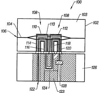
Fig. 4 illustrates a top view of a segmented electro-optic device 100 of the
present
invention. The device includes an electro-optic AM modulator 102 that is
formed on an
electro-optic substrate 103, which in one embodiment is a LiNb03 substrate.
Optical
waveguides 104 are formed in the substrate as described in connection with
Fig. 3 or by
5 numerous other techniques known in the art. An optical signal input 106 of
the optical
waveguides 104 is positioned to receive an incident optical beam. The optical
waveguides
104 split into two paths.
The modulator 102 includes electrical co-planar waveguides 108 that propagate
the
electrical modulation signal along hot and ground electrodes as described in
connection
to with Fig. 3. The waveguides 108 have a first 110 and a second co-linear
section 112
where the electrical modulator signal propagates in a co-linear direction
relative to the
optical signal. The first co-linear section 110 ends at a compensation point
113.
In one embodiment of the present invention, the length of the first and second
co-
linear sections is chosen to be approximately the length where the velocity
mismatch
t 5 between the electrical modulation signal and the optical signal causes a
significant
degradation in the incremental change in modulation efficiency with additional
electrode
length. In another embodiment of the present invention, the length of the
first and second
co-linear sections is chosen to be approximately the length were the velocity
mismatch
between the electrical modulation signal and the optical signal is such that
the electrical
2o modulation signal is one hundred and eighty degrees out-of=phase relative
to the phase of
the accumulated modulation on the optical signal.
The waveguides 108 also have a first 114, second I 16, third 118, and fourth
non-
co-linear section 120 where the electrical modulator signal propagates in a
non-co-linear
direction relative to the optical signal. A modulation signal input waveguide
122 with
25 ground electrodes 123 is electrically coupled to the first non-co-linear
section 114. The
modulation signal input waveguide 122 may be positioned on a separate
substrate as
shown in Fig. 4 or on the modulator substrate 103.
CA 02335430 2000-12-15
WO 00/68731 PCT/IJS00/12397
The electro-optic device 100 also includes a compensation network 124 that is
coupled to the compensation point 113 by the second non-co-linear section 116.
The
compensation network 124 can be designed to provide any type of frequency
response.
In one embodiment of the present invention, the compensation network 124 is
designed
so that its frequency response increases the modulation efficiency.
The compensation network can be implemented by numerous traveling wave and
lumped element structures known in the art such as an inductor-capacitor ''Pi"
network,
traveling wave coupler. filter. and a transmission line transformer. In one
embodiment, the
compensation network 124 comprises a phase delay section that has a length
which
delays the phase of the electrical modulation signal relative to the phase of
the
accumulated modulation on the optical signal.
In one embodiment of the present invention, the compensation network 124 is
designed to generate frequency response characteristics that vary with at
least one external
perturbation in a manor that compensates for such perturbation. For example,
the
~ 5 compensation network 124 may be designed to generate frequency response
characteristics that vary with temperature in such a way as to compensate for
the effect
of temperature variations in the modulator substrate 103. This can be done by
varying
the physical length, dielectric constant, or other parameters of the
compensation network.
In one embodiment of the present invention, the compensation network 124 is
2o positioned on a substrate 126 that is separate from the modulator 102 and
is removably
attached to the modulator 102. Such a feature allows an electro-optic device
to be easily
reconfigured. For example, a modulator of the present invention may be used in
an optical
communication system with variable bandwidth. In such a system, the bandwidth
can
easily be changed by replacing the compensation network with one having the
desired
25 frequency response.
One advantage of the present invention is that the electrode geometry of the
compensation network 124 can be designed to provide much lower loss compared
with
CA 02335430 2000-12-15
WO 00/68731 PCT/US00/12397
12
the electrical co-planar waveguides 108 of the modulator 102. That is, the
electrodes
comprising the compensation network 124 can be constructed with wider
conductors that
have relatively low resistive losses and wider gaps between the conductors
which reduce
skin effect losses. In addition, the compensation network 124 may be formed on
a low-
s loss substrate that is separate from modulator 102. In one embodiment, the
input
waveguide 122 and the compensation network 124 are formed on a ceramic
substrate to
reduce RF losses.
In one embodiment of the present invention, the electrical co-planar
waveguides
108 of the modulator 102 are terminated in a matched impedance 128 that is
attached to
t o the end of the fourth non-co-linear section I20. Terminating the
electrical waveguides 108
will eliminate or reduce reflections. which increase the RF signal returned to
the RF signal
generator connected to input 122. In the embodiment illustrated in Fig. 4, the
matched
impedance 128 is a chip resistor that is attached to substrate 126.
In another embodiment, the compensation network 124 is formed directly on
t 5 modulator substrate 103. 1n one embodiment, the compensation networks are
fabricated
on lithium niobate substrates that may be formed directly on the modulator
substrate 103
or may be formed on a separate lithium niobate substrate. Fabricating the
compensation
network 124 on a lithium niobate substrate is advantageous because lithium
niobate is less
susceptible to parasitic effects, such as parasitic coupling to the package
(not shown). In
20 one embodiment where the compensation networks are fabricated on lithium
niobate
substrates, the width of the hot electrodes within the compensation network is
100
microns or less. Also, in one embodiment, the ground electrodes at the input
are isolated
from those at the output, in order to prevent ground currents from taking a
path that
bypasses the delay line.
25 In another embodiment of the invention, the electro-optic device
illustrated in Fig.
4 is used in conjunction with a prior art device such as the device
illustrated in connection
with Fig. 3. Such a combination results in a combined narrow band and
broadband
CA 02335430 2000-12-15
WO 00/68731 PCT/US00/12397
13
modulator that can be used to produce bandwidth extension of the broadband
modulator
into the narrow band modulator region.
In operation, an optical signal is coupled to the optical signal input 106 of
the
optical waveguides 104 and an electrical modulation signal is coupled to the
modulation
signal input waveguide 122. The optical signal propagates along the optical
waveguides
104. The electrical modulation signal propagates along the first non-co-linear
section 114
of the electrical co-planar waveguides 108 until it merges with the first co-
linear section
I 10 of waveguides 108. The electrical modulation signal then propagates along
the first
co-linear section 110 where the electrical modulation signal
electromagnetically interacts
o with the optical signal. thereby modulating the optical signal.
The electrical modulation signal is then directed away from the optical
waveguides
108 at the compensation point 113 to the second non-co-linear section I 16 of
the
electrical co-planar waveguides 108, which directs the electrical modulatian
signal into the
compensation network 124. The compensation network 124 modifies at least one
of the
t 5 amplitude or phase of the electrical modulation signal relative to the
amplitude or phase of
the accumulated modulation on the optical signal, respectively, and then
returns the
compensated modulation signal to the third non-co-linear section 118 of the
electrical co-
planar waveguides 108. The modulated optical signal is then detected by and
optical
detector (not shown) and then demodulated by a demodulator (not shown).
2o The compensated electrical modulation signal propagating on the third non-
co-
linear section 118 of waveguides 108 merges with the second co-linear section
112 of
waveguides 108. The compensated modulation signal then propagates along the
second
co-linear section I 12 where the compensated modulator signal
electromagnetically
interacts with the optical signal, thereby modulating the optical signal.
25 In one embodiment. the phase of the electrical modulation signal is
modified so
that the electro-optic response of the modulator is increased. By electro-
optic response,
we mean the ratio of the magnitude and phase of the detected output voltage of
the
CA 02335430 2000-12-15
WO 00/68731 PCT/US00/12397
14
modulator to the magnitude and phase of the RF modulation signal. The electro-
optic
response represents the accumulated modulation on the optical signal for
either a section
of the modulator, or the entire modulator. The electro-optic response of a
prior art non-
velocity matched modulator and a modulator according to the present invention
are
vectorially illustrated below.
Figs. Sa-c illustrate vector-ial representations of the electro-optic response
of a
prior art non-velocity matched modulator having three electrode lengths: L;
2L; and 3L,
respectively. The magnitude of the vector represents the strength of the
modulation and
the phase of the vector represents the phase relationship between the input RF
I o modulation signal and the detected output voltage on a photodetector. The
electro-optic
response vector. R~". is defined as the ratio of the voltage generated by a
photo-detector
that detects the modulated optical signal to the RF modulation voltage.
Assuming negligible RF losses, the magnitude of the electro-optic response for
each segment of the modulator is the same. However, the phase of the electro-
optic
15 response (electro-optic phase), which is the RF phase of the accumulated
modulation for
each segment, changes. This is because of a mismatch in velocity between the
optical
signal and the propagating RF signal. That is, the RF signal travels slower
than the optical
mode, therefore. the electro-optic phase change is represented by a counter-
clockwise
rotation of the vector for each individual segment. The greater the frequency
and/or the
2o greater the velocity mismatch, the quicker the rotation of the phase.
Because of the
velocity mismatch, the resultant vector R~° has a magnitude that is
less than the sum of
the magnitudes of the individual vectors.
The magnitude of the response for an electrode length of 2L (Fig. 5b) and 3L
(Fig.
5c) is normalized to the magnitude of the response for an electrode length of
L (Fig. 5a).
25 Fig. 5b illustrates that the electro-optic phase changes by 180°
after 2L of electrode
length. The total electro-optic response of the modulator having an electrode
length of 2L
is only 40% larger than the response of the modulator having an electrode
length of L,
. even though the modulator is twice as long.
CA 02335430 2000-12-15
WO 00/68731 PCT/US00/12397
Fig. 5c illustrates that the electro-optic phase changes by 270°
after 3L of
electrode length. The total electro-optic response of the modulator having an
electrode
length of 3L actually reduces the total electro-optic response to the same
magnitude as a
modulator with an electrode length of L (Fig. 3a). If the length of the
modulator were
increased to 4L (not shown), the electro-optic response would be a null
response because
the individual vectors trace out a circle for the lossless modulator
illustrated in Fig 5. The
vectors would follow a spiral-like path for a modulator that included RF loss.
Fig. b illustrates a vectorial representation of the electro-optic response of
a non-
velocity-matched modulator of the present invention that modifies the
modulation signal
l0 so that the electro-optic response of the modulator is increased. The
modulator illustrated
in Fig. 6 has four segments of length L, separated by three compensation
networks. Each
of the three compensation networks align the electro-optic phase of each
segment to
achieve coherent addition of the electro-optic response vectors, thereby
increasing the
modulation.
15 For the example shown in Fig. 6, the electro-optic response is only allowed
to
change by 90° and then the compensation network changes the phase lead
to 8 as shown
in the figure. In one embodiment of the invention, the compensation network
comprises a
time delay network that generates a phase lag having a magnitude that equal
360° - 8. For
example, if 8 = 90°, then the time delay network generates 270°
of phase lag. If the RF is
reintroduced slightly downstream from the point from where it was taken, the
actual RF
phase delay would be chosen to be greater than 270°, in order to
account for the extra
transit time of the light.
For the example illustrated in Fig. 6 of a non-velocity matched modulator of
the
present invention having four segments of length L, separated by three
compensation
networks that each introduce a phase delay of 270°, there is a
significant increase in the
total electro-optic response compared to the prior art. As described in
connection with
Fig. 5, a prior art modulator with an electrode length of 4L would have a null
response.
CA 02335430 2000-12-15
WO 00/68731 PCT/US00/12397
16
When compared to the prior art modulator described in connection with Fig. I ,
where the
phase reversal sections introduce an electro-optic phase change of 180
°, the total electro-
optic response of the modulator of Fig. 6 is approximately 40% larger. This
increase in
the electro-optic response would result in an increased in the detected RF
power of
approximately 3 dB.
Figs. 7a-b illustrate a vectorial representation of the electro-optic response
of the
modulator of the present invention having optimal and non-optimal modulation
efficiency,
respectively. Fig. 7a illustrates a non-velocity matched modulator of the
present
invention having three segments of length L, separated by two compensation
networks
1 o that each introduce a phase delay of 270°.
Fig. 7b illustrates a non-velocity-matched modulator of the present invention
having three segments of length L, separated by two compensation networks. The
first
compensation network introduces a phase delay of 270°. The second
compensation
network introduces a phase delay of almost 0° so that the electro-optic
phase at the end
I > of the third segment is not equal to the electro-optic phase at the
beginning of the third
section, thereby reducing the total electro-optic response.
Thus, in order to maximize the magnitude of the total electro-optic response
of the
modulator, the resultant vectors for each segment must be aligned, as shown in
Fig. 7a.
For the case of identical segments, the total electro-optic response of the
modulator of the
20 present invention is maximized when the compensation networks are designed
to
minimize the change in the electro-optic phase from the beginning of one
segment to the
beginning of another segment. That is, the compensation networks are designed
to cause
the electro-optic phase at the compensation point to be substantially the same
as the
electro-optic phase at the beginning of the segment. For the case of non-
identical
25 segments, the total response can be maximized by selecting the electro-
optic phase to be a
value different from the electro-optic phase at the beginning of the segment.
However,
alignment of the resultant vectors is still the criteria for maximizing
electro-optic response.
CA 02335430 2000-12-15
WO 00/68731 PCT/US00/12397
17
Thus, the present invention features a method of modulating an optical
signal using the electro-optic device of the present invention. An optical
signal is
propagated along an optical signal path in a first direction of propagation.
An
electrical modulation signal is also propagated along an electrical signal
path in the
first direction of propagation, where the electrical signal path is
substantially co-
linear and in electromagnetic communication with the optical signal path.
The electrical signal is then coupled into a substantially non-co-linear path
at a
compensation point of the electrical signal path. At least one of a phase or
amplitude of
the electrical signal at the compensation point of the electrical path is
modified by
1 o propagating the electrical signal in the substantially non-co-linear path.
The modified
electrical signal is then coupled from the non-co-linear path back into the
electrical signal
path.
In one embodiment, the phase of the electrical signal is modified so that the
magnitude of the electro-optic response of the modulator is increased. In one
15 embodiment, the phase of the electrical signal is modified so that the
electro-optic phase
at the compensation point is the same as the electro-optic phase at the
beginning of the
electrode thereby maximizing the electro-optic response of the modulator.
The present invention also features a method of increasing modulation
efficiency
of a communication system. The method includes propagating an optical signal
along an
20 optical signal path in a first direction of propagation. An electrical
modulation signal is
propagated along an electrical signal path in the first direction of
propagation, where the
electrical signal path is substantially co-linear and in electromagnetic
communication with
the optical path.
The electrical signal is then coupled into a substantially non-co-linear path
at a
25 compensation point of the electrical path. The compensation point
corresponds to a
point where a velocity mismatch between the optical signal and the electrical
signal
produces a phase shift of the electrical signal relative to the accumulated
modulation on
CA 02335430 2000-12-15
WO 00/68731 PCT'/US00/12397
18
the optical signal that lowers the incremental increase in modulation
efficiency per unit
length. The phase of the electrical signal at the compensation point of the
electrical path
is then modified by propagating the electrical signal in the substantially non-
co-linear path
thereby increasing the incremented modulation efficiency. The modified
electrical signal is
then coupled from the non-co-linear path back into the electrical path.
A modulator of the present invention that increases modulation efficiency by
using a time delay compensation network also reduces the frequency range over
which the
modulator operates at near optimum efficiency. This is because the phase lag
produced
by the time delay is frequency dependent. For example, for a modulator of the
present
o invention that includes compensation networks that comprise time delays.
which are
designed to maximize the total electro-optic response as described in
connection with Fig.
7a, if the frequency of the RF modulation signal is changed so that the phase
lead in the
delay changes from 90° to 120°, the total electro-optic response
is reduced by
approximately 9%. The frequency dependence of the modulator of the present
invention
15 can be reduced by varying the amount of phase lag in the compensation
networks between
segments. Therefore, in one embodiment of the present invention, the amount of
phase
lag in each of the compensation networks between segments is chosen to
maximize the
electro-optic response for a particular bandwidth.
The present invention also features a method of broadband modulation of a
2o communication system. The method includes propagating an optical signal
along an
optical signal path in a first direction of propagation. An electrical
modulation signal is
propagated along an electrical signal path in the first direction of
propagation where the
electrical signal path is substantially co-linear and in electromagnetic
communication with
the optical path.
25 The electrical signal is then coupled into a substantially non-co-linear
path at a
compensation point of the electrical path. The phase of the electrical signal
at the
compensation point of the electrical path is then modified by propagating the
electrical
signal in the substantially non-co-linear path. In one embodiment, the phase
of the
CA 02335430 2000-12-15
WO 00/68731 PCT/US00/12397
19
electrical signal is modified so that the electro-optic response is maximized
for a particular
bandwidth. . The modified electrical signal is then coupled from the non-co-
linear path
back into the electrical path, thereby increasing the frequency response of
the modulator.
Fig. 8 presents a graph comparing the theoretical modulation efficiency for: (
1 ) a
s segmented electro-optic modulator according to the present invention; and
(2) for an
optimized non-velocity matched prior art modulator. The first trace 1 SO
presents
theoretical data for the RF power required for a certain modulation of an
electro-optic
modulator according to the present invention having three section separated by
two
compensation networks. The compensation networks were designed to modify the
phase
1 U of the electrical modulation signal relative to the phase of the
accumulated modulation on
the optical signal so that, at the compensation point, the electrical
modulation signal is
substantially phase matched with the modulation on the optical signal. The
second trace
152 presents theoretical data for the RF power required for a certain
modulation of an
optimized prior art non-velocity matched electro-optic modulator having two
sections,
~ s but no compensation network.
The theoretical modulation efficiency. data for both the three-section
modulator
according to the present invention and the prior art optimized non-velocity
matched
modulator were determined for identical device parameters. Both devices were
optimized
for 6 GHz operation. The characteristic impedance of the electrical waveguides
for both
2o devices was chosen to be 20 Ohms. The device length of both devices was
chosen to be
21 mm long. The switching voltage-length product (Vpi-L) of both devices was
chosen to
be 50 Volt-mm. Also, the RF losses were chosen to be 0.6 dB/Sqrt-GHz for both
devices.
The ordinate of the graph presented in Fig. 8 plots 16 - Ppi, where Ppi is the
RF power
required to modulate the light through pi radians. The plot is normalized to
16 dBm as
25 the 0 dB relative point. Both the first 150 and the second trace 152 have
the same
reference, so that absolute modulation efficiency can be compared.
Fig. 8 shows that the segmented electro-optic modulator according to the
present
invention has a modulation efficiency that is at least 3 dB better than the
modulation
CA 02335430 2000-12-15
WO 00/68731 PCT/US00/12397
efficiency of the optimized prior art non-velocity matched electro-optic
modulator at the
frequency of operation. In addition, the modulation efficiency of the
segmented device
according to the present invention actually increases at higher operating
frequencies,
returning to a near optimal value at a 12 GHz operating frequency. In
contrast, the
5 modulation efficiency of the prior art modulator rapidly reduces above the
operating
frequency.
Fig. 9 presents a graph comparing the theoretical modulation efficiency for a
segmented electro-optic modulator according to the present invention with two
optimized
velocity matched prior art modulator. The first trace 160 presents theoretical
data for the
modulation efficiency of the electro-optic modulator according to the present
invention.
The modulator has three sections separated by two compensation networks that
modify
the phase of the electrical modulation signal relative to the phase of the
accumulated
modulation on the optical signal sa that, at the compensation point, the
electrical
modulation signal is substantially phase matched with the accumulated
modulation on the
~ 5 optical signal. The modulator is optimized for 6 GHz operation. The device
length was
chosen to be 21 mm long. The switching voltage-length product (Vpi-L) was
chosen to be
SO Volt-mm. The RF loss was chosen to be 0.6 dB/Sqrt-GHz. Also, the
characteristic
impedance was chosen to be 20 Ohms.
The second trace 162 presents theoretical data for the modulation efficiency
of an
20 optimized prior art velocity matched electro-optic modulator. The modulator
was also
optimized at 6 GHz. The characteristic impedance, however, was chosen to be 38
Ohms,
which is typical of a velocity matched modulator. The switching voltage-length
product
(Vpi-L) was chosen to be 200 Volt-rnm and the RF loss was chosen to be 0.5
dB/Sqrt-
GHz, which is also typical of a velocity matched modulator. The device length
was
chosen to be 80 mm long (i.e. an arbitrarily long modulator).
The third trace 164 presents theoretical data for the modulation efficiency of
another optimized prior art velocity matched electro-optic modulator. The
device
parameters of the modulator are identical to those described above in
connection with the
CA 02335430 2000-12-15
WO 00/68731 PC1'/US00/12397
21
second trace 162 with the exception of the device length. The theoretical data
presented
in the third trace 164 is for a 21 mm long modulator, which is the same length
as the
device used in connection with the first trace 160, thus, allowing a more
direct comparison
of the modulator of the present invention to a prior art velocity matched
modulator.
Referring to the first 160, second 162, and the third trace 164 of Fig. 9, the
modulation efficiency of the modulator of the present invention that includes
two
compensation networks (first trace 160) has the highest modulation efficiency
at the
operating frequency. The modulation efficiency of the arbitrarily long length
(80 mm)
velocity matched modulator (second trace 162) has a modulation efficiency that
is
l o approximately 2.~ dB below the modulation efficiency of the modulator of
the present
invention at the frequency of operation. The modulation efficiency of the 21-
mm long
velocity matched modulator (third trace 164) has a modulation efficiency that
is
approximately $ dB below the modulation efficiency of the modulator of the
present
invention at the frequency of operation.
A modulator of the present invention can be constructed in numerous ways
known in the art. For example, the optical waveguides may be Ti-indiffused
waveguides
formed in a lithium niobate substrate. Amplitude modulation may be achieved by
splitting an input waveguide into two waveguides, that recombine to form a
Mach-
Zehnder Interferometer (MZI). Phase modulation {PM) may be achieved by using a
2o straight waveguide section. A Coplanar Waveguide (CPW) or Asymmetric
Coplanar
Waveguide (ACPW) may be used to carry the electrical signal in the optical-
electrical
interaction region, as well as in the compensation networks. The electrical
waveguides
may be terminated with a chip resistor on a ceramic substrate.
In one embodiment, the compensation networks are time delay networks that are
constructed on the same substrate as the MZI lithium niobate, In another
embodiment,
the compensation networks are time delay networks that are constructed on a
separate
ceramic or lithium niobate substrate that is electrically interconnected to
the lithium
niobate device via wirebonds. In one embodiment, the hot and ground electrodes
of the
CA 02335430 2000-12-15
WO 00/68731 PCT/US00/12397
22
CPW and ACPVv' widen in the time delay sections to reduce RF ioss due to the
skin
effect.
The compensation networks may produce an electro-optic phase change in any
range. In one embodiment, the compensation networks produce electro-optic
phase
changes between 270 to 320 degrees. Also, any number of compensation networks
can be
used depending on the particular application. In one embodiment, two to five
compensation networks used.
Ec~,uivalents
While the invention has been particularly shown and described with reference
to
1o specific preferred embodiments, it should be understood by those skilled in
the art that
various changes in form and detail may be made therein without departing from
the spirit
and scope of the invention as defined by the appended claims.