Note: Descriptions are shown in the official language in which they were submitted.
CA 02335530 2004-05-18
TITLE OF THE INVENTION
Multi-Sourced Video Distribution Hub
BACKGROUND OF THE INVENTION
Modern trading floors seek to maximize their productivity
by increasing utilization of floor space. This means that floor
designers must squeeze as many traders as possible onto the
floor, while providing these traders with large amounts of
visual data. This data comes in the form of computer-generated
text and graphical data, video feeds, and analog text feeds.
While the increasing need for data drives up the number and sizf=_
of these data displays, a clear line-of-sight between traders is
often needed to facilitate communications between them.
The historical technology of choice for displaying the data
on trading floors has been the CRT. As information needs have
grown, so has the size of the CRT necessary to display that
data. At the present time, CRT displays with a twenty-one inch
diagonal (nineteen inches usable diagonal) is the largest
display commonly used, while the seventeen inch CRT (fifteen
inches usable diagonal) is the most prevalent display. Multiple
monitors are frequently connected to a single host computer to
allow large amounts of data be displayed, while requiring only
one set of user interaction devices (such as keyboard and mouse)
and a single computer.
Recently, flat panel monitors have begun to make inroads
into the desktop trading market. Primarily based
CA 02335530 2000-12-19
WO 99/bb489 PCT/US99/13442
-2-
on Liquid Crystal Displays (LCDs), these monitors typically
consume 700 less power, have smaller bezels, and are only
three to six inches in depth. Because of their relatively
small size, these displays allow trading desks to be made
much smaller, and they can be mounted in ways which are
difficult and ~~ostly with CRTs. Unfortunately, LCD
monitors are still quite expensive.
As mentioned earlier, multi-head displays are quite
common :in the desktop trading market. Typically, multiple
graphics cards are inserted into the host PC, each driving
one monitor. Alternatively, specialized multi-head
graphics cards are available which can drive two or four
heads simultaneously. Both of these methods have
substantial drawbacks. The first suffers in 'that the
limited number of computer bus slots (usually only three
PCI-style) available in a typical PC are squandered by the
graphics cards. The limited number of bus slots means that
only three heads may be connected to a single PC using this
method. The second method suffers because the specialized
multi-head graphics cards are quite expensive, and. tend to
lack features present in leading-edge single-head cards.
One such multi-head card actually provides on a single card
the circuitry normally found on two graphics card in order
to drive two displays.
In addition to the need to selectively and
independently provide a large quantity of video data on
several video display terminals, it is desirable to merge
plural video data sources of varying formats into a single
video data stream, and to make that integrated data stream
selectively and independently available to a variety of
video display devices, including devices having varying
requirements for input video data format.
BRIEF SUMMARY OF THE INVENTION
The present invention enables the provision of a
multi-head virtu~sl monitor from the perspective of a host
computer_ via the use of one or more video distribution
CA 02335530 2000-12-19
WO 99/66489 PCTNS99/13442
-3-
hubs. . Each hub receives a video signal from a standard
graphics card in a PC and generates output signals
appropriate for driving a plurality of video displays such
as flat panel or Cathode Ray Tube (CRT) video displays.
The video displays may be oriented either horizontally, in
landscape mode, or. vertically, in portrait mode, or in a
combination of landscape and portrait arrangements.
Additionally, a single hub can drive displays of differing
resolutions as well as head orientations. The hub, in
combination with host software, can be automatically
reconfigured when a display is swapped out to accommodate
the newly substil~uted display. In a preferred embodiment,
the hub is particularly adapted for driving a plurality of
flat panel displays such as active matrix flat panel
displays, dual scan passive flat panel displays, or a
combination of such displays.
Morse particularly, in a preferred embodiment, a video
graphics system in accordance with the present invention
includes a video graphics adapter having a host interface
for coupling the video graphics adapter to a host computer
such as a personal computer, workstation, microcomputer,
minicomputer, mainframe or the like, and an output for
driving a video data signal, such as an RGB analog video
signal. The video graphics adapter includes an "oversize"
display buffer which has a buffer capacity greater than
that ne<:essary to drive a single video display. The video
graphic~> system further includes a video distribution hub
which has a video input interface for receiving a video
signal, such as the RGB analog video signal from the video
graphics adapter, and a plurality of output ports for
driving associated displays.
The video distribution hub receives the video signal
from the video graphics adapter at the video input
interface of the video distribution hub and, in the case
where the received signal is an analog signal, applies the
signal t;o an ana:Log to digital converter (ADC) to generate
digital signals ~~orresponding to red, green and blue data
CA 02335530 2000-12-19
WO 99/66489 PCT/US99/13442
-4-
signals.. The digital video is applied to a bus which feeds
a plurality of frame buffer logic sections within the video
distribution hub. Each frame buffer logic portion within
the video distribution hub includes a frame buffer which is
employed to drive a display coupled to an output: of the
respective frame buffer logic portion.
In an alternative embodiment of the present invention,
the hub is configured to accept a digital input prior to
selectively storing data in associated frame buffers. A
further alternative embodiment of the present invention
provides an analog output suitable, for instance, for
driving conventional ORTs.
A further aspect of the presently disclosed invention
is based upon the foregoing video graphics system wherein a
large quantity of video data is independently and
selectively made available to plural video display devices.
Here, however, the large quantity of video data. can be
contributed to by plural sources of video data of differing
formats. Further, the display devices can also be of
varying types, each requiring a different input data
format.
A multi-sourced video distribution element, also
referred to as a hub, serves as an interface between one or
more sources of v_Ldeo display data and one or more video
display devices. 'rhe video display data can be provided in
a variety of formats. One source of data can be identified
as a base image, and other sources of data can be utilized
for overlay images integrated into the base image. The
base image and any integrated overlay images are provided
on a pixel bus int=ernal to the hub. The hub can then be
configured as an interface to one or more of various types
of video display devices, and/or to another hub. A desired
portion of the base image or the entire base image, and/or
an integrated overlay image(s), if any, is then provided
for display on t:he video display devices) and/or to the
interconnected hub.
Video data :input to the hub can be either digital or
CA 02335530 2000-12-19
WO 99/66489 PCT/US99/13442
-5-
analog. Digital. input can be via a standard PANELLINKTM
electrical interface such as the DFP standard defined by
the Digital Flat :Panel Initiative, via some derivative of
that standard, via a custom PANELLINKTM format, or via the
VESA-standard plug-in display format. Further, digital
input can be presented as a digitized version of the output
of a standard graphics adapter board commonly found in
personal computers, which normally provides an RGB, or red,
green, blue analog signal, along with one of various
synchronization signal formats. Buffered digital video
data ca:n also be provided as an input, for instance from
another hub. Additionally, the digital input can be a
serialized digital input which provides graphics commands
for the generation of an image, as opposed to the provision
of the digital image data itself. Analog inputs to the hub
can inc:Lude a variety of video input formats, such as RGB,
NTSC, PAL, SEC;Ahl, or other broadcast, or baseband
composite, video (BVIDEO) format. A significant capability
provided by the hub lies in the ability to provide an
interface for a wide variety of digital or analog inputs,
whether presently known or identified in the future, as
required by the particular application. For instance,
while the presently disclosed hub interfaces primarily to
wireline sources ~of input data in one embodiment, other
embodiments provide an interface to fiber optic data paths
or to RF sources of data.
In a first embodiment of the present invention, the
hub is configured. as a chassis having a backplane and
plural slots for various integrated circuit interface
boards. The back:plane supports plural communications and
control signal paths interconnecting the slots, and also
provides a power module for receiving source voltage and
for dividing the same into other voltages as required by
the interface bo<~rds. In one embodiment, the power module
is in communication with an external source of 12 volts DC
(regulat:ed or unregulated), and provides 3.3 and 5 volts DC
to the interface boards as necessary.
CA 02335530 2000-12-19
WO 99/66489 PCT/US99/13442
-6-
As noted, various input interface boards are available
for populating the hub chassis, as required. One such
board is referred to as a system card, which acts as an
interface between an external control system, such as a
personal computer, and the hub. Memories such as PROMS are
utilized in conjunction with the various interface boards
for identifying t=he type of each card and its location
within the hub chassis. In one embodiment, a 1 kilobyte
PROM pre-programmed with a unique code for identifying the
1C type of interface card along with any other relevant
information is accessed by the system card. This
information, accessed in a preferred embodiment via an I2CTM
bus, or any other standard control bus, is utilized in
configuring the interface cards, as will be discussed in
15 further detail below. The system card also enables input
of control data from the external control system which
specifies what portion of an input data stream is to be
used as overlay data, what portion of the overlay data is
to be displayed within the base image, and where within the
20 base image the portion of overlay data is to be merged.
The video clock <~nd sync signals utilized throughout the
hub are distributed by the system card, as are control
signals utilized for configuring other cards populating the
hub.
25 Other input cards which can be selectively employed in
the hub include an analog card for receiving an analog
video signal, such as an RGB signal from a PC graphics
card, and for writing the reformatted and buffered video
data onto the pixel bus as a base image. A computer
30 overlay card provides a similar function, but further
enables the selecaive capture of input data in defining
overlay data, and the selective display of the captured
data a:~ an overla y within the base image. A broadcast
video, or baseband composite video, ("BVIDEO") overlay card
35 provides the same function for a received broadcast video
input stream. A serial data input card interprets graphics
commands for the generation of a buffered image capable of
CA 02335530 2000-12-19
WO 99/G6489 PCT/US99/13442
being driven onto the pixel bus as an overlay.
A data exchange card can function as either an input
to or an output from the hub. It provides buffering for
data flowing in either direction, to or from the pixel bus,
along with data handling in the case where t:he data
exchange card is interfacing the pixel bus to an
asynchronous bus.
Each of these: input cards is provided with a control
portion for receiving a pixel clock and various video sync
signals from the system card. Alternatively, in the case
where the respective input card is acting as the source of
a base image, t:he respective control portion sends the
recovered clock :signal and sync signals to the system card
for distribution to the other interface cards.
The control portion of each input overlay card is
programmed by t:he system card, under control of the
external control system, to identify which portion, if any,
of the respectivE: input card's buffered video data is to be
provided to the pixel bus. When the respective control
portion commands t:he output of buffered data onto t:he pixel
bus, the control portion is responsible for asserting a
signal which indicates to all other cards that it is
presently writing to the pixel bus.
Various output cards are available for receiving pixel
data from the pixel bus and for providing the data to an
interconnected video display device. For instance, a
PANELLINKTM interface card includes at least one PANELLINKTM
interface for converting the pixel data from the pixel bus
into a PANELLINKrM format. This interface card also
provides a serial bus for addressing a frame buffer located
in the interconnected video display device, and a serial
bus for displa y: supporting Display Data Channel (DDC).
Power for the video display device is also provided through
a connector located on this interface card. The output
from such an interface card can also be utilized to provide
an input. to another hub .
Another PANELLINKTM interface card also receives pixel
CA 02335530 2000-12-19
WO 99/66489 PCT/1yS99/13442
_g_
bus data, but provides a frame buffer on the interface card
for identifying a portion of the pixel data which is
desired to be displayed on an associated video display
device after being converted to an industry standard
PANELLINKTM format.. As above, this card also provides a
serial bus for displays supporting DDC.
A CRT interface card also receives pixel bus data,
selectively stores it in a frame buffer memory, and
converts the data to be displayed into an analog signal
such as required to drive a standard CRT terminal. Control
circuitry may be provided on this interface card, depending
upon the embodiment, if the monitor is DDC compliant for
providing timing information to the CRT interface card.
Thus, the presently disclosed invention enables a
fully configurable video distribution hub for receiving and
selecting from among plural, disparate video input sources,
for providing one of the sources as a base video image, for
merging one or more of the remaining video sources as
overlays on the base video image, and for driving at least
a selectable portion of the base image and any overlays on
one or more :interconnected video display devices.
Additionally, the base image can be generated within the
hub without relian~~e upon an external source.
BRIEF' DESCRIPTION OF THE DRAWINGS
The invention will be more fully understood from the
following detailed description taken in conjunction with
the accompanying drawings in which:
Figs. lA - 1D illustrate the contents of a video
buffer divided among two or more portions which are
subsequently displayed on respective display devices in a
variety of con:Eigurations, as enabled by the present
invention;
Fig. 2 is a top-level block diagram of a video
distribution system according to the present invention;
Fig. 3 provides a more detailed view of the block
diagram of Fig. ~;
CA 02335530 2000-12-19
WO 99/66489 PCT/US99/13442
_g_
Fig. 4 is generally a block diagram of the block
labelled "A/D" in Fig. 3;
Fig. 5 is generally a block diagram of one of the
blocks labelled "Frame Buffer" in Fig. 3;
Fig. 6 is generally a block diagram of one of the
blocks :labelled "Data Gate Array" in Fig. 5;
Fig. 7 illustrates data distribution during data gate
array register .Loading for data driving an active matrix
display:
Fig. 8 illustrates data distribution during data gate
array register .Loading for data driving a passive matrix
display;
Fig. 9 illustrates the timing of data transfer within
the data gate array of Fig. 6 for data driving an active
matrix display;
Fig. 10 illustrates the timing of data transfer within
the data gate array of Fig. 6 for data driving a passive
matrix display;
Fig. 11 illustrates the Analog Front End of Fig. 4;
Fig. 12 illustrates back porch clamp timing;
Fig. 13 illustrates the function of the A/D of Fig. 4;
Fig. 14 is an equivalent circuit of the phase fine
tune block of Fig. 4;
Fig. 15 illustrates interconnected switches employed
in the video clock regenerator circuit of Fig. 4;
Fig. 16 is a schematic of a switching DC/DC converter
used in the present. invention with an integrated charge
pump used to supply an auxiliary output;
Fig. 17 is an overview of the connectivity and various
interface circuit cards which can be utilized in an
exemplary embodi:me;nt of a video distribution hub according
to the present invention;
Fig. 18 is a block diagram of a system card for use in
the hub of the present invention;
Fig. 19 is a block diagram of an analog input card for
use in the hub o:f the present invention;
Fig. 20 is a block diagram of a computer overlay input
CA 02335530 2000-12-19
WO 99/66489 PCT/ZJS99/13442
-10-
card for use in the hub of the present invention;
Fig. 21 is a block diagram of a broadcast video input
card for use in t:he hub of the present invention;
- Fig. 22 is <~ block diagram of a data exchange card for
use in the hub of'the present invention;
Fig. 23 is a block diagram of a PANELLINKTT' output card
for use in the hub of the present invention;
Fig. 24 is a block diagram of a DFP output card for
use in the hub of the present invention;
Fig. 25 is a block diagram of a CRT output card for
use in the hub of:- the present invention; and
Fig. 26 is a block diagram of a video display device
for use in association with the hub of the present
invention.
DETAILED DESCRIPTION OF THE INVENTION
A common video graphics adapter for coupling a host
computer such as a personal computer (PC), workstation,
microcomputer, minicomputer, mainframe or the like to a
video display t:ypi.cally provides an "oversize" display
buffer which has a buffer capacity greater than that
necessary to drive a single, conventionally-sized video
display. This oversize display buffer and the data
contained therein i=> illustrated in Figs. lA - 1D as a
large field 10 of: 'video data available for display.
As previously indicated, it is often desirable to
simultaneously display two or more portions 12 of this
adapter buffer f_i.eld 10. In Fig. lA, it is desired to take
four non-contiguous, horizontally oriented portions
12a - 12d from the adapter buffer field 10 and to display
them on adjacent display devices. In Fig. 1E~, it is
desired to take two vertically-oriented portions 12e, 12f
from the same video graphics adapter buffer field :LO and to
display them on adjacent, vertically-oriented displays. In
Fig. 1C, a mix of vertically- and horizontally-oriented
portiona 12g - 1.2 j are taken from the same adapter buffer
field 10 and are subsequently displayed with the
CA 02335530 2000-12-19
WO 99/66489 PCTNS99/13442
-11-
vertically-oriented portions 12g, 12j spatially displaced
from the horizontally-oriented portions 12h - 12i.
Finally, in Fig.. 1D, two horizontally-oriented portions
12k, 121 are taken from the same buffer field 10 and are
then displayed on adjacent displays. In the latter case,
each portion has a common, overlapping region 14 of video
information.
For all of the foregoing examples, the present
invention enables the simultaneous replication of multiple
portions of a single oversize display buffer. The prior
art, in contrast, requires the use of multiple video
graphic, adapters, each providing a buffer field for
sourcing a respective buffer portion, particularly in the
situation of Fig. 1D in which two portions to be displayed
share a common region 14 of video information. The typical
prior art video graphics adapter can also be used to
provide video data to plural displays, however, the image
displayed on each i.s the same.
The' present invention is illustrated from a
macroscopic point: of view in Fig. 2. A host computer 16
provide~~ input data to a video graphics adapter (VGA) 18
via a host computer interface such as a PCI bus. The VGA
18 is typically a circuit board installed within the host
computer 16, though other physical embodiments and
placemerAts are envisaged. The graphics adapter 18 is used
to generate text and graphical video data from the input
data, and to make: such video data available to display
devices in an internal video display buffer.
In the prior- art, the digital video data in the video
display buffer is converted by the VGA 18 to an analog
signal comprised of components for each of the fundamental
colors employed ~>y conventional display devices, red, green
and blue (RGB). This analog signal is then available for
conveyance to a conventional display device through a video
data cable.
In the present invention, the video data in the video
display buffer is received by a video distribution hub 20
CA 02335530 2000-12-19
WO 99/66489 PCT/US99/13442
-12-
via a. video cab:Le 22. Depending upon the protocol,
horizontal sync (HSYNC) and vertical sync (VSYNC) are
derived locally in the hub 20 from the analog RGB video
data and/or through additional sync signals conveyed
through the video data cable 22, as discussed subsequently.
The video cable 22 also provides a DDC (display data
channel) bus, a VESA (Video Electronics .Standards
Association) standard bus, for the purpose of enabling
configuration control between the host computer 16 and the
hub 20. Additionally, in a further embodiment, t:he video
cable 22 provides a USB (Universal Serial Bus) connection
between the host computer 16 and the hub 20, also for the
purpose of configuration control. In a first embodiment,
however, the USB connections are for future expansion and
are terminated in a resistor pad found in conjunction with
frame buffer circuitry, discussed subsequently.
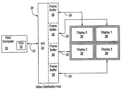
The hub 20 is comprised of two major circuit blocks,
an analog-to-digital (A/D) front end 24, and plus. al frame
buffers 26. The A/D section 24 converts the color data for
each of the RGB colors into a digital representation, and
providers temporary storage for this digital data. There is
one frame buffer per color per associated display device
28, or head: the frame buffers are each comprised of data
gate arrays (to :be discussed subsequently) which enable the
storage of a selected portion of the video data coming from
the VGA 18 in a local memory. The selected portion then is
read out of the memory and is made available to the
respective head 28 through a frame buffer output interface
and associated cable 30.
The hub is an enclosure having approximate dimensions
of seven inches :in width, one inch in height, and nine
inches in length, though other hub embodiments assume other
relative and absolute dimensions. Heat relief is provided
as required. Physical interfaces include an input port for
receiving the RGB video stream over the video cable 22, a
power supply connection for interfacing to a +12V
unregulated (or regulated) power supply (not shown), and
CA 02335530 2000-12-19
WO 99/66489 PCT/US99/13442
-13-
output. ports for each frame buffer 26 enabling
interconnection of the display device cable 30. LAN ports,
such as a BNC connector and RJ45 connector, enabling
intercommunication between plural hubs are also provided in
one embodiment. A serial port is also provided, enabling a
remote host (not necessarily the same host as that which
houses the respective video graphics adapter) to provide
command and control data to the hub, and to return data.
This serial link c:an be used, for instance, to command the
hub to initiate communication over the LAN with other LAN-
connected hubs. In an exemplary embodiment, this serial
port is an RS232 port.
In a preferred embodiment, the A/D section 24 and two
of the frame buffers 26 are disposed on a first. circuit
card within the hub 20. Two further frame buffei:s 26 are
located on a separate circuit card, also within the hub 20.
In addition, :in a further embodiment of the present
invention, up to eight frame buffers are supported within
the hub, all interfacing through a single A/D 24. Physical
dimensions for such a hub 20 would of course be adjusted to
accommodate the additional circuit cards.
The present .invention is discussed at a more detailed
level with respects to Fig. 3. Here, the video display
buffer 32, otherwise known as a large frame buffer, is
illustrated in as:>ociation with the video graphics card 18.
Again, the RGB video data is illustrated as being conveyed
from the video graphics card 18 to the hub 20, and in
particular to the A/D section 24. Further detail on the
A/D section is presented below.
Between the A/D section 24 and the plural frame
buffers 26 is an internal bus 34. As shown, this parallel
bus is 48 bits wide; there are eight bits per pixel per
each of the three colors, or twenty-four bits per pixel,
and it is desired t:a transmit two pixels per clock cycle.
3~~ Over this bus :34 flows all of the digitized video data
which corresponds to the complete contents of the video
display large :Frame buffer 32 as received by the A/D
CA 02335530 2000-12-19
WO 99/66489 PCT/US99/13442
-14-
section 24. It is within the frame buffer 26 logic that
the determination of where to begin storing data and where
to stop is made. By starting and stopping the storage of
video data, each frame buffer section 26 is capable of
providing to the x-espective video head 28 only that portion
12 of the total 'video display buffer 32 which is desired.
In Fig. 3, the frame buffers 26 are each illustrated
as being comprised of a logic section 36 and an SGRAM
(synchronous graphics RAM) 40. Essentially, the logic 36
is responsible for storing in the SGRAM 40 only video data
associated with the video buffer portion 12 desired to be
displayed on the respective display device 28. 'rhe SGRAM
40 provides temporary storage of this data to enable the
timely provision c>f the data to the respective head 28. As
will bE: discussed subsequently, there is logic and SGRAM
associated with each color for each of the display devices.
With respect to Figs. 4 and 11, the A/D section 24 is
described in detail. An analog front end 42 AC couples the
received analog RGB signal from the video cable 22. After
being coupled in, the video signal for each color is
approximately 0.~~ Vpp, from the darkest to lightest
extremes. Therefore, it is necessary for the analog front
end 42 to amplify the video signal for each color, thus
improving the signal to noise ratio (SNR) of the following
A/D converters (ADCs) 50. Suitable video preamps for this
purpose include the National LM 1205 and LM 1283.
Gain control for these amplifiers (one per color) can
be either fixed or variable, depending upon the embodiment.
Most simply, the gain control is fixed by the factory. In
3C a further variant, the gain control is fixed. in the
factory, though t=he user has physical access to a gain
control adjusting means.
In another embodiment, the gain control is variable
and is controlled by a control circuit 44 in the A/D
3c; section 24 having a digital to analog converter (DAC) for
generation of the control signal. An appropriates D/A for
this purpose is i~he Analog Devices AD8403AR10. The gain
CA 02335530 2004-05-18
-15-
control (also referred to as contrast control) is adjusted
jointly for all three amplifiers (i.e. each of RGB). In addi-
tion, there are manual, independent balance adjustments for each
of the colors.
One A/D per color is employed in the embodiment of the
present invention. An alternative embodiment employs pixel
merging due to the compression afforded by this technique.
Pixel interleaving is described in commonly assigned U.S. Patent
No. 5,742,274 entitled "Video Interface System Utilizing Reduced
Frequency Video Signal Processing". In a third embodiment of
the present invention not employing such interleaving, two A/Ds
per color are used for video rates above 75 MHz.
Since the analog input is AC coupled, it is necessary for
the analog front end 42 to also perform DC restore in order to
establish a reference level in the amplified analog signal, for
each of the colors. A back porch clamp is employed for the pur-
pose of clamping the amplified input signal to a known reference
during a clamp interval, and is illustrated in Fig. 12. Other
clamping or DC restore techniques can be employed.
In the preferred embodiment, eight bits per primary color
are digitized. A suitable device for the A/Ds 50 includes the
Philips TDA8714. In an alternative embodiment, six bits are
employed for color representation. The choice hinges upon
desired (or required) color depth.
The eight-bit video data representations per color are
clocked into two banks of pixel bus buffers 54. One pixel's
worth of data is clocked into one bank of buffers 54 on even
pixel clock cycles, while another pixel's worth of data is
clocked into the other bank of buffers 54 on odd pixel clock
cycles. Suitable buffers for this function include 74LVT574SM
chips from Texas Instruments.
Also, in the A/D circuit block 24 is a sync processor 46,
such as a Mitsubishi M52347SP. There are three common video
sync protocols. In the first, each of HSYNC and
CA 02335530 2000-12-19
WO 99/66489 PCT/US99/13442
-16-
VSYNC are provided separately as digital signals between 1
- 5 Vpp. In the second, a composite digital sync signal is
provided on the HSYNC signal line. Lastly, an analog
composite sync signal is extracted from the green analog
signal ("sync on green", or "SOG"), with a negative
polarity for positive video. Inputs to the sync signal
processor 46 therefore include externally received HSYNC
and VSYNC, as well as the green analog input signal. The
sync processor 46 is configured to automatically select a
suitable one of these protocols.
Outputs of t:he sync processor include: HSYNC+ and
VSYNC+, correlating to HSYNC and VSYNC signal timings,
respectively; CLAMP+, used by the analog front end 42 in
timing the DC restore, as previously discussed: and status
bits usable by loc:a.1 processing to indicate what sync type
was input to the sync processor 46.
HSYNC+ is used as an input to a phase fine tune (PFT)
circuit 48. The PFT 48 adjusts where the video signal is
sampled by the ADC'. 50 within a pixel lifetime by employing
an adjustable delay of HSYNC+. The output o:f an RC
charging circuit such as that shown in Fig. 14 is compared,
using for instance an Analog Devices AD9696, with a control
voltage generated by the control circuit 44 in the
generation of H(pft)+. An external adjustment such as an
encoder is provided on the exterior of the hub 20 chassis
to enable manual adjustment of the control voltage, in an
illustrative embodiment. Other encoders exist, such as
those on the attached heads 28. The state o f these
encoders is also reported back to the control circuit 44.
Therefore, the present invention is responsive to
adjustment of PFT at either a central location such as the
hub, or remotely, ouch as at the heads.
Also within the A/D circuit block 24 is a video clock
regenerator circuit 52 including a fully programmable clock
regenerator such as an ICS1522 made by Integrated Circuit
Systems, Inc., a phase locked loop (PLL) .frequency
synthesizer. The clock regenerator is serially programmed
CA 02335530 2000-12-19
WO 99/66489 PCT/US99/13442
-17-
in a preferred embodiment of the present invention by the
control circuit 49 to generate four clock outputs, each at
1/4 the sampled pixel rate and 90 degrees out of phase with
the following output, which collectively comprise a clock
at the sampled pixel rate. Various frequencies are
employed, depending upon the video data rate. For
illustrative purposes, 75 MHz is used herein.
In addition to the clock regenerator/.frequency
synthesizer, the clock regenerator circuit 52 is comprised
of a MOSFET bus switch, such as a Texas In;struments
74CBT3125 quad buy; switch. The purpose of the MC>SFET bus
switch :is to generate two 75/2 MHz clocks, 180 degrees out
of phase with each other, from the four 75/4 MHz staggered
clock signals :From the clock regenerator/frequency
synthesizer.
With respect. to Fig. 15, four switches are provided in
the 74CBT3125 bus switch used in the preferred embodiment.
Each switch is a MOSFET switch having an inverted-input
output-enable associated therewith. The first clock signal
from the clock regenerator is fed to the input of the first
switch, and the second clock signal, 90 degrees. out of
phase (lagging) with the first clock signal, is r_onnected
to the output enable for the first switch. The third and
fourth clock signals are connected to the second switch in
a similar manner. The outputs of the first two switches
are then tied together, providing an output clock with
clean rising edges due to the speed of the switches and
having a period of 75/2 MHz.
Likewise, clock two is connected to the :input of
switch three, and clock three is connected to the output
enable of switch three. Clock four is connected to the
input of switch four, and clock one is connected to the
output enable of switch four. The outputs of switches
three and four are also tied together. The resulting
output is also a 75/2 MHz clock signal, though 18C1 degrees
out of phase with the output from the first two switches.
Each of the '15/2 MHz outputs from the bus switch are
CA 02335530 2000-12-19
WO 99/66489 PCT/CIS99/13442
-18-
used to clock a respective PLL clock driver such as the
CDC536 from Texas :Cnstruments as part of the video clock
regenerator 52. 'This part enables the generation of a
doubled output, a 75 MHz clock also referred to as the
ADCLK or "dot clock", which is used to clock the ADCs 50.
Once again, other- frequencies are employable as required.
In additions the clock driver provides 75/2 MHz clocks
("PCLK/2+" and "PCLK/2-") of like phase with respects to the
clocks from which they are derived. Such clocks are used
to clock the pixel bus buffers 54 latching digital video
data ou.t of the ADCs 50, since data gate arrays in the
frame buffer logic: 36 can't run at speeds such as 75 MHz
(data gate arrays are discussed later).
In the first embodiment of the present invention, the
sampling rate does not exceed 75 MHz, with the limitation
being found in the analog preamplifier of the analog front
end 42 and in the: apeed of the ADCs 50.
The clock rE:generator circuit 52 also enables the
regeneration of HSYNC, in a form referred to as LOCHSYNC,
or local HSYNC, aven without an external HSYNC. Thus, an
on-screen display chip is utilized in a further embodiment
of the present invention for the generation of on-screen
menus. LOCHSYNC is employed by the control circuit 44 in
controlling the output of the frame buffers 26.
The on-screen display chip (not illustrated) is
employed in the A/'D circuit block 24, and specifically, in
conjunction with t=he analog front end 42. Analog output
from this chip i.s mixed into the A/Ds 50. A single user
interface to this chip is provided.
In one embodiment of the present invention, control
over when and for what duration a frame buffer 26 captures
video data resides within the A/D circuit block 29, and in
particular within the video clock regenerator 52 using
gating signals. However, since such signals would only
gate one frame buffer 26, such embodiment is not preferred.
The control circuit 44 provides a VSYNC disable to the
video <:lock regenerator 52 to disable the PLL during
CA 02335530 2000-12-19
WO 99/66489 PCT/US99/13442
-19-
vertical intervals. Otherwise, spikes generated by the PLL
in the vertical interval would cause errors in forward
error correction.
Functions of the control circuit 44 in the A/D circuit
block f4 have previously been alluded to, such as the
generation of the analog preamplifier gain control,
creation of VControl for use in tha PFT 48, generation of
the Vsync disable and serial data signals for use in the
video clock regenerator 52. Structurally, the control
circuit comprises in a preferred embodiment the following
elements.
As discussed, a DAC is required in the generation of
amplifier gain ~~ontrol. Other elements comprising the
control circuit include a serially programmable digital
potentiometer, such as an Analog Devices AD8403AR10, which
enables the gener-ation of A/D circuit-internal control
signals such as; CONTRAST, an adjustment to the video
preamp _Ln the analog front end 42; CLAMP WDTH, used in the
sync signal processor; and the PFT control signal
previously discussed.
Primarily, however, the control circuit is comprised
of a C25 microprocessor with an XC5202 microprocessor gate
array. Principal signals received by the control circuit
44 include clocks from the video clock regenerator 52, and
HSYNC+ and VSYNC+ from the sync processor 46. Clearly, in
the actual implementation, there is a much higher degree of
interconnectivity than that which is alluded to here.
For. the purposes of programming the control circuit
44, a serial PROM and a parallel EEPROM provide data to the
gate array and m_~croprocessor, respectively. ThE~ use of
the parallel EEPROM enables the reprogrammability of the
hub. Further, the microprocessor and associated gate array
are in communication with devices external to the hub 20
via a serial port disposed on one end of the hub 20. A
DART (universal asynchronous receiver/transmitter), such as
a TL16C550A, and a TTL to EIA level translator such as an
MAX211E, enable this serial communication.
CA 02335530 2000-12-19
WO 99/66489 ~ PCT/US99/13442
-20-
The control circuit is also in communication with
devices external t:o the hub 20 through LAN ports, such as
BNC or RJ45 connectors. Standard LAN interfaces are
employed in a preferred embodiment, such as an SMC91C94 LAN
chip, coupled to a DP8392 encoder. Such a LAN interface
enables programmability of the hub 20 as an addressable
port on a LAN shared by devices other than hubs, or as a
port on a LAN dedicated solely to one or more hubs in
communication with a configuring device or devices. In
either case, the hub 20 is a "dumb" device which only
responds when directed to from an intelligent device. The
serial communication can be either lOBase2 or lOBaseT.
Finally, as previously noted, a DDC bus enables
configuration of the hub 20 by the host computer 7.6. This
bus is ~~omprised of two data signals, SDA (serial data) and
SCL (serial clock), +5 VDC, and return. The DDC channel is
normally employed, in the prior art, as a unidirectional
pathway to a repository of peripheral device configuration
informal:ion available to a host. Here, however, the C25
processor reads and writes the DDC memory dynamically with
information pertaining to the configuration of the hub and
the attached heads. The DDC memory, which can be discrete
or part of the ~~ontrol circuit memory, is then read by a
host.
Therefore, the control circuit can be configured, or
reconfigured, via internal replacement of programmed memory
devices, external communication to removable configuring
devices such as via a LAN interface, or by input from the
host computer. :3uch configuration information can include,
explicitly or implicitly, the point (row and pixel) within
the frame at which each displayed segment is to begin.
From the A/D circuit block 24, digital video data is
provided in parallel as eight bits per color per pixel,
with two pixels being provided per clock cycle, for a total
of 48 bits. Other signals which are provided by the A/D
circuit block 24 include: USB signals, which are for future
expansion in the present embodiment and are 'therefore
CA 02335530 2000-12-19
WO 99/66489 PCT/US99/13442
-21-
terminated at a daughter board connector proximate the
frame buffer circuitry; horizontal and vertical sync
signals from the sync signal processor 46; various clock
signals originating in the video clock regenerator 52; a
start of frame signal generated by the control circuit 44
from the horizontal and vertical syncs; and serial control
data also generated by the control circuit 44.
One frame buffer circuit block 26 is illustrated in
Fig. 5 at a first order of detail, bearing in mind that
1c) there are up to four frame buffer circuit blocks 26 in each
hub in a first embodiment, each capable of providing
digital video data to a respective display head 28..
Sixteen parallel bits of video data per color (two
pixels) are received by a respective data gate array 56.
la The data gate array 56 enables the storage of the video
data in the respective SGRAM 40 if the data is part of the
desired portion 12 of the video display buffer in the VGA
18, based upon control received from an associated control
gate array 58. In the preferred embodiment of the present
2c) invention, there is one control gate array 58 per frame
buffer logic c_Lrcuit 36, though in an a7_ternative
embodiment, one control gate array 58 is shared between two
frame buffer logic: circuits 36.
If the video data is desired for display on the
2> associated head 28, the data is stored in the respective,
single--ported SGRAM 40. As required, the data is then
removed from the SGRAM 40 where it passes again through the
data gate array 56 to the PANELLINKTM 60, the latter acting
as an output interface to the associated head 28.
3c) On a more detailed level, Fig. 6 provides an
illustration of a data gate array 56 and an associated
SGRAM 40 for a single color channel. Video data input to
the data gate array 56 for one of the three colors, two
parallel eight-bit pixels, is received on sixteen parallel
35 signal paths at approximately 80 MPixels/sec (or 40
MPixelPairs/sec) within a demux 63 in the data gate array
56. This demux 63 enables the distribution of the input
CA 02335530 2000-12-19
WO 99/66489 PCT/US99/13442
-22-
data into two aixteen bit registers 64, which in turn
provide thirty-two bit parallel data to a 32 bit wide, 16
bit deep write FIFO 66.
How the data is transferred into the registers 64
depends upon the type of head 28 associated with this color
channel as conveyed by the head 28 to the control. circuit
44 (via the DDC backchannel) through the serial port to the
control gate array 58 (on a separate serial bus). For an
active matrix LCD display, all eight bits per pixel are
utilized. As shown :in Figs. 7 and 9, the upper of the two
registers 69 is filled with four four-bit nibbles during
clock cycle zero, representing two eight-bit pixels for
this color. On clock cycle one, two more pixels are loaded
into the lower ~;i:~teen-bit register 64. On the following
clock cycle, clock cycle two, the 32 bits of data
representing four pixels for this color are clocked into
the writ=e FIFO 66 and the upper register 64 is writaen with
the next two pixe7_s. The clock speed into the write FIFO
66 is 20 MHz for active matrix displays in the first
embodiment of the present invention. Other exemplary
embodiments employ other clock speeds.
If the associated head 28 is a passive matrix display,
the lower four b~.ts of each eight bit pixel are dropped and
the upper four bits are clocked into the registers 64 as
indicated in Figs. 8 and 10. On successive clock cycles,
the upper four bits for each pixel are stored in respective
portions of the registers 69, while the lower four bits are
dropped.. On clock cycle four, the data in the registers 64
are clocked out to the write FIFO 66 and the process of
receiving the upper four bits per pixel in the registers 64
begins again. The: clock speed into the write FIFO 66 for
passive matrix displays is 10 MHz.
The output of the write FIFO 66 is connected to a 32
bit data path. Also connected to this data path are the
. respective single-ported SGRAM 40, which is 32 bits wide by
256 kbytes deep, and a read FIFO 68 of the same dimensions
as the write F:LFO 66. A suitable SGRAM 40 for this
CA 02335530 2000-12-19
WO 99/66489 PCT/US99/13442
-23-
application is an IBM038329N06A-10, which operates at 50
MHz. Desired video buffer portion 12 data from t:he write
FIFO 66 is read into the SCRAM 40 under the control of the
control gate array 58.
In a first embodiment of the present invention, data
out of the write FIFO 66 is written to the SCRAM 40 for
eight clock cycles, the 32-bit wide bus is idle for two
clock cycles, data is read out of the SCRAM 40 and into the
read FIFO 68 for eight clock cycles, then the bus goes idle
for another two clock cycles. The desired portion. 12 data
can be any contiguous portion of the video buffer data from
the video graphics adapter 18 in the host computer 16,
limited maximally i.n size by the characteristics of the
associat:ed head 2:8.
When and how much data is stored in the SCRAM 40 is
mandated by the control gate array 58. In a first,
preferred embodiment of the present invention, the control
circuit 44 in the A/D circuit block 24 provides the control
gate array 58 i.n the frame buffer logic block 26 with
horizontal and vertical offsets, relative to the start of
frame notification, via the serial data path between the
two for the commencement of data storage in the SCRAM 40.
These offsets are used to control a video microsequencer
implemented in the control gate array 58 for enabling the
transfer of digit:al video data into the video registers 64,
and subsequently into the write FIFO 66. A memory
controller, also implemented in the control gate array 58,
controls the transfer of data from the write FIFO 66 to the
SCRAM 40, and frc>m the SCRAM 40 to the read FIFO 68.
Finally, a panel microsequencer, again, implemented in the
control gate array 58, controls the output of data from the
read FIFO 68 to Frame Rate Modulation (FRM) :Logic 70
(discussed subsequently).
The benefit of providing these three independent
elements, the video microsequencer, the memory controller,
and the panel sequencer, lies in that the writing of data
can take place at: a different rate than the reading of
CA 02335530 2000-12-19
WO 99/66489 PCT/US99/13442
-24-
data t:he memory controller effectively disconnects the
potentially disparate write and read function rates.
The programming of the video microsequencer with the
offset information is preferred due to the ease of
adjusting the offset values when a respective head is
replaced or when the display characteristics for a head are
changed. How much data to store is calculated by the
control circuit 44 based upon display size, resolution, and
orientation as learned from the respective head 28 via the
DDC backchannel. The frame signal is used for interlaced
video applications, the control gate array 58 using this
signal t:o identify even versus odd frames.
In alternative embodiments, data storage in t:he SGRAM
40 is solely under. the control of the control circuit 44,
the latter sending the equivalent of "on" and "off"' signals
to the control gage array 58. A drawback of such control
lies in the need for separate control lines between the
control circuit 94 and each control gate array 58.
In yet another embodiment, the control circuit 44
provides "on" signals to the control gate array 58, and the
control gate array 58 provides the "off" signal based upon
backchannel inform;~t.ion relating to the associated head 28.
The multiplicity of control signals is once again a
drawback: of this embodiment.
The memory controller tracks the data flowing into and
out of the FIFOs 66, 68 and the SGRAM 40. If the write
FIFO 66 is less than half full, a write to the SGRAM 40
from the write F:LF'O 66 is disabled; if the read FIFO 68 is
more than half full, the SGRAM 40 is prevented from writing
to the read FIFO 68. The bus intermediate the FIFOs 66, 68
and the SGRAM 40 remains idle during the clock cycles which
would otherwise bE: used for writing data from or reading
data to the SGRAM 40.
From the read FIFO 68, data is clocked into a frame
rate modulation logic circuit (FRM) 70 which formats the
32-bit wide data according to whether the associated head
28 is passive or active matrix, and outputs eight--bit wide
CA 02335530 2000-12-19
WO 99/66489 PCT/US99/I3442
-25-
data to the PANELLINKTM 60 associated with that frame buffer
26 (the:re is one PANELLINKTM 60 per frame buffer 26) . For
active matrix displays, the FRM 70 executes an algorithm
which reserializes the input data by taking the four,
eight-bit wide pixels, buffering them, and outputting the
data as sequential eight-bit wide pixel data. ThE: maximum
input rate into the PANELLINKTM from the FRM 70 is up to 65
MHz in t:he present embodiment.
For_ a passive matrix array as the associated head 28,
the FRM 70 executes a conversion algorithm which also
receive s 32 parallel bits, but in the form of eight, four
bit pixels. The algorithm converts the four bit pixels
into on.e-bit pixels using frame rate modulation. This
involve: the use of a look-up table in the FRM 70 and the
frame number which is passed from the A/D control circuit
44 to the control gate array 58 to the FRM 70. The
algorithm effectively averages the color of the same pixel
over time, and compares the possible values for this pixel
against that of surrounding pixels to enable the use of
one-bit per pixel with minimized visual artifacts. The
output of the FRM 70 for an associated passive matrix
display is eight parallel one-bit pixels. Alternatively,
any suitable FRM technique may be employed.
In an alternative embodiment in which the speed of the
SGRAM 40 is sufficiently greater than that currently
available, the data format for an associated passive matrix
display could be four eight-bit pixels in parallel into the
FRM 70, instead c>f the current eight four-bit pixels.
In a passive matrix display, the frame rate is twice
that of the active matrix display. Typical values are 120
Hz frame rate for a passive matrix display versus E>0 Hz for
an active matrix display. The chief advantage of passive
matrix displays is cost; presently, such passive displays
cost roughly one-third the cost of active matrix displays.
An active matrix display may take two pixels per clock
cycle, in order. However, a "dual scan passive" display
provides four one-bit pixels per clock cycle at bath a top
CA 02335530 2000-12-19
WO 99/66489 PCT/ITS99/13442
-26-
and bottom half of a display, Thus the difference in frame
rate.
The PANELLINKTM 60 receives eight bits per pixel per
color, or 24 bits per pixel total, at up to 65 MHz for an
associated active matrix panel head 28, four time s the FRM
70 input clock rate. The PANELLINKTM 60 receives pixel data
for an associated passive matrix display at approximately
20 MHz, the same as the input rate into the FRM 70.
The PANELLIN:KTM 60, such as a Chips & Technologies
65100, formats t=he input data for provision to the
respective head 28. It receives the three eight--bit data
streams from the fRMs 70, one for each color, and using the
HSYNC and VSYNC signals from the A/D control circuit 44 via
the control gate <~rray 58 formats the data for output over
four differential lines at a connector to the respective
head 28.
The PANELLINKTM provides its outputs to the respective
head 28 over the display device cable 30 as four twisted
pairs. This cable 30 also provides 12V power and ground, a
USB backchannel (the latter not being employed in the
present embodiment), and the DDC backchannel to the control
circuit 40. Four of the twisted pairs are for the RGB data
and data clock. One twisted pair is for the DDC
backchannel. Another twisted pair is for the USB. Each of
the USB and DDC backchannels provide individual data and
clock paths, and share 5V, 12V and ground which are also
conveyed in this cable to the respective head 28.
Other elements of the presently disclosed hub 20
include registers which preserve the setup information of
the PANELLINKTM EGO,, data gate array 56, and other elements,
as received from the control circuit 44.
The power requirements for the present hub 20 are
unregulated 12 VDC. This is supplied to DC/DC converters
which generate 5V and 3.3V for use as logic supplies. The
unregulated 12 VDC: is used as an input to an ana:Log power
and control circuit which includes a switching DC/DC
converter 72, as ;shown in Fig. 16. The 12 VDC is applied
CA 02335530 2000-12-19
WO 99/66489 PCT/US99/13442
-27-
to a buck switching regulator drive 74. This drive can
take many forms, such as a switching regulator (e.g. a
Linear Technology LT1376), or a regulator controller. The
output of this drive 74, essentially a 12 Vpp rectangular
wave, :is couplE:d through an inductor 80 to a filter
capacitor (or capacitors) 82 at the output of the inductor
80 in t:he common buck configuration, to supply 5 VDC for
use in the analog .section.
The output of the regulator drive 74 is also employed
to drive a charge pump providing a higher-voltage input to
an auxiliary DC supply circuit, generally designated 84 in
Fig. 16. This circuit 84 includes alternately-conducting
diodes 86, and onE: or more reservoir capacitors 88 coupled
to a rnicropower low dropout regulator (e. g. a Linear
Technology LT1129) 90, effectively providing a regulated,
auxiliary 12 VDC output. Other voltages can be generated,
depending upon system requirements.
In an alternative embodiment of the present invention,
the hub 20 is configured to accept a digital video input.
The data gate array 56 in this embodiment is configured to
properly format the input digital data prior to its
processing by the write FIFO 66, the SGRAM 40, the read
FI FO 68 , the FRM 7 0 , and the PANELLINKTM 60 . Such a hub 2 0
can be configured to accept either analog data input as
previously described or digital data input, or can accept
just digital da::a, eliminating some of the cost: of the
circuitry associated with the analog front end in the A/D
circuit block 24. In an embodiment of the present hub 20
which accepts di.g:ital data directly, buffers such as the
pixel bus buffers 54 are employed to temporarily hold the
digital data prior to processing by the data gate array 56.
In yet further alternative embodiments, the digital
output of the hub is employed as a digital input to one or
more subsequent hubs. The PANELLINKTM interface 60 can also
be replaced with D/A converters. Such an embodiment could
then drive conventional CRTs, or could provide ana:iog input
to one or more subsequent hubs. Additionally, the inputs
CA 02335530 2000-12-19
WO 99/66489 PCT/US99/13442
-28-
and outputs of the hub 20 can be adapted to receive and/or
transmit data in an optical format.
In another embodiment, a configurable hub is provided
which enables the merging of plural, disparate video inputs
into a single pixel bus dataset, and the selective display
of independent portions of that dataset on one or more
display devices which themselves may have disparate input
requirements.
The configurable video hub of Fig. 17 illustrates a
number of integrated circuit cards in mutual communication.
Each of the cards will be discussed in detail
subsequently. The purpose of the hub and cards installed
therein is to accept base image data and/or data for one or
more overlay images via input interface cards. The base
image data, if any, defines the outer bounds of a video
display dataset and is driven onto a pixel bus 114 and
merged with the: overlay image data, if any. At one
extreme, no overlay data exists and the resulting pixel bus
dataset is comprised only of base image data. At the other
extreme, the base image data is completely replaced by
overlay data. In between these extremes, the overlay data
may app>ear as a window of overlay data amidst the base
image. Further ;till, the base image may not be driven
onto the pixel bus at all, such that the overlay data is
driven onto the pixel bus amidst a default video display
value representing the area the base image would otherwise
occupy. In one embodiment, this default value results in
the display of a black pixel within the base image field in
each location where an overlay pixel is not merged.
A system card 110 is installed in each hub for control
purposes, as described below. It is also capable of
receiving input data in the PANELLINKTM format for use as
the base image. Other input cards may also be used, though
the hub can func;t:ion in one embodiment with a system card
and up to five output cards. Fig. 17, in contrast,
illustrates an exemplary configuration employing a system
card 110, three :input cards ( labelled INPUT A, INPUT B, and
CA 02335530 2000-12-19
WO 99/66489 PCT/IrS99/13442
-29-
INPUT C:), and two output cards (labelled OUTPUT A and
OUTPUT B) . Each of the input and output cards may process
more than one data stream, also as discussed below.
Communications between the system, input and output cards
is via various pixel and control buses and discrete signal
paths.
Pixel data is driven onto a pixel bus 114 for
subsequent extraction from the pixel bus 114 by one or more
output interface ~~ards. Each output interface card then
either forwards the entirety of the extracted pixel bus
data to one or more interconnected video display devices,
or forwards a spE:cific portion of the pixel data to an
interconnected display device. In the situation where all
of the pixel buy: data is forwarded to an associated video
display device, i~hat device is provided with a frame buffer
for selectively extracting a portion of the entire pixel
bus dataset fox display.
In a first embodiment of the presently disclosed hub,
there a:re six card slots in a hub chassis, one of which is
occupied by a system card 110, as illustrated in Fig. 18.
The fivE= remaining slots are available for interfacing to a
variety of video input sources and a variety of output
display devices. Other hub embodiments provide a smaller
or larger number of card slots.
The hub also provides a backplane for supporting a CPU
bus 112, a serial control bus 113 from a system card CPU
126, the parallel pixel bus 114, a gate array serial bus
115 and a power supply module (not shown).
The CPU bus 112 is comprised of sixteen data and eight
address lines to and from the system card CPU 126, a
write/read control bit for addressing gate arrays on other
interface cards, and a per slot enable line for each of the
hub slots.
The serial control bus 113 is comprised of a clock
line and a data :Line from the CPU 126, and is used for
writing to and reading from control registers disposed
throughout the hub and for writing to and reading from
CA 02335530 2000-12-19
WO 99/664$9 PCT/US99/13442
-30-
registers associated with frame buffers which may be
disposed in association with display devices external to
the hub.
The pixel bus 114 comprises parallel data lines which
are one pixel (t:wenty-four bits) wide, in addition to
horizontal synchronization (HSYNC), vertical
synchronization (VSYNC), data enable (DE), a pixel clock
line for each hub slot 124, and an overlay control line
(inverse-OVERLAY;. The latter signal is asserted by an
input interface card while it is driving an overlay signal
onto the pixel bus, as described subsequently. The pixel
bus 114 also supports a common pixel clock line 123 driven
by the input interface card providing a base image signal
in the absence of such a base image signal input to the
system card 110.
A first embodiment of the power supply module (not
illustrated) rec:e:ives twelve volts, regulated or
unregulated, and outputs 3.3 volts and 5.0 volts on the
backplane. The CPU 126 is capable of determining the power
requirements of the cards populating the hub, and of
associated display devices which rely upon the hub for
their power. The CPU 126 is also capable of selectively
enabling and disabling certain electronic elements if there
exists insufficient power. For instance, the CPU 126 is
capable of deactivating a frame buffer of a particular
interface card, an element which tends to consume more
power than others, should power requirement~~ exceed
capacity.
Each hub contains a system card 110, such as shown in
Fig. 18. Digital video data in PANELLINKTM format can be
provided as the base image to the system card 110 via a
standard PANELLINKTM interface unit 116. The output of this
interface 116 is pixel data (DATA), HSYNC (H), VSYNC (V),
and a data enable indication (DE), all of which are
buffered in registers 118 under the control of a gate array
120. The PANELLINKTM interface 116, if receiving a
PANELLINKTM video signal, also derives a pixel clock from
CA 02335530 2000-12-19
WO 99/66489 PCT/US99/13442
-31-
the input signal for distribution throughout the hub via
clock distribution logic 122. If the system card 110
PANELLINKTM input :is to be used as the base image, the base
image data will be output to the pixel bus all the time in
the absence of overlay data from one of the other input
interface cards disposed within the hub. Also, the gate
array 120 control. logic on the system card enables the
registers 118 in communication with the PANELLINKTM
interface 116. However, if one or more of the remaining
input interface cards (discussed subsequently) is to drive
overlay data onto the bus, the system card gate array 120,
CPU l2Ei and associated circuitry (collectively comprising
the CONTROL block 111 shown in Fig. 18) have previously
configured those other interface cards with instructions to
output the appropriate block of pixel data onto the pixel
bus 114 and an indication of when, within a frame, to start
this output. Accordingly, the gate array 120, in response
to initiation of the inverse-OVERLAY signal by the overlay
card, disables the system card pixel bus registers 118
while the overlay data is being written to the pixel bus
114 by another input card.
If the system card 110 is not receiving video input
via the PANELLINKTM interface 116, or if it is, but that
video input is not. to be used as the base image, the clock
distribution logic receives a clock 123 from one of the
other input card's installed in the hub. In any case, under
the switch control of the gate array 120, the clock
regeneration logic 122 then provides the pixel clock signal
directly to the gate array 120 of the system card 110 and
to each of the remaining interface cards installed in the
hub via discrete clock lines 124.
If none of the input data is designated as the base
image, or in other words, when only overlay data is to be
provided to the pixel bus 114, the system card gate array
120 (executing software stored in associated memory 128)
selects one of the overlay input signals from one of the
other input cards as a source of pixel clock and sync
CA 02335530 2000-12-19
WO 99/66489 PCT/U'S99/13442
-32-
signals . The choice of which is used for this purpose may
be made based upon pixel clock speed, card slot position,
or some other factor.
In one embodiment of the system card 110, a local area
network (LAN) interface 130 provided in association with
the gate array 1~'.0 of the system card control block 111
provides an interface for a serial control line input, such
as a lOBaseT intei:face. This input is utilized to program
the memory 128 utilized by the gate array 120 and the CPU
126 in configurirng the interface cards of the hub. For
instance, it is through this path that overlay windows are
defined in the hub. The interfaced computer relays to the
hub that a window is to be established at certain screen
coordinates the hub then configures the appropri<~te input
overlay card to begin driving pixel data onto the pixel bus
at the appropriate time such that the window defined by the
computer is provided.
The memory 128 itself is preferably comprised of a
combination of a high-speed flash memory and a RAM scratch
pad area. The, flash memory portion is utilized for
parameter storage, which is the hub configuration and
source characterization information, and a non-volatile
code space is provided for the CPU 126.
The system card control block 111 further comprises a
universal asynchronous receiver/transmitter (UART) 132,
also for the purpose of providing a serial port interface
to the control block 111. In another embodiment, the UART
132 is replaced with a universal serial bus (USB)
interface, which has the capability of providing extra
ports, should the need arise, through the use of an
expander. Either serial interface enables the same type of
overlay control exercised using the LAN interface, as
previously described.
One of the functions which the control block 111
performs is to analyze the received HSYNC and VSYNC from a
video input, received by any of the input interface cards,
for the purpose of identifying the source of t:he video
CA 02335530 2000-12-19
WO 99/66489 PCT/US99/13442
-33-
signal. These signals are provided to the gate array 120
via receivers 134 in communication with the pixel bus 114.
For instance, different video sources use three common
video sync protocols, as previously described. Such source
identification information is useful in determining how
large a frame the source can provide. The source
information is also utilized when the system card gate
array 1~.'0 is programming the new base image card.
Other forms of input interface cards will now be
described. In Fig. 19, an analog input card 140 is
illustrated. A :>tandard video connector 142 is provided to
interface the hub to the source of analog video data, such
as the RGB ouilput: from a standard personal computer
graphic: adapter card. From the connector 1.92, the
received data is buffered by an analog buffer 144 prior to
being passed through an analog-to-digital converter 146,
such as that illustrated in the A/D circuit block 24 of the
video distribution hub, above. As with the system card
110, registers 1.48, under local control, are utilized to
gate the digitizE?d video data onto the pixel bus. The data
will be driven onto the pixel bus 114 when this analog
input card is the base image card, and the base image is
not being overlaid.
The video connector 142 also provides an input to a
sync separation block 150 for the purpose of identifying
the input data format and isolating the HSYNC and VSYNC
from the analog input signal. These sync signals are also
gated to the pixel bus 114 via registers 148 for source
identification by the system card 110.
In additions the video connector output is driven to a
clock regeneration unit 152 for the purpose of extracting a
pixel clock from the received data in the case when the
analog input signal is utilized in the hub as the base
image or default source of reference timing. Whether the
locally recovered pixel clock is provided to the remainder
of the hub interface cards is controlled by a switch 154,
which is in turn controlled by local control logic 156.
CA 02335530 2000-12-19
WO 99/66489 PCT/US99/13442
-34-
In the illustrated embodiment, this local control
logic 156 is implemented in a programmable array logic
(PA1,) unit, which includes one or more register interfaces
control:Led by the CPU bus 112. Other embodiments utilize
specialized registers for this purpose. The control logic
156, programmed by the system card 110 CPU 126 via the CPU
bus 112, performs the simple control functions related to
enabling pixel data output to the pixel bus, outputting the
locally recovered HSYNC, VSYNC and DE onto the pixel bus,
and forwarding the locally recovered pixel clock to the
system card clod: regeneration unit 122.
Another input interface card which can be employed in
the hub is a computer overlay input card 160, as shown in
Fig. 20. In many respects, this card resembles the analog
input card 140 of Fig. 19. At an upper level, boi:h employ
a video connector 142, 162 as an interface to an analog
input signal. E~oth buffer the received video data with a
buffer element 144, 164, and both send the received analog
data through an analog-to-digital converter 146, 166.
However,, the computer overlay input card 160 also Employs a
control gate array 1~8 and associated sync separation block
170 and a clock regeneration unit 172 which, while
analogous to the local control logic 156 and associated
elements of the analog input card 140 from a ma~~roscopic
view, a~~tually provide a more complex level of control over
the received analog video data. This heightened level of
control is necessary in order to control the output of at
least a portion of: the received analog video data onto the
pixel bus as an overlay, as described below.
Another difference between the analog input card 140
and the computer overlay input card 160 lies in the memory
utilized for storing the digitally-converted data prior to
making it available to the pixel bus 114. The memory in
the computer overlay input card 160, in a first embodiment,
is a frame buffer implemented with a form of "ping pong"
memory 174, comprised of two memory banks identified as
MEMORY 0 and MEMORY 1 in Fig. 20, where data coming into
CA 02335530 2000-12-19
WO 99/66489 PCT/US99/13442
-35-
and out of the memory 174 passes through a central data
switch labelled SWITCH. In order to expedite access time,
pixel data being written into the memory 174 goes into one
of the memory banks, while pixel data being read out from
the memory 174 is read from the other one of the memory
banks. The switch changes memory banks at each received or
transmitted frame.
The control lagic for the computer overlay input card
employs a control gate array 168 in a first embodiment
lU which acts as a m:icrosequencer. Thus, the memory switch is
under the control of the gate array, as is the sync
separation block: 1~)0 and the clock regeneration unit 172,
whose outputs are used in order to time the writing to the
memory banks. The control gate array 168 indicates to the
15 sync separation block 170 and the clock regeneration unit
172 what format the received data is in for the purpose of
recovering the syncs, DE arid pixel clock. Thi~~ data is
then made available to the system card, including line
count and frame time, for software source recognition.
20 Received analog video data is selectively buffered in
the memory banks of the memory 174, and is gated to the
pixel bus 114 by registers 175. Both operations are under
the control of the control gate array 168. The gate array
168 is programmed by the system card 110 via the serial
2~~ control. bus to identify a starting point and an offset
within the buffered data for when the overlay data is to
commence. The sE~rial control bus from the system card is
also used to program the computer overlay input. card to
specify the portion of overlay data stored in the frame
30 buffer 174 that is to be output to the pixel bus 119, and
the point within the pixel bus frame data that th.e overlay
data output is to commence. When the overlay commences,
the gate array asserts the inverse-OVERLAY signal. This
signal alerts the input card generating the base image that
3Ep the ovE:rlay card :is writing data to the pixel bus, and that
the base image card should shut off the registers gating
the base image to the pixel bus.
CA 02335530 2000-12-19
WO 99/66489 PCT/US99/13442
-36-
In alternative embodiments applicable to al:L overlay
cards presently disclosed, the instructions from the system
card tc> the input overlay card as to what portian of the
buffered overlay data is to be written onto the pixel bus
at the appropriate time takes a variety of forms. For
instance, overlaid data can be merged into the base image
on the pixel bus 114 on a pixel-by-pixel basis, or
according to various algorithms pre-programmed into the
local control gate array.
As with the analog input card 140, the computer
overlay input card 160 employs registers 176 for the
purpose of either reading in or writing out HSYNC, VSYNC
and DE. The gate array receives the slot copy of the pixel
clock from the aystem card 110, or in the case when this
computer overlay ~_nput card is the base image card, drives
to the system ca rd the pixel clock recovered by 'the clock
regeneration block 172 for redistribution to the other
interface cards. The received pixel clock is reguired in
order i.o synchronize the output of pixel data onto the
pixel bus.
In one embodiment of the presently disclosed hub,
there :is one channel available for receiving an analog
overlay signal c>n the computer overlay input card.
However, other Embodiments, which employ more densely
packed circuits or which employ larger circuit cards, or
both, provide plural channels.
Another input. card which may be utilized in the
presently disclosE:d hub, depending upon the needs of the
hub user, is a broadcast video (BVIDEO) overlay card 180,
as shown in block form in Fig. 21. This card is utilized
to receive broadcast video data, in one of many formats, to
buffer the data in an on-board memory, and to selectively
output the buffered video data onto the pixel bus.
A comparison of Fig. 21 and Fig. 20 reveals that the
BVIDEO overlay card 180 resembles the computer input
overlay card 160 .in many respects. Each has an input
interface specific: to the expected data. Each has a buffer
CA 02335530 2000-12-19
WO 99/66489 PCT/US99/13442
-37-
memory.:for selectively storing the received pixel data, and
for enabling the writing of selected portions of that data
onto the pixel bus. Further, each has control logic for
controlling these :Functions.
Wii~h regard i=o Fig. 21, the BVIDEO overlay card 180
uses a broadcast video decoder 182 appropriate for the
format of the rEac~aived video data, which can be in NTSC,
PAL, or any other video format. This decoder provides the
video data in digital form to a sealer 184 in a first
embodiment. This sealer selectively reduces the digital
pixel dataset, tea a degree specified by a user in view of
memory capacity and speed, and required resolution at the
display device. The output of the sealer in this
embodiment is then fed to the memory 186, which is also a
"ping pang" memory in a preferred embodiment, as described
with respect to the computer overlay input card of F'ig. 20.
In alternative embodiments of the BVIDEO overlay card
of Fig. 21, the sealer 184 is utilized at the output of the
buffer memory 186, in order to reduce the resolution of a
segment of data too be displayed such that a larger overall
picture fits into a smaller overlay window. Thus, the
scaling performed by the sealer 184 will depend upon the
resolution desired in the overlaid window. The sealer is
therefore programmable by the associated control gate array
188, whether the sealer is before the memory 186 or after.
In yet a further embodiment of the present invention, no
sealer is utilized.
In most respects, the function of the control gate
array 188 for the BVIDEO overlay card 180 is the same as
that handled by the control gate array 168 of the computer
input overlay card 160. The control gate array 188 is
responsible for z°eceiving overlay location information and
buffer segment to be displayed information from the system
card 110 via the serial control lines, for receiving the
slot copy of the pixel clock from the system card 110, for
receiving the HYSNC, VSYNC, and DE signals from the system
card via registers 190 which it controls, for controlling
CA 02335530 2000-12-19
WO 99/66489 PCT/US99/13442
-38-
the function of the ping gong memory switch, and for
controlling the registers 192 which gate the pixel data out
of the memory 186 onto the pixel bus 114. In addition, the
control gate array 188 receives HSYNC, VSYNC, DE and the
pixel clock from the broadcast video decoder 182 for
enabling source identification carried out by the system
card 110. When specified by the System Card, the gate
array within the BVIDEO overlay card drives recovered
HSYNC, VSYNC and DE signals onto the Pixel Bus 114 via
registers 191. Note the distinction between this card 180
and the computer input overlay card 160 - there is no
discretE: sync separation block or clock separation unit,
since those functions are implemented in the broadcast
video dE:coder. The video decoder 182 is configured for the
received video data format by the control gate array, via
the serial control buses.
In a preferred embodiment of the presently disclosed
video hub, there are two BVIDEO overlay circuits, such as
that shown in Fif. 21, on a single circuit card. Each such
circuit employs the elements shown in Fig. 21. Alternative
embodiments provide only a single overlay circuit per
circuit card, or more than two such circuits per card,
depending upon card size and circuit density.
Anc>ther interface card employed in the presently
disclosed hub is referred to as a data exchange module 200,
shown in Fig. 22. This module enables a user to provide
all or a part of the pixel bus data to an interconnected
device such as a personal computer or another hub. A first
memory element 202, gated by registers 204 under the
control of a local control gate array 206, provides
temporary storage f:or the desired pixel data prior to being
forwarded off board. The system card 110, and the CPU 126
in particular, is responsible for programming the control
gate array 206 of the data exchange module 200 to specify
the portion of the pixel data which is desired.
The data so extracted can also be provided as an input
to another hub as presently disclosed. The extracted data
CA 02335530 2000-12-19
WO 99/66489 PCT/US99/13442
-39-
would therefore include any and all overlay data found in
the pixel data of the local pixel bus 114. A subsequent
hub, receiving such pixel data as an input, would then be
configurable such that further overlaid windows could be
merged ~.nto the pixel data.
ThE: data out of the data exchange module 200 can also
be used as an input to a display device, if properly
buffered and formatted, such as via a PANELLINKTM interface
or any other suitable interface.
A further feature of the data exchange module 200 is
the ability to receive pixel data from another source, such
as from. a corresponding data exchange module in another
hub. f3uch received data is buffered in a second memory
element 208, from which all or a selected portion of the
received pixel data can be output onto the pixel bus, under
the control of the control gate array 206 as programmed by
the system card 110 and using the inverse-OVERLAY signal
protoco7Ls as discussed above, for instance with respect to
the computer input overlay card 160.
Intermediate' the two memory elements 202, 208 and the
external device in communication with the data exchange
module 200 is a data handling element 210, which is
required in order to transfer data from the synchronous
memory elements 202, 208 to an asynchronous bus in
communication with the external device. The data handling
unit 210 is therefore necessary to reformat the pixel data
into the desired output format, and its implementation is
specified by the equipment to be interfaced to. For
instance, the output of the data handling unit 210 can be
video, digital or Rf in various embodiments.
The actual interface between the data exchange module
200 and an interconnected device in one embodiment is a
LAN/comrnunications (LAN/COMM) circuit 212, having an
associai:ed CPU 214. This interface can be configured for
interfacing the respective hub to a 100BaseT data path for
live video output/input, or to a lOBaseT data path for
sending or receiving "snapshots", or discrete frame samples
CA 02335530 2000-12-19
WO 99/66489 PCT/US99/13442
-40-
of pixel data.
Pixel data captured from the local pixel bus 114 can
also beg routed to the LAN used for configuring the
respective hub. The desired data is transmitted over the
system card CPU bus, which is extended across the hub
backplane. From t:he system card, the data is then routed
via the CPU-assac.iated LAN interface 130 to the control
LAN.
Tie control gate array 206 for the data exchange
module 200 is also responsible for receiving, or
transmitaing, HSYNC, VSYNC, and DE via registers 216. As
with other, previously described gate arrays, t:he gate
array of the data exchange module 200 also sets the
inverse-OVERLAY signal when data which it has received from
an external source is being used as an overlay input to the
pixel bus 114. The definition of the overlay from among
the received data,, the selection of the portion of the
overlay data for output to the pixel bus 114, and the
timing of the output of that selected data, is also under
the control of th~~ gate array 206, as programmed by the
system card via the' serial control buses.
A further form of input interface card which is not
illustrated includes an interface responsive to serial
commands for thf~ generation of graphical images. For
instance, certain operating system overlays such as X-
Windows communicate graphics commands rather than the
images themselves. Thus, this interface generates graphics
data in response t=o the received serial commands. These
graphics data are then buffered in a frame buffer such as
that illustrated with respect to the BVIDEO overlay card.
Having discussed a variety of input interface cards
which can be used i~o configure the presently disclosed hub,
output interface cards will now be reviewed. A first form
of output interface is illustrated in Fig. 23, and is
referred to as a triple PANELLINKTM output card 220. Data
from the pixel bus 114, including pixel data, HSYNC, VSYNC,
and DE, is captured in a temporary storage element 222,
CA 02335530 2000-12-19
WO 99/66489 PCT/US99/13442
-41-
which depending upon the embodiment can be either registers
or a memory buffer. The data stored in the storage element
222 is then available to the three PANELLINKTM interfaces
224a, 224b, 224c.
Each PANELLINKTM interface 224 in the triple PANELLINKTM
output card 220 provides the pixel bus data in PANELLINKTM
format along with the sync, data enable, and clock signals.
This output is provided to an interconnected display
device via a cable which in a first embodiment also
provides power to the display device. Connectors 226
adapted for inter°f.acing to such custom cables are provided.
Each displa~,r device connected to the triple PANELLINKTM
output card 220 has associated therewith a frame buffer for
the purpose of storing only the portion of the ~>ixel bus
data which is des:i.red for display on the display device.
The frame buffer then outputs the desired data for
synchronizatian with a display clock. The data is then
made available for display. The triple PANELLINKTM output
card 220 also prcwides a serial control bus 113 link to
each interconnected display device for the purpose of
programming the display device frame buffer, according to
the input provided to the system card 110 by the external
control system, with the portion of the pixel data which is
to be displayed. l7epending upon the implementation, this
data can be in the format of start and stop signals, or a
starting point with an offset to a stopping ,point, or some
other set of controls which identify to the frame buffer
what portion of t:he pixel bus data, via the PANELLINKTM
interface, is to bES buffered and displayed.
A register 2<?8 is coupled to the CPU bus 112. The
register- 228 is used to control a switch 230 which enables
the coupling of the serial control bus 113 and the gate
array serial bus :115 to the interconnected display device
frame buffers. ,since the runs between the hub and each of
the di:~play devices can be quite long, it would be
impractical to try to drive the serial bus to each frame
buffer all the time. Further, addressing is not provided
CA 02335530 2000-12-19
WO 99/66489 PCT/IJS99/13442
-42-
at each frame buffer, so there would be no way for a
particular frame: buffer to distinguish between control
signals intended for various frame buffers. The switch 230
is thus used for selectively routing the serial bus to the
appropriate remote frame buffer.
In alternative embodiments of the present hub, the
triple PANELLINKTM output card 220 can be provided with one,
two or four or more PANELLINKTM output channels, depending
upon space available on the circuit card and the needs of
the user.
Another embodiment of an output interface card for the
hub is illustrated in Fig. 24. This card is the dual DFP
output card 240, which is similar in some respects to the
triple 1?ANELLINKTM output card 220, with the exception that
the output of thE: presently described card is compliant
with the DFP standard, and the card includes the frame
buffer i=unction an~-board, instead of located at the display
device as with the display device associated with the
triple PANELLINKTM output card 220 of Fig. 23.
In the dual DFP output card 240, pixel data from the
pixel bus 114 is received in temporary storage elements
242, which can be registers or any other suitable memory
element. From there, the buffered data is passed to
respective frame buffers 244 which each employ a ping pong
memory such as that described in conjunction with the
computer overlay input card 160 or the BVIDEO overlay input
card 180. This memory enables the selective writing of
pixel data to the dual memory banks, and the reading of
stored data at the appropriate time, all under the control
of a control gatE~ array 248, programmed by the system card
CPU 126 via the C;Pt:1 bus 112 and the serial control bus 113.
In the illustrated embodiment, the frame buffers 244 are
XGA frame buffers, meaning that each has the capacity to
buffer enough data from among the entire pixel bus dataset
to drive an associated XGA video display device.
The: output of each frame buffer 244 is provided to a
PANELLINKTM interface 246 for the purpose of sending
CA 02335530 2000-12-19
WO 99/66489 PCT/US99/13442
-43-
properly formatted video data to the respective display
device. Alternatively, the output of one channel of such a
dual DFP output card 240 can be used as a PANELLINKTM input
to, for instance, a system card 110 of another hub, or as
an overlay input to another hub. The PANELLINKTM interface
246 output is provided to a standard PANELLINKTM cable
connector 250. In addition, this output interface card 240
provides an extE:nsion of the gate array serial bus 115
which is used, dE:pending upon whether the video display
device is DDC compliant, for the purpose of collecting data
from the display device including technical specifications
such a~~ refresh rate of the attached display device,
backlight operating time, power conditions, and temperature
conditions.
In further embodiments of the presently disclosed hub,
one or three or more video display channels are provided,
depending upon t:ne availability of circuit card space and
the needs of the u;~er.
A further output interface card employable in the hub
of the present invention is a CRT output card 260, as
depicted in Fig. 25. This card also receives pixel bus
data in temporary storage 262 such as registers or memory
buffers. From there, the received pixel data is sent to
memory 264. As i:Llustrated, one embodiment of the memory
269 employs plural ping pong memories and a switch
responding to an associated gate array 268 in order to
improve memory bandwidth. The gate array is programmed by
the system card CPC 126 via the serial control bus 113.
The output c>f the memories 264 passes through a
digital to analog (D/A) converter 266 and is provided to
the associated CRT display device via an appropriate
connector (not shown). In one embodiment in which the CRT
display device provides maintenance or configuration
information via a standard bus such as DDC, the gate array
serial bus 115 from the gate array 120 of the system card
110 is extended to the associated display for gathering
such information.
CA 02335530 2000-12-19
WO 99/66489 PCT/US99/13442
-44- -
One problem with utilizing PANELLINKTM outputs, as with
the triple PANELr..INKTM output card 220 or the dual DFP
output card 240, is that PANELLINKTM cable runs are
typically limited to approximately fifteen feet, whereas it
may be desirable t:o have the hub substantially removed from
the display devices interfaced thereto. One embodiment
therefore employs D/A converters for driving the desired
video data up to and including the entire video space over
distances on the order of 100 feet. Further, the output of
the D/A converter can be passed through a compensation
amplifier in the case of longer cable runs.
In yet another embodiment, the output of the D/A
converter as previously described, or of the compensation
amplifier, is provided at a standardized connector, such as
a Universal Twisted Pair (UTP) connector. Such a connector
can be further utilized to convey other input information,
such as from a keyboard, mouse, or similar serial :interface
device back to an external control system. This connection
can also be utilized to convey serial bus traffic via an
encoder in addition to the pixel data.
Similarly, cable length limitations can be compensated
for on the input side of the hub through, for instance, the
provision of a UTP cable connector at the input to the
analog input card 140. Such a further embodiment of the
analog input card 140 provides, in addition to the UTP
connecto r, an optional compensation filter at the input to
the A/D front end circuitry. This UTP connector would then
be available for receiving other communications, such as
the encoded serial data from a keyboard, mouse or similar
device, or serial. bus traffic via a decoder.
A problem with some analog communications paths lies
in the use of concluctor pairs for discrete portions of the
total ~>ignal, resulting in unsynchronized data at the
receiver. For instance, in one embodiment, an asynchronous
bus is comprised of twisted pair conductors for each of
red, green and b~_ue data paths. These individual data
lines must be rE~-synchronized in order to compensate for
CA 02335530 2000-12-19
WO 99/66489 PCTlUS99/13442
-45-
delays, introduced as a result of unequal conductor lengths.
This can be accomplished by phase fine tuning the
discrete, unsynchz-onized portions of the total data, then
hard clocking thE: data out of the A/D front end of a
variant of the analog input card 140.
A display device which is interfaced to the presently
disclosed hub can have a frame buffer local thereto, or can
be provided with that function through a frame buffer local
to the respective output card. For instance, a display
device to be driven by the triple PANELLINKTM output card
220 of Fig. 23 ha;s its own frame buffer circuit. This is
preferable in one sense in that the frame buffer size can
be customized to the actual display capabilities of the
respective display device. With respect to the dual DFP
output card of F~_g. 24, the frame buffers local to the
output interface card must be made as large as the largest
frame which can be displayed by a display to be connected
thereto.. However, the necessarily large capacity of that
frame buffer may go under-utilized.
A display device 280 (also referred to as a "tile")
having a local frame buffer and adapted for being driven by
one channel of the triple PANELLINKTM output card 220 is
illustrated in F.ig. 26. A PANELLINKTM input interface 282
receives the pixel data from the associated PANELLINKTm
output card 220, and provides it to a frame buffer, such as
the ping pong memory arrangement 284 as shown. As with the
overlay input cards described above, the frame buffer 284
is under the control of a control gate array 286 having a
link to the system card 110 via the extended serial control
bus 113. The control gate array 286 is also in
communication with a microcontrolier 288 local to the
display device 280, which is in communication with the
extended gate array serial bus 115 from the gate array 120
of the system card 110 for the purpose of managing the
power state of the display device, and for tracking and
reporting display run time and temperature to the system
card 11C.
CA 02335530 2000-12-19
WO 99/66489 PCT/US99/13442
-46-
Certain protective features can also be implemented in
some of the output: interface cards. For instance, the
output of the triple PANELLINKTM output card 220 includes
12.0 volts for t:he purpose of powering the associated
display device. A standard PANELLINKTM display element,
which is not expecting power in association with the
PANELLINKTM data, could be damaged if so connected.
Therefore, a further embodiment of the present hub provides
a switching capability for output interface cards, under
the centralized control of the system card 110.
In a further embodiment, an adapter is provided for
receiving a standard PANELLINKTM output and for receiving a
source of power necessary for operation of a display
device. The output of this adapter is then provided over a
single cable, such as the cable connected to the triple
PANELLINKTM output interface card 220, to a display device
which relies upon a power input via the display data cable.
Moctifications and substitutions to the present
invention made ~>y one of ordinary skill in the art is
considered to be w_Lthin the scope of the present invention,
which is not to be limited except by the claims which
follow.