Note: Descriptions are shown in the official language in which they were submitted.
CA 02336333 2000-12-29
WO 00/02255 PCT/US99/14579
TITLE OF THE INVENTION
DIRECT RADIOGRAPHIC IMAGING PANEL HAVING A DIELECTRIC LAYER WITH AN
ADJUSTED TIME CONSTANT
BACKGROUND OF THE INVENTION
1. Field of the invention
This invention relates to radiation sensors in general and more particularly
to a radiation
detection panel comprising a plurality of radiation sensors which include a
dielectric layer
with adjusted resistivity.
2. Description of Related Art
Radiation sensors able to convert incident radiation directly to an electrical
charge indicative of the intensity of the incident radiation are known.
Typically such
sensors comprise a complex structure which includes a bottom and a middle
conductive
electrode separated by a dielectric to form a charge storing capacitor. A
radiation
detection layer, which may be a photoconductive layer, is placed over one of
the
electrodes. Over the photaconductive layer is another dielectric layer and a
top
electrode over the dielectric layer completes the sensors structure. Charge
blocking
layers are often provided between the conductive electrodes and the
photoconductive
layer.
A charging voltage is applied between the top electrode and the bottom
capacitor
plate.
Upon exposure to radiation, a charge proportional to the exposure level
accumulates in the storage capacitor formed by the bottom and middle
electrodes.
Read-out of the stored charge is usually done by addressing the middle
electrode and
CA 02336333 2000-12-29
WO 00/02255 PCT/US99/14579
flowing the capacitor charge to a charge measuring device such as a charge
integrating
amplifier.
A plurality of such sensors may be assembled in an array of rows and columns
to
forti~ a radiation detection panel. By sequentially reading out the charges
accumulated
in the individual sensors an image of the relative exposure of different areas
of the panel
is obtained. This image represents the radiation intensity incident on the
panel after it
has passed through a subject illuminated by the radiation. When the radiation
is X-ray
radiation and the subject is a patient the resulting image is a radiogram,
captured as a
plurality of charges. This radiogram can be displayed on a Cathode ray tube or
other
device for viewing.
The charge stored in the capacitor is read-out using a switch which connects,
upon command, the middle electrode to the input of the charge measuring
device. In
practice such switch is usually an FET transistor created integrally with the
sensor,
having its source electrode connected directly to the middle electrode of the
sensor.
Both the drain electrode and the gate are accessible from outside the sensor.
The drain
is connected to the charge integrator. An electrical signal applied to the
gate switches
the transistor to a conductive state and permits the charge to flow from the
capacitor to
the integrator for detection.
The above described technology is well known in the art and well described in
a
number of publications and issued patents, exemplary of which is United States
Patent
No. 5,319,206 issued June 7, 1994 to Lee et al., and in an article by Denny L.
Lee,
Lawrence K. Cheung and Lothar S. Jeromin, entitled °The Physics of a
new direct digital
X-ray detector" appearing in the Proceedings CAR '95, Springer-Verlag, Berlin,
pp. 83 .
Both the patent and the article are incorporated herein by reference.
The simplified sensor and transistor structure described above, while quite
adequate, is, however, vulnerable to overexposure. The term "exposure" is used
in this
specification to designate the product of the intensity of the incident
radiation times the
time during which the radiation impinges on the sensor.
2
CA 02336333 2000-12-29
WO 00/02255 PCT/US99/14579
When the detector is exposed to radiation, electron-hole-pairs are generated
in
the radiation detection layer which, under the influence of the electric field
produced by
the applied charging voltage, travel toward the top and middle electrodes
respectively. If
such charges are allowed to flow freely, the charge stored in the capacitor
formed
between the middle and bottom electrodes increases continuously. The result of
such
continuous charge increase is an associated voltage increase on the voltage
appearing
on the middle electrode which will eventually result in the catastrophic
failure of the
associated transistor switching element connected to the charge storage
capacitor. The
presence of a dielectric layer between the radiation detection layer and the
top electrode
eliminates this risk by presenting a barrier to the migrating charges, which
begin
accumulating in the interface between the radiation detection layer and the
dielectric
layer. These accumulated charges set up a secondary field opposing the applied
charging field thus inhibiting further charge migration and providing a limit
to the rising
voltage on the middle electrode.
While this is an acceptable solution to the overexposure problem, the
accumulated charges on the dielectric/photoconductor interface will interfere
with
subsequent exposures of the sensor.
In order to eliminate the effect of such residual charges, there is usually
required
an additional step in which the trapped charges are eliminated. This extra
step is not
only time consuming, but, for the reasons discussed later, inhibits the use of
this type of
sensor for continuous, real time imaging, such as in fluoroscopy applications.
It is an object, therefore, of the present invention to provide a sensor, and
an
associated panel comprising a plurality of such sensors, which is protected
from
catastrophic failure due to overexposure during single exposure operation, and
which
still has fast response for use in real time viewing applications.
3
CA 02336333 2000-12-29
WO 00/02255 PCT/US99/14579
SUMMARY OF THE INVENTION
The aforementioned objectives are achieved by a radiation sensor according to
this invention which comprises:
a) a charge storage capacitor;
b) a radiation sensitive layer over said charge storage capacitor;
c) a dielectric layer over said radiation sensitive layer said dielectric
layer having a
time constant i = px~ selected between 0.05 and 20 seconds, wherein p is the
resistivity, x is the dielectric constant of the dielectric layer, and eo is
the
permitivity of free space; and
d) a fop conductive layer over said dielectric layer.
The invention further comprises a method for forming a radiation detection
sensor of the type comprising:
a) a charge storage capacitor;
b) a radiation sensitive layer over said charge storage capacitor;
c) a dielectric layer over said radiation sensitive layer; and
d) a top conductive layer over said dielectric layer.
the method comprising adjusting the resistivity p of the dielectric layer such
that a time
constant i = px~ is set between 0.05 and 20 seconds, x being the dielectric
constant of
the dielectric layer.
The dielectric layer may be a linear segmented polyurethane in which the
resistivity p has been so adjusted.
Finally, the invention also includes a radiation detection panel comprising a
plurality of radiation sensors, each of said sensors including:
a) a charge storage capacitor;
4
CA 02336333 2000-12-29
WO 00/02255 PCT/US99/14579
b) a radiation sensitive layer over said charge storage capacitor;
c) a dielectric layer over said radiation sensitive layer said dielectric
layer having a
time constant ~ = px~ selected between 0.05 and 20 seconds, wherein p is the
resistivity and x is the dielectric constant of the dielectric layer; and
d) a top conductive layer over said dielectric layer.
Preferably, i is around 1 second.
BRIEF DESCRIPTION OF THE DRAWINGS
The invention can be more fully understood from the following description
thereof
in connection with the accompanying drawings described as follows.
Figure 1 is a representation of a radiation sensor in accordance with the
present
invention.
Figure 2 shows a panel comprising a plurality of sensors of the type shown in
figure 1.
Figure 3 shows a simplified electrical equivalent circuit of the sensor of
this
invention.
DESCRIPTION OF THE PREFERRED EMBODIMENTS)
Throughout the following detailed description, similar reference characters
refer
to similar elements in all figures of the drawings.
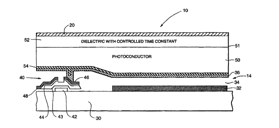
Referring now to figure 1, there is shown in a schematic elevation the
internal
structure of a sensor 10 according to this invention. The sensor is built on a
substrate
30 which may be glass, ceramic, or other suitable insulating material which
provides
enough mechanical strength to support the layers and circuitry comprising the
sensor.
5
CA 02336333 2000-12-29
WO 00/02255 PCT/US99/14579
Also shown are two conductive elements, placed adjacent each other to form a
first or bottom conductive microplate 32, and a second conductive microplate
36. A
dielectric layer 34 is placed between the two microplates to form charge
accumulating
capacitor 14. The conductive elements may be thin layers of a conductive
material such
as indium-tin-oxide, or a thin layer between 50A and 100A of metal.
An FET transistor 40 is also built on substrate 30. Such transistor preferably
comprises a gate electrode 42, a semiconductor 43 which is typically Si, a
contact layer
44,typically an +Si layer, a source electrode 46 and a drain electrode 48. The
source
electrode 46 is connected to the second conductive microplate 36 and the drain
electrode 48 is connected to a conductor leading to a contact for connecting
the FET 40
to a charge detector. The technology for making arrays of FET transistors
connected to
arrays of microplates is well known. (United States patent 5,641,974 issued to
den Boer
et al, discloses in detail the structure and process of making such a
transistor.)
A radiation detection layer which is typically a photoconductive layer 50, and
which preferably exhibits very high dark resistivity overlays the previously
deposited
layers. in radiography, particularly in medical applications, the incident
radiation is X-ray
radiation, and the radiation detection layer is an X-ray photoconductor. The
photoconductive layer may comprise amorphous selenium, lead iodide, lead
oxide,
thallium bromide, cadmium telluride, cadmium sulfide, mercuric iodide or any
other such
material. It may comprise organic materials such as polymers which may be
loaded with
X-ray absorbing compounds which exhibit photoconductivity when the captured
radiation
is X-ray radiation.
In a preferred embodiment, this layer is a continuous amorphous selenium layer
300 to 500 micrometers thick.
A dielectric layer 52 is placed over the photoconductive layer and a
conductive
top electrode 20 is placed over the dielectric layer. Top electrode 20 is
preferably a
layer of indium-tin-oxide; other conductive material such as chromium,
aluminum, etc.
may be used. The top electrode should be selected so that it is substantially
transparent
6
CA 02336333 2000-12-29
WO 00/02255 PCT/US99/14579
to the radiation one wishes to detect. When such radiation is X-ray radiation
the top
electrode is preferably a conductive layer which is highly penetrable by such
radiation.
A thin layer 54, which may be either a unidirectional charge blocking layer
permitting passage of one type of charge and not another, i.e. either negative
charges or
positive, between the second microplate and the photoconductor, or an
insulating layer
which permits no charge flow between the microplate and the photoconductor, is
placed
between the second microplate and the photoconductive layer. Such
unidirectional
charge blocking layers are well known in the art, and are typically, a non-
conductive
oxide created on the microplate surface facing the photoconductor. Co-pending
application serial number 08/987,485 assigned to assignee of the present
invention the
specification of which is hereby incorporated herein by reference, teaches the
use of an
insulating layer rather than a unidirectional blocking layer.
The technology for creating the sensors is preferably vacuum deposition of
alternating layers of conductive, dielectric and insulating materials, and is
well known in
the art. See for instance "Modular Series on Solid State Devices" Volume 5 of
Introduction to Microelectronics Fabrication by R. C. Jaeger, published by
Addison-
Wesley in 1988.
Not illustrated is a programmable power supply for applying a charging voltage
to
the sensor. The power supply is connected to the top electrode 20 and the
bottom
microplate 32 of the storage capacitor.
Referring now to Figure 2, a plurality of sensors 10 may be arrayed on a
supporting structure 12 to provide an imaging panel capable of capturing
radiation
produced images. Such a panel may be made as a single unit or may be a
composite of
a plurality of smaller panels to achieve a desired size. US Patent Number
5,381,014
issued to Lee et al. on October 8, 1996 discloses a technique for making
larger panels
using smaller units.
7
CA 02336333 2000-12-29
WO 00/02255 PCT/US99/14579
As illustrated in Figure 3, the multilayer structure comprising the detector
forms a
number of capacitors all connected in series. In the case where the detector
includes an
insulating layer, there are four primary capacitors connected. in series, Cd,
Cse, Cin and
Cst. Cd is the capacitor formed by the top electrode 20 and the radiation
detection layer
top surface 51 and includes the dielectric layer 52 separating the top
electrode from the
radiation detection layer. Cse is the capacitor formed by the top surface 51
of the
radiation detection layer 50, and the insulating layer 54; Cin is the
capacitor formed by
the interface between radiation detection layer 50 and insulating layer 54;
Cst is the
storage capacitor formed by the middle and bottom microplates 36 and 32
respectively.
As disclosed in the aforementioned article by Lee et al. the capacitor values
are
optimized such that a 10 Vlmicron field is initially applied across the
radiation detection
layer.
Figure 3 shows an electrical equivalent of a sensor, in which the capacitors
Cd,
Cse, Cin and Cst are represented each as a pure capacitor Cd', Cse', Cin' and
Cst' each
connected in parallel with a resistance Rd, Rse, Rin and Rst. For purposes of
this
invention we are interested primarily in capacitor Cd.
Capacitor Cd is represented by an equivalent circuit of a capacitor in
parallel with
a resistor, and has associated with it a time constant i.
(1 ) i = RdCd'.
Where:
(a) Rd = p L/A and p represents the resistivity of the dielectric layer 52 in
the
capacitor; "A" represents the area of the second electrode, and "L" is the
dielectric layer
thickness;
and
8
CA 02336333 2000-12-29
WO 00/02255 PCT/US99/14579
(b) Cd' = xsoAIL and x is the dielectric constant of the material, so = 8.85 x
10'"
FaradsICM being the permitivity of free space. (x = 1 for vacuum).
By substitution of (a) and (b) in (1 ), is seen that:
(2) i = px~.
Therefore, the time constant associated with the dielectric layer is dependent
on
the resistivity p of the dielectric material, and that this time constant can
be adjusted by
varying the resistivity of the dielectric.
In operation, upon exposure to radiation, electron-hole pairs are generated in
the
radiation detection layer. When the charging voltage applied to the top
electrode is
positive, electrons drift toward the photoconductor/dielectric interface and
are collected
there, establishing a reverse field in the photoconductor. This reverse field
opposes the
applied field and eventually grows to the point where further charge migration
is stopped.
The charges trapped in the interface between the dielectric and radiation
detecting layers are not permanently trapped there, but eventually dissipate,
flowing
through the RdCd' circuit at a rate determined by the circuit time constant ~.
By changing the resistivity p of the dielectric material, i may be adjusted
and
consequently the time for the charges accumulated on the interface between the
radiation detector and the dielectric to dissipate, can also be adjusted.
As stated earlier, a plurality of radiation detection sensors arrayed on a
support
are used to create a panel to capture an image. Each of the detectors forms a
PIXEL,
or picture element. The panel is first charged by applying a charging voltage
between
the top electrode and the bottom microplates. It is then exposed to radiation
which
carries image information as a modulated intensity. The radiation impinges on
the panel
for a preset duration, and charges proportional to the radiation intensity are
generated
and stored in the storage capacitors. Appropriate signal processing,
(preferably of the
type disclosed in United States Patent Number 5,648,660 issued to Lee et al.)
is used to
9
CA 02336333 2000-12-29
WO 00/02255 PCT/US99/14579
recover the accumulated charges in all of the storage capacitors in the
detectors in the
panel and to reconstruct a visible image.
In medical radiology there are two vastly different applications and
associated
modes of operating an imaging panel for capturing X-ray generated images.
These are
what would be termed (a) single shot imaging to produce still pictures, and
(b) real time
continuous exposure imaging for real time continuous image observation.
The first kind of imaging is generally referred to as radiography, and
involves the
taking of single exposure still pictures known as radiograms. Exposures are
short,
typically a few milliseconds, often as few as 0.002 sec. and the intensity of
the radiation
is high.
The second method requires a continuing image capture and display, usually in
real time, generally known as fluoroscopy. in this instance the radiation
exposure is
relatively long and the radiation levels low. Exposures of a few minutes are
common,
and the display consists of the real time display of a plurality of
sequentially obtained
images from the panel. Images may be displayed as rapidly as 30 images per
second to
create the visual impression of motion. In such applications the individual
charge
storage capacitors are read out and discharged as frequently as every 0.020 to
0.100
sec.
As mentioned before, in the case of radiograms, because the capacitors are not
discharged until the exposure is over, it is possible that high exposure
levels will raise
the voltage in the middle electrode to a point where the switching element can
be
damaged. Thus it is desirable to encourage charge build up at the interface of
the
photoconductor and dielectric which above produces a counter biasing field and
thus
limits the charge accumulation in the storage capacitor preventing excessive
voltages
from developing and damaging the switching element. Therefore in a panel
useful for
still picture capture, the dielectric layer desirably has a long time constant
i associated
with it.
CA 02336333 2000-12-29
WO 00/02255 PCT/US99/14579
On the other hand, in fluoroscopic applications the radiation intensity is low
and
the storage capacitors are repeatedly discharged during readout. This readout
repeats
every few milliseconds preventing excessive charge accumulation and resulting
switching element damage.
In both applications, it is desirable to obtain an image free of artifacts.
This
requirement means that before a subsequent imaging exposure occurs, any
biasing field
created by the charges trapped in the interface between the photoconductor and
the
dielectric must be either non existent, or at least substantially uniform and
constant over
the full area of the panel.
This, in turn, also means that between exposures, the charge in the interface
between the photoconductor and the dielectric layers must either dissipate
completely,
or, more realistically, rise rapidly to a uniform level and remain
substantially constant
thereafter.
For a panel intended to be used in radiographic applications where single shot
images are obtained every few minutes or so, a dielectric with a time constant
of the
order of seconds and possibly as long as 20 seconds is used, to provide the
needed
overexposure protection. Given sufficient time between exposures, the trapped
charges
will dissipate. Given sufficient time between exposures, one can also use
other methods
to assure the dissipation of charges and elimination of prior exposure
artifacts, such as
flooding the panel with light, as disclosed in US Patent Number 5,563,421
issued to Lee
et al. on October 8, 1996.
For a panel useful for fluoroscopic applications time constants as low as a
few
milliseconds are desirable to assure almost complete dissipation of the
accumulated
charges at the interface between readouts. Time constants of 50 milliseconds
or
shorter, may thus be called for.
tt is now possible to produce a dual purpose panel which is useful in both
types
of medical radiography, by adjusting the dielectric material time constant to
about one
second. Such time constant permits the charges trapped in the interface to
dissipate
11
CA 02336333 2000-12-29
WO 00/02255 PCT/US99/14579
rapidly during long, fluoroscopic type imaging, yet it is long enough relative
to the short,
radiographic exposures used in single shot imaging to provide the needed
charge build-
up which prevents damage to the transistor due to voltage build-up in the
charge storage
capacitor.
A dielectric material which is useful for use in a dielectric layer according
to this
invention is linear segmented polyurethane modified by polyethylene glycol as
disclosed
in the article by Allan W. McLennaghan, Alan Hooper and Richard A. Pethrick
entitled
°LINEAR SEGMENTED POLYURETHANE ELECTROLYTES - II. CONDUCTIVITY AND
RELATED PROPERTIES" published in 1989 in Eur. Polym. J. vol 25 pp 1297-1302 by
Pergamon Press plc.
Example:
A panel useful for both radiographic and fluoroscopic examinations, comprising
an array of a plurality of detectors was constructed by depositing an array of
a plurality
of first microplates on a glass substrate and by building a TFT switching
transistor in a
space adjacent each of the microplates. Connecting leads, as needed, were
placed
between the microplates connecting the drain and gates of the TFT to
connection points
along the panel sides. Additional leads were placed to provide electrical
access to the
first microplates. A dielectric layer was placed over the plurality of first
microplates, leads
and TFTs, and a second plurality of microplates was deposited thereover to
produce a
TFT module. A passivation layer was created over the mo~dle micropfate to act
as a
unidirectional charge blocking layer and p~sverrt dieiec~eiecftical contact
between the
microplate and the photoconductive layer to be coated thereon. Finally the TFT
source
electrode was connected to the middle microplate.
In practice, the TFT modules are fabricated using technology for
microfabrication
of the transistors and capacitors which is well known in the art. See, for
example, the
aforementioned United States Patent 5, 641,974 and the references referred to
therein.
12
CA 02336333 2000-12-29
WO 00/02255 PCT/US99/14579
A radiation detection layer of Selenium photoconductor was next applied to the
TFT module using conventional vacuum deposition techniques.
Apparatus and techniques for vacuum deposition are well known to those skilled
in the art. Vacuum deposition techniques are described, for example, in the
Handbook
of Deposition Technologies for Films and Coatings, 2nd. Ed., R. F. Bunshah,
Ed., Noyes
Publications, Park Ridge, NJ, 1994. Physical vacuum deposition of selenium is
described, for example, in Bixby, U.S. Pat. No. 2,753,278.
Over the Selenium photoconductor was next coated a dielectric layer using
blade
coating, dip coating, or spin coating. The dielectric material was linear
polyurethane
whose resistivity was adjusted by incorporating polyethylene glycol to achieve
p = 3.76 x
10'2 Ohm-cm. With x = 3 and go = 8.85 x 10-'° F/cm, the resulting time
constant is about
1 second.
The dielectric layer was coated over the selenium layer to a thickness of 40
microns. A top conductive electrode was placed over the dielectric layer by
depositing a
thin layer of metal over the dielectric to complete the panel.
Those skilled in the art having the benefit of the teachings of the present
invention as hereinabove set forth, can effect numerous modifications thereto.
These
modifications are to be construed as being encompassed within the scope of the
present
invention as set forth in the appended claims.
13