Note: Descriptions are shown in the official language in which they were submitted.
CA 02336531 2001-O1-03
WO 00/03252 ~ PCT/DK99/00391
MULTI-POINT PROBE
Field of the invention
The present invention generally relates to the technique of testing electric
properties on a specific location of a test sample and in particular the
technique of
probing and analysing semiconductor integrated circuits for example of LSI and
VLSI complexity.
Description of the related art
The most commonly used technique of testing the electric properties of a test
sample involves the generation of resistivity or carrier concentration
profiles of the
surface of a processed semiconductor wafer by the utilisation of a four-point
probe
as described in published international patent application WO 94/11745.
Furthermore, see for example S.M. Sze, Semiconductor devices - Physics and
Technology, Wiley New York (1985).
As shown generally in figure 1, the conventional four-point probe technique
typically
has the points positioned in an in-line configuration. By applying a current
to the two
peripheral points as shown in detail in figure 2, a voltage can be measured
between
the two inner points of the four point probe. Thus the electric resistivity of
the test
sample can be determined through the equation
p = c ~ (VIl),
wherein V is voltage measured between inner points, wherein I is current
applied to
the peripheral points and, wherein c is a geometry factor depending on the
surface
contact separation d and the dimensions of the test sample. Several schemes
for
calculating the correction factors have been developed, see F.M. Smits,
Measurement of Sheet Resisfivities wifh the Four-Point Probe, Bell System
Technical J. 37, 711 (1958), EP 0 299 875 B1, and J. Shi and Y. Sun, New
method
for calculation of the correction facfors for the measurement of sheet
resistivity of a
CA 02336531 2001-O1-03
WO 00/03252 2 PCT/DK99/00391
square sample with a square four-point probe, Rev. Sci. Instrum. 68 1814
{1997).
The four point probe generally consists of four tungsten or solid tungsten
carbide
tips positioned into contact with a test sample, being for example a
semiconductor
wafer. An external positioning system places the four-point probe into
physical
contact with the semiconductor wafer by moving the four-point probe in a
perpendicular motion relative to the wafer surface. Pressure perpendicular to
the
wafer surface has to be applied to the four point probe, in order to ensure
that all
four points obtain physical contact with for example an uneven wafer surface.
Hence the pressure from the tips on the surface varies between the tips. The
tips
are separated by a distance d, shown in figure 1, typically in the order of
0.5 mm.
An alternative to the above described four-point probe is the SR (Spreading
Resistance) probe, described in US Patent No. 5,347,226 and hereby
incorporated
in this description by reference. The SR probe consists of two probe tips
situated on
one cantilever arm. The SR probe is brought into physical contact with wafer
surface by an external positioning system, while monitoring the applied
pressure
such as to accurately control the physical contact to the uneven surface of a
semiconductor wafer. However, since the tips are situated on the same
cantilever
beam the pressure monitored while monitoring the maximum pressure may possibly
leave one tip with an inferior physical contact.
Additionally, reference is made to US Patent No. 5,475,318, US Patent No.
5,540,958, US Patent No. 5,557,214, European patent application EP 0 466 274
and European patent application having application number EP 98610023.8,
national German patent application DE 196 48 475 and national Japanese patent
applications JP 07199219, JP 01147374 and JP H8-15318, which describe the
general technical field relating to methods for measuring resistance and to
production of measurement probes. The US patents are hereby incorporated in
this
description by reference. Furthermore, reference is made to Soonil Hong et
al's
article regarding design and fabrication of a monolithic high-density probe
card for
high-frequency on-wafer testing published in IEEE 1989, pg. 289-292, 7t"
issue,
Changyeol Lee et al's article regarding high-density silicon microprobe arrays
for
CA 02336531 2001-O1-03
WO 00/03252 3 PCT/DK99/00391
LCD pixel inspection published in IEEE 1996, pg. 429-434, 6~" issue, T. Fujii
et al's
article regarding micropafitem measurement with an atomic force microscope
published in Journal of Vacuum Science & Technology B (Microelectronics
Processing and Phenomena) 1991 9~" issue, pg. 666, H.W.P. Koops et al's
article
regarding Constructive three-dimensional lithography with electron beam
induced
deposition for quantum effect devices published in Journal of Vacuum Science &
Technology B {Microelectronics Processing and Phenomena) 1993 11 t" issue, pg.
2386, H.W. Koops et al's article regarding conductive dots, wires, and
supertips for
field electron emitters produced by deposition on samples having increased
temperature published in Journal of Vacuum Science & Technology B
(Microelectronics Processing and Phenomena) 1996 14'" issue, pg. 6, and Q. Niu
et
al's article regarding double tip scanning tunnelling microscope for surface
analysis
published in Physics Rev. B 1995 51g~ issue pg. 5502.
Furthermore, apart from the above described limitations as to establishing
contact
with the surface of the test sample to be tested the prior art probes possess
limitations as to miniaturisation of the testing technique as the probes
hitherto
known limit the maximum spacing between any two tips to a dimension in the
order
of 0.5 mm due to the production technique involving mechanical positioning and
arresting of the individual testing pins or testing tips, in particular as far
as the four-
point probes are concerned, and as far as the SR-probes are concerned exhibit
extreme complexity as far as the overall structure is concerned and also
certain
drawbacks as far as the utilisation of the SR-probe due to the overall
structure of
the SR-probe.
It appears that no technique is currently available for obtaining the electric
properties of individual devices on semiconductor wafers, without possible
destruction of device junctions. Thus, there is a need for a device, which can
perform high-resolution electric property measurements on individual devices,
further minimising the possibility of destruction of semiconductor wafer
surfaces.
An object of the present invention is to provide a novel testing probe
allowing the
testing of electronic circuits of a smaller dimension as compared to the prior
art
CA 02336531 2001-O1-03
WO 00/03252 4 PCT/DK99/00391
testing technique and in particular of providing a testing probe allowing a
spacing
between testing pins less than 0.5 mm such as in the order of 100 nm e.g. 1 nm
-1
pm or even smaller spacing.
A particular advantage of the present invention is related to the fact that
the novel
testing technique involving a novel multi-point probe allows the probe to be
utilised
for establishing a reliable contact between any testing pin or testing tip and
a
specific location of the test sample, as the testing probe according to the
present
invention includes individually bendable or flexible probe arms.
A particular feature of the present invention relates to the fact that the
testing probe
according to the present invention may be produced in a process compatible
with
the production of electronic circuits, allowing measurement electronics to be
integrated on the testing probe, and allowing for tests to be performed on any
device fabricated by any appropriate circuit technology involving planar
technique,
CMOS technique, thick-film technique or thin-film technique and also LSI and
VLSI
production techniques.
The above object, the above advantage and the above feature together with
numerous other objects, advantages and features which will be evident from the
below detailed description of a preferred embodiment of the present invention
is
according to a first aspect of the present invention obtained by a multi-point
probe
for testing electric properties on a specific location of a test sample,
comprising:
(a) a supporting body;
(b) a first multitude of conductive probe arms positioned in co-planar
relationship with surface of said supporting body, and freely extending
from said supporting body, giving individually flexible motion of said first
multitude of conductive probe arms; and
(c) said conducting probe arms originating from a process of producing said
multi-point probe including producing said conductive probe arms on
supporting wafer body in facial contact with said supporting wafer body
and removal of a part of said wafer body providing said supporting body
and providing said conductive probe arms freely extending from said
CA 02336531 2001-O1-03
WO 00/03252 5 PCT/DK99/00391
supporting body.
According to the basic realisation of the present invention, the multi-point
probe
according to the first aspect of the present invention is implemented in
accordance
with the technique of producing electronic circuits, in particular involving
planar
techniques as the probe is produced from a supporting body, originating from a
.
wafer body on which a first multitude of conductive probe arms are produced
involving deposition, accomplished by any technique known in the art, such as
chemical vapour deposition (CVD), plasma enhanced CVD (PECVD), electron
cyclotron resonance (ECR) or sputtering, etching or any other production
technique,
for example high resolution lithographic methods such as electron-beam
lithography, atomic force microscopy (AFM) lithography or laser lithography,
whereupon a part of the original supporting body is removed through mechanical
grinding or etching producing the freely extending conducting probe arms
characteristic to the present invention constituting the test pins of mufti-
point probes
according to the first aspect of the present invention.
The above part, which is removed from the original wafer body, producing the
body
supporting the conductive probe arms may constitute a minor part or a major
part of
the original wafer body and, the supporting body may according to alternative
embodiments of the multi-point probe according to the present invention
dimensionally constitute a minor part or a major part as compared to the
freely
extending part of the conductive probe arms.
The conductive probe arms characteristic to the multi-point probe according to
the
first aspect of the present invention according to the basic realisation of
the present
invention allow the contacting of the multi-point probe in an angular
positioning of
the conductive probe arms in relation to the surface of the test sample to be
tested
as distinct from the above described four-point probe, which is moved
perpendicularly in relation to the surface of the test sample. The angular
orientation
of the conductive probe arms of the multi-point probe allows the flexible and
elastically bendable conductive probe arms to contact any specific and
intentional
location of the test sample and establish a reliable electrical contact with
the
CA 02336531 2001-O1-03
WO 00/03252 6 PCT/DK99/00391
location in question.
The technique characteristic to the present invention of establishing the
contact
between the multi-point probe and the test locations of the test sample by
utilising
an angular positioning of the conductive probe arms in relation to the test
sample
for contacting in a bending or flexing of the conducting probe arms prevents
the
probe arms from mechanically destroying or deteriorating the test sample to be
tested, which may be of crucial importance in specific applications such as
LSI and
VLSI circuitry.
As distinct from the prior art four-point probe arm, the multi-point probe
according to
the present invention including a first multitude of conductive probe arms may
be
configured in any appropriate configuration due to the utilisation of the
production
technique, allowing the conducting probe arms to be orientated in any mutual
orientation in relation to one another and further in relation to the
supporting body
for complying with specific requirements such as a specific test sample to be
tested.
In this context, the particular feature of the present invention, namely the
possibility
of utilising a production technique compatible with the techniques used for
producing electronic circuits, allows the multi-point probe to be readily
configured in
accordance with specific requirements through the utilisation of existing
CADICAM
techniques for micro-systems. However, according to the presently preferred
embodiment of the multi-point probe according to the first aspect of the
present
invention, the first multitude of conductive probe arms are unidirectional
constituting
a multitude of parallel free extensions of the supporting body.
The possibility discussed above, of configuring the multi-point probe
according to
the first aspect of the present invention in accordance with specific
requirements
and, in particular, specific configurations or geometry of the electronic
circuit to be
tested constituting the test sample allows the conductive probe arms to be
positioned on one surface of the supporting body or, alternatively, in
accordance
with an alternative embodiment on two opposing surfaces of the supporting body
or
even on non-opposing surfaces of the supporting body e.g. on neighbouring
CA 02336531 2001-O1-03
WO 00/03252 ~ PCT/DK99/00391
surfaces of a cubic supporting body.
The first multitude of conductive probe arms on one surface of the multi-point
probe
according to the first aspect of the present invention consists of a multiple
of 2,
ranging from at least 2 conductive probe arms to 64 conductive probe arms,
having
four conductive probe arms positioned on one surface as the presently
preferred
embodiment. Application of a test signal to the surface of the test sample
between
the two peripherally positioned conductive probe arms provides a resultant
test
signal between the two inner conductive probe arms, including information of
the
electric properties of the test sample.
The first multitude of conductive probe arms of the multi-point probe
according to
the first aspect of the present invention have a rectangular cross section,
with the
dimensions defined as: width being parallel to the plane of the surface of the
supporting body of the multi-point probe, depth being perpendicular to the
plane of
the surface of the supporting body of the multi-point probe and, length being
the
length of the conductive probe arms extending freely from the supporting body
of
the multi-point probe. The dimension ratios of the first multitude of
conductive probe
arms comprises ratios such as: length to width within the range 500:1 to 5:1,
including ratios 50:1 and 10:1, having the ratio of 10:1 as the presently
preferred
embodiment, width to depth ratio within the range of 20:1 to 2:1, having the
ratio of
10:1 as the presently preferred embodiment. The length of the first multitude
of
probe arms is in the range of 20pm to 2mm, having a length of 200wm as the
presently preferred embodiment. The separation of distal end-points of the
conductive probe arms ranges from 1 ~m to 1 mm, having 20p,m, 40p.m and 60wm
as
the presently preferred embodiments. However, as previously described the
dimensions of the multi-point probe according to the first aspect of the
present
invention varies as a function of the current state of the art in production
technology
and are therefore not a limitation to the present invention.
The distal ends of the first multitude of conductive probe arms comprise a
variety of
optional shapes in continuation of the end of the length opposing the
supporting
body of the multi-point probe according to the first aspect of the present
invention.
CA 02336531 2001-O1-03
WO 00/03252 g PCT/DK99/00391
The continuation of the length of the freely extending conductive probe arms
include shapes as pointed distal end-points, tapered distal end-points or
enlarged
circular, elliptic or orthogonal squared distal ends or combinations thereof.
The
elaboration of the distal end-points of the first multitude of the conductive
probe
arms allows for optimisation of measurements of electric properties of the
test
sample, that being resistive, capacitive or inductive electric properties of
the test
sample at frequencies ranging from DC to RF including frequencies in the LF
range
and the HF range.
The mufti-point probe according to the first aspect of the present invention
further
comprises, in accordance with specific requirements, a second multitude of
conductive electrodes situated on co-planar, elevated or undercut areas
between
the first multitude of conductive probe arms on the supporting body. The
second
multitude of conductive electrodes are suitable for active guarding of the
first
multitude of conductive probe arms to significantly reduce leakage resistance
and,
consequently, increase the measuring accuracy of the present invention.
The material of the supporting body of the mufti-point probe according to the
first
aspect of the present invention comprises ceramic materials or semi-conducting
materials such as Ge, Si or combinations thereof. Use of the semi-conducting
materials Ge, Si or combinations thereof allows for the micro-fabrication
technology
in the manufacturing process of the mufti-point probe, hence benefiting from
the
advantages of the micro-fabrication technology.
The conductive layer on the top surface of the first multitude of conductive
probe
arms and the conductive layer of the second multitude of conductive electrodes
on
the mufti-point probe according to the first aspect of the present invention
is made
by conducting materials such as Au, Ag, Pt, Ni, Ta, Ti, Cr, Cu, Os, W, Mo, Ir,
Pd,
Cd, Re, conductive diamond, metal silicides or any combinations thereof.
Numerous other objects, advantages and features which will be evident from the
below detailed description of a presently preferred embodiment of the present
invention, are obtained, according to a particular aspect of the present
invention, by
CA 02336531 2001-O1-03
WO 00/03252 9 PCT/DK99/00391
a multi-point probe for testing electric properties on a specific location of
a test
sample and further comprising:
(d) a third multitude of conductive tip elements extending from said distal
end of said first multitude of conductive probe arms; and
(e) said conductive tip elements originating from a process of metallization
of electron beam depositions on said first multitude of conductive probe
arms at said distal ends thereof.
This particular aspect of the presently preferred embodiment of the present
invention may provide an extremely small separation of conductive tip elements
and
therefor may provide a measuring tool for a wide variety of possible test
samples
having extremely small dimensions.
The third multitude of conductive tip elements may comprise a primary section
and
a secondary section, the conductive tip elements are connected to the
conductive
probe arms through respective primary sections thereof and the secondary
sections
defining free contacting ends. This may provide several optional
configurations and
designs of the multi-point probe.
The mufti-point probe according to the particular aspect of the present
invention
defines a first axial direction for each of the primary sections, the first
axial direction
constituting an increase of the total distance between the supporting body and
the
free contacting ends. The axial direction of the primary section constitutes a
decrease of separation between the free contacting ends of the third multitude
of
conductive tip elements or constitutes a decrease of separation between free
contacting ends of the third multitude of conductive tip elements being
adjacent.
Furthermore a second axial direction is defined for each of the secondary
sections,
the second axial direction constituting an increase of the total distance
between the
supporting body and the free contacting ends. The second axial direction of
the
secondary section constitutes a decrease of separation between the free
contacting
ends of the third multitude of conductive tip elements. The secondary axial
direction
of the secondary section constitutes a decrease of separation between the free
contacting ends of the third multitude of conductive tip elements being
adjacent.
CA 02336531 2001-O1-03
WO 00/03252 10 PCT/DK99100391
Additionally, the first axial direction of the primary sections extends in a
direction
parallel to the plane defined by the first surface of the supporting body or
in a
direction converging towards the plane defined by the second surface of the
supporting body. Likewise the second axial direction of the secondary sections
extend in a direction parallel to the plane defined by the first surface of
the
supporting body or in a direction converging towards the plane defined by the
second surface of the supporting body. These design configurations provide a
wide
scope of possibilities for testing a wide variety of test samples.
The third multitude of conductive tip elements may be equal to the fast
multitude of
conductive probe arms, less than the first multitude of conductive probe arms,
or
greater than the first multitude of conductive probe arms, the preferable
application
having third multitude of conductive tip elements being dividable with 2.
The third multitude of conductive tip elements have a separation of the free
contacting ends of the conductive tip elements in the range of 1 nm - 100 nm,
preferable application having the separations of 2 nm, 5 nm, 10 nm, 20 nm, 50
nm,
100 nm.
The dimension of the conductive tip elements define an overall length as
distance
between the distal ends of conductive probe arms and the tree contacting ends
of
the conductive tip elements, the overall length is in the range of 100 nm to
100 p,m,
the preferable application having the overall length in the ranges 500 nm to
50 p,m
and 1 ~,m to 10 ~,m, and define a diameter, the diameter being in the range of
10
nm to 1 wm, preferable application having the overall length in the ranges 50
nm to
500 nm.
The material utilised in producing the third multitude of conductive tip
elements may
mainly consist of carbon and further consist of a concentration of
contaminants.
The third multitude of conductive tip elements may originate from a process of
tilted
electron beam deposition, a process of perpendicular electron beam deposition,
or
a process of a combination of tilted electron beam deposition and
perpendicular
CA 02336531 2001-O1-03
WO 00/03252 11 PCT/DK99/00391
electron beam deposition. The metallization of the third multitude of
conductive tip
elements may originate from a process of in-situ metallic deposition or a
process of
ex-situ metallic deposition.
The above object,-the above advantage and the above feature, together with
numerous other objects, advantages and features which will be evident from the
below detailed description of a presently preferred embodiment of the present
invention, are obtained, according to a second aspect of the present
invention, by a
multi-point testing apparatus for testing electric properties on a specific
location of a
test sample, comprising:
(i) means for receiving and supporting said test sample;
(ii) electric properties testing means including electric generator means for
generating a test signal and electric measuring means for detecting a
measuring signal;
(iii) A multi-point probe, comprising:
(a) a supporting body;
(b) a first multitude of conductive probe arms positioned in co-planar
relationship with surface of said supporting body, and freely
extending from said supporting body, giving individually flexible
motion of said first multitude of conductive probe arms; and
(c) said conducting probe arms originating from a process of
producing said multi-point probe including producing said
conductive probe arms on supporting wafer body in facial contact
with said supporting wafer body and removal of a part of said
wafer body providing said supporting body and providing said
conductive probe arms freely extending from said supporting
body;
(d) said multi-point probe communicating with said electric
properties testing means; and
(iv) reciprocating means for moving said multi-point probe relative said test
sample so as to cause said conductive probe arms to be contacted with
said specific location of said test sample for performing said testing of
CA 02336531 2001-O1-03
WO 00/03252 12 PCT/DK99/00391
electric properties thereof.
The multi-point testing apparatus according to the second aspect of the
present
invention basically includes a multi-point probe according to the first aspect
of the
present invention, which multi-point probe, constituting a component of the
multi-
point testing apparatus according to second aspect of the present invention,
may be
implemented in accordance with any of the above features of the multi-point
probe
according to the first aspect of the present invention. Furthermore, the multi-
point
testing apparatus according to the second aspect of the present invention
includes
electric properties testing means for testing the test sample comprising an
electric
generator means providing a test signal to the surface of the test sample,
that being
current or voltage, pulsed signal or signals, DC or AC having sinusoidal,
squared,
triangled signal contents or combinations thereof, ranging from LF to RF
including
HF, in accordance with specific requirements such as measurements of
resistance,
inductance, capacitance, slew rate, unity gain bandwidth and 3dB bandwidth.
The
electric properties testing means further comprises an electric measuring
means
providing facilities for detecting a measuring signal of the above described
test
signal types and frequency ranges, and providing extensive electric properties
testing information and including functionalities as Fast Fourier
Transformation
(FFT), phase lock and real time visualisation of measured test signal. The
electric
properties testing means features probing means for probing of the test
sample, in
accordance with specific requirements, so as to perform the fink between the
surface of the test sample and the electric properties testing means.
The multi-point testing apparatus according to the second aspect of the
present
invention also includes reciprocating means for holding a multi-point probe
according to the first aspect of the present invention, and positioning of the
multi-
point probe according to the first aspect of the present invention relative to
the test
sample so as to cause the conductive probe arms to obtain physical contact
with a
specific location on the surface of the test sample for performing the testing
of the
electric properties, and for recording of the specific location of the multi-
point probe
according to the first aspect of the present invention relative to the test
sample,
having a resolution of 0.1 p.m or even smaller in all spatial directions. An
object of
CA 02336531 2001-O1-03
WO 00/03252 13 PCT/DK99/00391
having full manoeuvrability in all spatial directions, that being co-planar to
the
surface of the test sample or perpendicular to the surface of the test sample,
is to
allow for multiple point measurements utilising one calibrated multi-point
probe
according to the first aspect of the present invention on a full surface of a
test
sample, hence avoiding inaccuracies due to a multiple of calibration
discrepancies.
The manoeuvrability includes angular movements along an axis parallel to
surface
of the test sample, providing an angle between the surface of the test sample
and
the length of the conductive probe arms on the multi-point probe according to
the
first aspect of the invention, thus utilising the flexibility of the
conductive probe arms
to insure against possible destruction or deterioration of devices on the
surface of
the test sample, and along an axis perpendicular to the surface of the test
sample
providing a 360° rotation of the multi-point probe according to the
first aspect of the
present invention enableling measurements on devices on the surface of the
test
sample having any mutual relative co-planar angular positions.
The multi-point testing apparatus according to the second aspect of the
present
invention further includes means for sensing physical contact between the
surface
of the test sample and the multiple of conductive probe arms of the multi-
point
probe according to the first aspect of the present invention insuring non-
destructive
testing of the test sample and hence avoiding the destruction of possible
devices on
the surface of the test sample.
The above object, the above advantage and the above feature, together with
numerous other objects, advantages and features which will be evident from the
below detailed description of a presently preferred embodiment of the present
invention, are obtained by a third aspect of the present invention, by a
method of
producing a multi-point probe comprising the following steps:
(i) producing a wafer body,
(ii) producing a first multitude of conductive probe arms positioned in co-
planar and facial relationship with said wafer body,
(iv) removing a part of said wafer body for providing said conductive probe
arms freely extending from said non-removed part of said wafer body
CA 02336531 2001-O1-03
WO 00/03252 14 PCT/DK99/00391
constituting a supporting body from which said conductive probe arms
extend freely, and
(v) producing a third multitude of conductive tip elements extending from
said distal end of said first multitude of conductive probe arms.
The method of producing the multi-point probe in accordance with a third
aspect of
the present invention may involve any relevant production technique allowing
the
production of the freely extending conductive probe arms extending freely in
relation to the supporting body. Techniques of relevance and interest are
based on
semiconductor micro-fabrication technology, thick-film technique, thin-film
technique
or combinations thereof.
Producing the third multitude of conductive tip elements comprises following
steps:
(a) mounting of multi-point probe having said first surface of supporting body
parallel to horizontal on to holding means in a microscope chamber;
(b) selecting angles a and ~3 describing inclination of said primary section
and said secondary section of said conductive tip elements;
(c) measuring of deposition rate by focusing an electron beam in one
location for 5 minutes and measuring the resulting length of a first
deposition;
(d) tilting and rotating said holding means to give a field of view of said
first
deposition from an viewing angle identical to angle of said electron beam
showing accordance with said selected angles a and ~3;
(e) depositing a length on one of said distal ends of said conductive probe
arms;
(f) tilting and rotating said holding means to give a field of view of
position
for a second deposition;
(g) depositing said length on neighbouring said distal end of said conductive
probe arms;
(h) repeating steps c through g until separation of conductive probe arms is
approximately 100 nm greater than the indented separation of
conductive probe arms;
(i) selecting an angle a1 describing a inclination of said secondary section;
CA 02336531 2001-O1-03
WO 00/03252 1 S PCT/DK99/00391
(j) tilting and rotating said holding means selecting p=0 and selecting an
a=a 1;
(k) extending said secondary sections in continuation of said primary
sections; and
S (I) ensuring that the depositing progresses by alternating the position of
the
electron beam on first and second deposition.
The method of producing the multi-point probe in accordance with a third
aspect of
the present invention may furthermore the technique of applying a conductive
layer
to the third multitude of conductive tip elements extending from the distal
end of the
first multitude of conductive probe arms may involve metallization of the
electron
beam depositions.
Brief description of the drawings
1S
Additional objects and features of the present invention will be more readily
apparent from the following detailed description and appended claims with
taken in
conjunction with the drawing, in which:
Figure 1, provides an overall illustration of the conventional four-point
probe
measurement technique on a test sample;
Figure 2, shows a detailed illustration of the measurement technique depicted
in
figure 1;
2S
Figure 3, depicts the substrate after patterning a deposited support layer;
Figure 4, illustrates the formation of the cantilevers by removal of part of
the
substrate;
Figure 5, depicts the etching of the substrate to undercut the pattern in the
support
layer;
CA 02336531 2001-O1-03
WO 00/03252 16 PCT/DK99/00391
Figure 6, depicts the deposition of an electrically conducting layer;
Figure 7, depicts a set-up for measuring a test sample using a multi-point
probe
made in accordance with the present invention;
Figure 8, illustrates a set-up having a multi-point probe made in accordance
with
the present invention mounted on an optical microscope;
Figure 9, pictures a detachable multi-point probe in a semi-conducting wafer;
Figure 10, shows a principal diagram of the circuit used for performing
measurements, comprising an electrometer and a current source;
Figure 11, shows an electron beam deposition. (a), shows a perpendicular
electron
beam disposition and (b), shows a tilted electron beam deposition either on
the
substrate or as continuation on top of an previously produced tip;
Figure 12, shows metallization of tip. (a), shows in-situ metallization of tip
applying
conducting contaminants and (b), shows ex-situ metallization of tip applying
subsequent metallization;
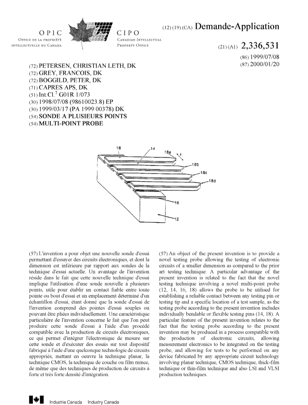
Figure 13, shows probe geometry having tips extending from probe arms;
Figure 14, shows general tip configurations. (a), shows 2-tip, (b), shows 4-
tip having
non-uniform tip spacing, (c), shows 4-tip, (d)-(f), shows (a)-(c) having
secondary
tips;
Figure 15, shows tip fabrication of probe. (a), shows initial view. A tip is
grown on
probe arm 1. (b), shows the sample rotated/tilted hereby obtaining a mirrored
view.
A tip is grown on probe arm 2 on the pointing line of tip 1. (c)-(d), shows
the result
of repeating the procedure until the gap G is slightly larger than the
intended gap
G'. (e), shows the sample rotated to obtain a frontal view, however
additionally tilted
to obtain the chosen angle a' of the secondary tips. (f)-(g), shows the
secondary
CA 02336531 2001-O1-03
WO 00!03252 1 ~ PCT/DK99/00391
tips grown on both tip ends. (h), shows the intended gap G' and the lengths
tuned
by repeating steps (f)-(g).
Figure 16, shows scanning electron microscope pictures of the fabrication
sequence (identical to figure 15). (a)-(c), shows initial growth of tip 1 and
2. (d)-(f),
shows second iteration. (g)-(I), shows third iteration resulting in gap G' of
300 nm.
{j), shows initial growth of secondary tips. (k), shows the secondary tips
after
narrowing in the gap and fcne tuning the lengths to within 10 nm. (I) Overview
picture of finished probes.
Detailed description of the preferred embodiments.
A preferred embodiment is directed toward making a multi-point probe and is
described with respect to figures 3-6.
Figure 3 shows a wafer 10, for example a section of a semiconductor wafer, in
intermediate state of fabrication. It shows a surface 16 of a substrate 12
covered by
a support layer 14, being electrically isolating, such as silicon oxide. The
deposition
of the support layer 14 can be accomplished by any technique known in the art,
such as chemical vapour deposition (CVD), plasma enhanced CVD (PECVD),
electron cyclotron resonance (ECR) or sputtering. As shown in figure 3, the
support
layer 14 is patterned and etched to form beams with tapered end-points 14a-d.
The
beams are not limited to any particular form or symmetry; they can be of any
geometry with suitable end-points.
The pattern is formed by forming a photoresist pattern (not shown in figure 3)
which
defines the four beams on the top surface of the support layer 14. The
photoresist
pattern is formed by conventional photolithographic photoresist formation,
exposure, development and removal techniques. The support layer is then etched
using any technique known in the art, such as dry etching or wet etching,
until the
unmasked parts of the support layer 14 are removed from the top surface of the
substrate.
CA 02336531 2001-O1-03
WO 00/03252 1$ PCT/DK99/00391
In an alternative embodiment of the present invention the four beams or part
of
them can be defined using high-resolution lithographic methods such as
electron-
beam lithography, atomic force microscopy (AFM) lithography or laser
lithography.
Once the support layer has been patterned, the substrate is partially removed
to
release the patterned support layer, forming four cantilevers with sharpened
end-
points 14a-d, as illustrated in figure 4.
In the preferred embodiment, the substrate is removed by depositing a
protective
layer (not shown in figure 4) of silicon nitride on top and bottom surface of
the
substrate 12. Next, a photoresist pattern is formed on the bottom surface of
the
substrate by conventional photolithographic photoresist formation, exposure,
development and removal techniques. The nitride layer is then removed in the
unmasked areas on the bottom surface of the substrate using Reactive Ion Etch
(RIE) in a plasma containing SFs and OZ or similar reagents, and the substrate
is
etched using an etching chemistry comprising potassium hydroxide (KOH) or a
similar chemistry until the freely extending probe arms are exposed. Then the
protecting layer of nitride is removed from the top surface of the substrate
using
RIE, or using wet etching with a chemistry comprising phosphoric acid (H3P04)
or a
similar chemistry.
Figure 5, illustrates the etching of the substrate 12 to undercut the support
layer 14.
In the preferred embodiment, this etching step is performed with a dry etching
method, such as an isotropic RIE etch.
The final stage of fabrication is shown in figure 6, and involves the
deposition of an
electrically conducting layer 18 on the top surface of the wafer. The
conducting
layer is made of conducting materials like Au, Ag, Pt, Ni, Ta, Ti, Cr, Cu, Os,
W, Mo,
Ir, Pd, Cd, Re, conductive diamond, metal silicides or combinations thereof.
Alternatively the conducting layer can be made of a highly doped
semiconducting
material. The conducting layer can be deposited using electron-beam
evaporation,
or any other similar technique known in the art. Due to the undercutting of
the
support layer 14, the electrically conducting layer will not create conducting
paths
CA 02336531 2001-O1-03
WO 00/03252 19 PCT/DK99/00391
between the four beams made in the support layer, and thus tour isolated
electrodes are formed on the top surface of the support beams, and thus points
18a-d can be connected through the beams to an external positioning and
measuring device (not shown in figure 6).
As shown in figure 6 the deposition of the conducting layer creates electrodes
on
the substrate. In a preferred embodiment these electrodes are used for active
guarding of the conductive probe arms to significantly reduce leakage
resistance
and, consequently, increase the measuring accuracy of the invention.
Referring again to figure 6, in the present invention the minimum probe end-
point
separation s is approximately 1 Vim. The minimum probe end-point separation is
however determined by the current state of the art in micro-fabrication
technology
and not any limitation of the present invention. Thus, as micro-fabrication
technology produces smaller and smaller devices, the minimum probe end-point
separation s can also be reduced.
In operation an external positioning device places a multi-point probe made
according to the present invention into physical contact with the surface of
the test
sample. Once electrical contact between the surface of the test sample and all
four
conductive probe arms has been achieved, a current is applied to two of the
conductive probe arms and a corresponding voltage is measured between the two
other conductive arms. The method for applying the current and detecting the
voltage can be any method known in the art.
The preferred embodiment of the multi-point testing apparatus of the present
invention is shown in figure 7. The figure depicts a multi-point testing
apparatus
100, a test sample 110 is mounted on a stage 112 with an XYZ positioning
mechanism. This mechanism can be controlled automatically or manually. A multi-
point probe made according to present invention 102 is mounted above the
surface
of the test sample on a probe holder 104 which can be moved in the Z direction
with
a resolution of 0.1 ~m or better. Optionally the probe holder 104 can be
controlled
with similar spatial resolution in the X and Y directions. The set-up 100 is
similar to
CA 02336531 2001-O1-03
WO 00/03252 2~ PCT/DK99/00391
that of an AFM or a Scanning Tunnelling Microscope (STM). Connections 114 from
the probe end-points are input to a controller 106, which can move the multi-
point
probe with respect to the test sample 110. Optionally a connection 196 from
the test
sample 110 can also be input to the controller 106. The controller 106 can be
a
computer or a programmed micro-controller. By monitoring the four point
resistance
using the end-points of the four probe arms or the two point resistances
between
the end-points of the four probe arms and the test sample 110, the controller
106
can move the multi-point probe towards the test sample until all end-points of
the
four probe arms are in physical contact with the test sample. By holding the
multi-
point probe having the probe arm lengths in an angle relative to the surface
of the
test sample 110, smaller than perpendicular and larger than parallel, full
individual
probe arm flexibility is achieved, providing a safe mode of operation in
regards to
avoiding destruction of single devices on top surface of test sample. Then a
measurement can be made of the test sample resistivity, and the controller 106
analyses the measured data and displays measurement information on display
908.
The controller 106 may retract the multi-point probe, move the test sample 110
in
the XY plane and repeat the procedure.
Figure 8 illustrates a similar apparatus 200 where the test sample stage
consists of
a XY positioned 222 on a standard optical microscope 214. A multi-point probe
made in accordance to the present invention 202 is placed on a probe holder
204,
which is mounted on a microscope objective 212, allowing the operator to
identify
features on the test sample surface and perform four point probe measurements
at
these features. In this manner ~m sized test sample features such as single
microelectronic devices or polycrystalline grains can be probed in a
controlled
fashion. Similar to the previously described apparatus 100, illustrated in
figure 7,
the four leads 218 from the probe are input to a controller 206 as well as a
lead 216
connecting to the test sample; the controller outputs signals 220 controlling
the
movement of the probe holder, and the controller 206 analyses and presents the
measurement data on display 208.
Figure 9, pictures a detachable multi-point probe in a semi-conducting wafer.
A
wafer can consist of several multi-point probes, which are detachable from the
CA 02336531 2001-O1-03
WO 00/03252 21 PCT/DK99/00391
wafer. This production technique provides an extremely repeatable and safe
method of fabrication of multi-point probes.
Figure 10, shows a principal diagram of the circuit used for performing
measurements, comprising an electrometer and a current source. Applying
integrated circuit techniques for the fabrication of multi-point probes
enables the
possible integration of the electrometer, current source and additional
circuit on the
wafer.
A particular preferred embodiment of the present invention utilises electron
beam
deposition techniques for growing tips on probe arms. Figure 11 (a), shows
such an
electron beam deposition grown from a surface 1105 of a probe arm having the
electron beam 1103 in a perpendicular relation to the surface thus creating a
primary tip 1101 having an axis perpendicular to surface plane. By tilting an
electron beam 1115 in relation to a surface 1113 a tilted electron beam
deposition
grows either on the surface 1113 of substrate as a primary tip 1111 or as a
secondary tip 1109 in continuation on top of a previously produced tip 1107
perpendicular to the surface 1113.
The electric properties of the tips may be modified by applying contaminants
1203
to a tip 1201 utilising an injection of metallo-organic compound at low
partial
pressure, hereby obtaining tips with resistances as low as 900 S2 (in-situ
metallization). The electric properties of the tips may also be modified by
applying
a metallic cloud or evaporation 1209 creating metallic layers 1205,1207 on the
tip
1201 and on the surface 1105 subsequent to finalising the tip growth (ex-situ
metallization). By applying subsequent evaporations 1209 using two or more
application angles a good metallic coverage of the tip 1101 and the surface
1105
are achieved, thus providing useful tips 1101. Figure 12, shows both methods
for
metallization of tips.
The geometry of a probe is shown in Figure 13 in top view, side view and front
view. The probe is shown having to probe arms 1301 on to which primary tips
1303
have been grown by utilising electron beam deposition. The primary tips 1303
CA 02336531 2001-O1-03
WO 00/03252 22 PCT/DK99/00391
create an angle 1307 (a1) between direction of axial length of the probe arm
1301
and direction of axial length of primary tips 1303. Secondary tips 1305 extend
from
the primary tips 1303 on the probe arms 1301. The primary tips 1303
furthermore
have an inclination 1309 (~31 ) and the secondary tip 1305 and additional
inclination
1311 ((i2) in relation to the direction of the axial length of the probe arm
1301.
Several tip configurations are shown in figure 14. Figure 14 (a) shows four
parallel
probe arms, two outer probe arms 1401 and the two inner probe arms 1301 having
two primary tips 1303 positioned on the two inner probe arms 1301. The two
primary tips 1303 create an angle in relation to axial direction of the inner
probe
arms 1301 such that the primary tips 1303 point a common orientation. Figure
14
(b) shows the four parallel probe arms 1301,1401 having four primary tips
1303,1403 positioned so that the end point have equal tip separations. Figure
14
(c) shows the four probe arms 1301,1401 each having primary tips 1303,1403
extending from distal end. The two inner probe arms 1301 having the primary
tips
1303 pointing toward a common orientation and the two outer probe arms 1401
pointing toward in axial direction of the outer probe arms 1401. Figures 14
(d) to (f)
show secondary tips 1305,1405 added to the primary tips 1303,1403.
The fabrication scheme for producing primary and secondary tips applying
electron
beam deposition is shown in figure 15. Figure 15 (a) shows the two probe arms
1301 having distal ends defined as 1501 and 1505. The electron beam is aimed
at
a corner 1503 of the surface of the distal end 1505, hereby producing the
primary
tip 1303. As shown in figure 15 (b) the electron beam is subsequently aimed at
a
corner 1507 of the surface of the distal end 1501, hereby producing the second
primary tip 1301. This procedure is repeated until the separation between the
two
primary tips 1301 is slightly larger than the intended gap G' between the
primary
tips 1301. The primary tips 1303 create an angle in relation to axial
direction of
probe arms 1301 and an angle in relation to the surfaces of the distal ends
1501,1505 such that the primary tips 1303 point away from the supporting body
of
the multi-point probe. The secondary tips 1305 furthermore create an angle in
relation to axial direction of the primary tips 1303. In order to achieve this
secondary
CA 02336531 2001-O1-03
WO 00/03252 23 PCT/DK99/00391
angling of the secondary tips 1305 in relation to the primary tips 1301 the
multi-
point probe is rotated as shown in figure 15(e).
Figure 16, shows electron microscope pictures of the fabrication scheme
presented
above and in figure 15.
Example showing the usage of the multi-point probe.
The probe chips (illustrated in figure 9) are broken out of the wafers and are
mounted on ceramic dies (5mm x 10mm) with four big thick-film electrode pads,
using epoxy. The conductive probe arms on the silicon chips are connected to
the
pads on the ceramic dies by bonding 25p,m thick gold wires between them, using
a
Kulicke-Soffa wedge-bonding machine.
The ceramic chips are fixed mechanically and contacted electrically on an
aluminium mount, which is machined to fit around a microscope objective on a
Karl-
Suss probe station. The mount allows the conductive probe arms of the multi-
point
probe to be in focus in the middle of the field of view of the microscope. The
test
sample can then be moved into focus using the normal vertical stage of the
microscope. When the test sample is in focus the multi-point probe will
contact the
test sample and a measurement can be performed. This set-up is similar to the
general illustration in figure 8.
Electronics consisting of an electrometer and a current source is built into
the
aluminium mount to minimise the distance between the probe and the
electronics.
This keeps the noise in the measurements at a minimum. The principal diagram
of
the circuit is shown in figure 10. The two inner conductive probe arms of the
multi-
point probe are connected to an electrometer (an instrumentation amplifier)
with an
input impedance of more than 10GS2 and an amplification factor of 5000. The
peripheral two conductive probe arms of the probe are connected to the current
source (a differential voltage to current converter) which delivers an
adjustable
output in the range of 10nA to 11.~A. The current output is proportional to
the voltage
difference V1-V2. These voltages are generated externally by a computer
equipped
CA 02336531 2001-O1-03
WO 00/03252 24 PCT/DK99/00391
with a digital to analogue converter. The same computer detects the output
voltage
Vo of the electrometer through an attached analogue to digital converter.
Batteries
power the circuit in order to make it float with respect to ground.
A measurement is performed by sampling the voltage of the electrometer for
both
polarities of the current, taking the average of the two values. This
averaging
procedure is useful for eliminating thermal drift in the electronics.