Note: Descriptions are shown in the official language in which they were submitted.
CA 02336557 2001-O1-03
WO 00/67291 PCT/US00/40082
MICROFABRICATED TEMPLATE FOR MULTIPLE CHARGED PARTICLE BEAM
CALIBRATIONS AND SHIELDED CHARGED PARTICLE BEAM
LITHOGRAPHY
FIELD OF THE INVENTION
This invention relates to charged particle beam
lithography, and in particular to charged particle beam
lithography using multiple charged particle beams.
BACKGROUND
Manufacturing of integrated circuit devices is dependent
upon the accurate transferring of the patterns onto various
layers on the surface of the semiconductor wafer, which after
processing is sawn to provide the integrated circuit die: These
patterns define the various regions in the integrated circuit
(IC) die and are generally formed by transferring patterns to
the surface of the wafer by a number of different processes,
e.g., photolithography, ion beam lithography, and electron-beam
lithography.
In the case of a single charged particle beam system, a
precise beam of charged particles is directed to a specific
point on the surface of a substrate coated with a layer of
resist sensitive to the incident charged particle beam. The
resist is then developed and the exposed areas either remain or
are removed, defining a pattern on the surface of the wafer.
Subsequent steps etch away the exposed portions of the wafer
surface to define semiconductor features. Charged beam
lithography such as the electron beam lithography is also well
known for fabricating the masks (reticles) used subsequently in
optical lithography for IC fabrication.
In the case of a multiple charged particle beam system,
multiple beams of particles are directed to various die on a
wafer in the same time. Integrated circuits (ICs) are
typically each one die. A typical semiconductor wafer contains
many (for instance hundreds of) such die arranged in a grid.
-1-
CA 02336557 2001-O1-03
WO 00/67291 PCT/US00/40082
Microcolumn is a well known technology in the electron
beam lithography field. A typical electron beam lithography
machine has a single source of electrons, an associated
accelerator (electrostatic) device for accelerating the
S electrons, and a set of elements which are typically coaxial
electro-magnets for focusing the beam onto the substrate.
However, it is known (see e.g., U.S. Patent Nos. 5,155,412 and
5,122,663 assignee IBM and "Electron-Beam Microcolumns for
Lithography and Related Applications," by Chang, T. et al.,
Journal of Vacuum Science Technology Bulletin 14(6), pp. 3774-
3781, Nov./Dec. 1996, incorporated herein by reference) to
provide an array of microcolumns, called a multiple-electron-
beam exposure system, which uses a plurality of charged
particle beams to write identical patterns on a plurality of
die at the same time to thereby improve productivity. Each
individual microcolumn in the multiple-electron-beam exposure
system is a complete electron-beam column having a typical
diameter of approximately 1 to 2 centimeters.
For lithography, microcolumns build on the demonstrated
ability of scanning electron beams to direct-write device
features with critical dimensions down to well below 100nm, and
to perform the essential alignment and overlay of patterns in
multilayer processes. Operating at low beam energies, 1-2 keV,
the microcolumns also have the advantage of not requiring
proximity effect corrections and are significantly more
efficient in resist exposure.
Nevertheless, electron-beam exposure of the resist
generates a net positive or negative electrical charge on the
resist surface, which is normally non-conductive. When not
properly discharged, the electrical charge creates an electric
field which adversely affects the incident electron beam,
causing distortions and beam placement errors. With the demands
put on electron-beam systems by the continually decreasing
feature size of IC devices, such distortions and placement
errors may be detrimental to the system. However, at low
electron beam voltage, it is impractical to use a discharge
-2-
CA 02336557 2001-O1-03
WO 00/67291 PCT/US00/40082
layer, which is typically positioned on top of the resist
layer, due to the lack of penetration of the incident
electrons.
Accordingly, what is needed is suppression of resist
S charging during the exposure process.
Conventional arrayed (microcolumn) lithography is shown in
FIG. 1 (prior arty. One or more columns 106, 108 expose die
102, 104, respectively, which are arranged in a grid pattern on
a wafer 100. Patterns on wafer 100 can be written in either
vector or raster scan modes over a relatively narrow stripe of
about 50-100 }un in width. The patterns are "stitched" using a
laser 112 controlled table 110 moving in synchronism with
pattern writing.
One requirement for parallel multiple charged particle
beam lithography (such as a system based on an array of
electron microcolumns) is intra- and inter-column (or beam)
calibrations so that the patterns are accurately transferred
onto various layers on various die on the semiconductor wafer
surface. For a single writing tool, e.g., a single electron-
beam microcolumn, a set of registration marks is used to align
one pattern layer of metal, insulator, or semiconductor
material on a substrate with another pattern layer to ensure
that features of the successive layers bear the correct spatial
relationship to one another. The features of the registration
marks are typically used to align the substrate with the
lithographic writing tool for optical or direct electron-beam
writing lithography. During the lithography process, the
registration marks are observed and used to properly align the
lithographic pattern with the underlying layer.
A multiple-charged-particle-beam lithographic system
includes multiple writing tools, e.g., a microcolumn array,
each microcolumn being discrete. Therefore, in addition to
intra-column calibrations, inter-column calibrations must be
carried out to coordinate the microcolumns in relation to one
another. The calibrations must not only be accurate but also
efficient for good throughput.
-3-
CA 02336557 2001-O1-03
WO 00/67291 PCT/I1S00/40082
Accordingly, what is also needed is efficient and accurate
calibration of multiple charged particle beams for multiple
charged particle beam lithography.
SUMMARY
In accordance with the present invention, a method, an
associated structure, and an apparatus for in-situ and in-
parallel multiple charged particle beam calibrations and
shielded charged particle beam lithography are provided. A
template opaque to the charged particle beams and defining an
array of membranes is placed above the target substrate, e.g.,
a semiconductor wafer or perhaps a reticle being fabricated.
Each membrane in the template defines a through slot (a portion
transmissive to the electron beam such as an opening) and a set
of registration marks which are located with respect to the
registration marks of ,the other membranes. In other
embodiments, the transmissive portions and registration marks
are defined in the template with no membranes. Patterns are
written onto the resist-coated target substrate through the
slots by the charged particle beams. The registration marks are
used by each individual charged particle beam to perform inter-
charged particle beam calibrations, i.e. positional calibration
relative to other charged particle beams in the charged
particle beam array, as well as intra-charged particle beam
calibrations, i.e. system calibrations for individual charged
particle beams. In one embodiment, the charged particle beams
are electron beams. In another embodiment, the charged
particle beams are ion beams.
The template with its slots allows intra- and inter-
charged particle beam calibrations, and suppresses undesirable
resist charging during the exposure process. The template is,
e.g., of crystalline silicon for ease of fabrication. In one
embodiment, the template is held in close proximity to the
target wafer with a predetermined distance therebetween. In
another embodiment, the membrane is doped such that it "sags"
from the template toward the target substrate. In yet another
-4-
CA 02336557 2001-O1-03
10
WO 00/67291 PCT/US00/40082
embodiment, the membrane is fashioned into a cantilever that is
actuated into contact with the target substrate during
exposure. In another embodiment, the entire template is placed
in contact with the target substrate.
BRIEF DESCRIPTION OF THE DRAWINGS
FIG. 1 shows a prior art arrayed microcolumn exposure
system using one or more microcolumns per die.
FIG. 2A shows multiple charged particle beam lithography
through a template.
FIG. 2B shows an embodiment of the template, where the
through slot is circular.
FIG. 3A shows a system for shielded charged particle beam
lithography.
FIG. 3B shows a capacitive gap sensor.
FIG. 9 shows an embodiment of the template, having a
sagging membrane.
FIG. 5A shows a top plane view of a template having
multiple membrane cantilevers.
FIG. 5B shows a partial side view of the FIG. 5A
structure.
FIG. 6 shows a application of a current in the membrane.
DETAILED DESCRIPTION
The present invention is directed to a calibration method
using a template having in one embodiment a plurality of
membranes each corresponding to an incident charged particle
beam and each defining a through slot and a set of registration
marks, to achieve high positional accuracy and precise
calibration for lithography using multiple charged particle
beams.
The detailed description is directed toward an electron-
beam system. However, the systems and methods described herein
are equally applicable to other charged particle beam systems
such as an ion beam system.
-5-
CA 02336557 2001-O1-03
WO 00/67291 PCT/US00/40082
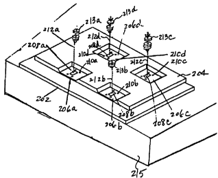
FIG. 2A shows an implementation of multiple electron beam
lithography through such a template. It is understood that the
target substrate (e. g., the wafer) 202 is held on conventional
x-y wafer stage 215 which is a part of the arrayed lithography
system. Stage 215 facilitates wafer movement in synchronism
with pattern writing. The movement of stage 215 is
conventionally controlled by, e.g., laser interferometry
location measurement.
FIG. 2A shows template 204 supporting an array of
membranes 206a, 206b, 206c, 206d, each defining a through slot
208a,. 208b, 208c, 208d, respectively, and a corresponding set
of registration marks 210a, 210b, 210c, 210d that are located
with respect to the other sets of registration marks in the
array, respectively. Template 204 and membranes 206a, 206b,
206c, 206d may be made of, but are not limited to, crystalline
silicon (Si), diamond, silicon carbide (SiC) and thin metallic
foils such as beryllium (Be) and aluminum (A1). In one
embodiment, the membranes are integral parts of template 204.
However, membranes 206a, 206b, 206c, 206d and template 204 need
not be of the same material. Template 204 and membranes 206a,
206b, 206c and 206d are doped to be conductive. Relevant
characteristics of template 204 and membranes 206a, 206b, 206c,
206d are: (1) opacity to electron beams; (2) easily fabricated
to precise dimensions; and (3) conductive.
Silicon has the advantages of manufacturability, strength,
and electric conductivity where necessary. For direct write
lithography on a silicon substrate, silicon template 204 also
provides the advantage of having the same thermal expansion
coefficient as the target silicon wafer 202. As an
alternative, template 204 may be made of any other material
having a similar thermal expansion coefficient as the target
substrate 202, but this is not limiting.
Template 204 is either in "contact mode", i.e., placed in
contact with the substrate of target wafer 202 (target
substrate) or in "proximity mode", i.e., placed in close
proximity to target substrate 202 and there being a
-6-
CA 02336557 2001-O1-03
WO 00/67291 PCT/US00/40082
predetermined distance between template 204 and target
substrate 202 during exposure. For contact mode, template 204
either remains in contact with target substrate 202 or is moved
out of contact during the wafer movement on its stage 606.
Lifting template 204 out of contact with target substrate 202
is achieved by using, for example, piezo actuators 604, as
shown in FIG. 3A. In one embodiment, template 204 is held to
a template stage 606 by clamping the edges of template 204,
above the target substrate stage 215 holding target substrate
202. In an alternative embodiment, template 209 is held to a
template stage 602 by electrostatic means. Piezo actuators 608
move template stage 606 up and down, thus in and out of contact
with target substrate 202. Height reference posts 612 or LED
based height sensing system 610 controls the vertical movement
of piezo actuators 608, as will be discussed in details below.
Proximity mode operation has the advantage of avoiding
possible damage and contamination to template 204 and target
substrate 202. In one embodiment, template 204 is held by an
appropriate template stage 606 (FIG. 3A) as described above and
placed close to target substrate 202 very precisely. The
desired gap between template 204 and target substrate 202
during exposure is maintained, in one embodiment, by pre-
defining a gap using precisely machined height reference posts
612, as shown in FIG. 3A. During exposure, template stage 606,
along with template 204, are pushed by piezo actuators 608
downwards until height reference posts 612 are in contact with
wafer stage 215, or other reference structures. After
exposure, piezo actuators 608 lift template 204 and template
stage 606 upwards for subsequent wafer move.
In another embodiment, the qap between template 204 and
target substrate 202 is measured precisely using an LED-based
height sensing system 610. In this embodiment, the sensor in
LED-based height sensing system 610 references either template
stage 606, template 204, or both, in measuring the gap. In yet
another embodiment, the gap between template 204 and target
substrate 202 is measured precisely using a capacitive gap
CA 02336557 2001-O1-03
WO 00/67291 PCT/US00/40082
sensor 614 (FIG. 3B) located proximate to template 204 and
target substrate 202 to measure the capacitance between
template 204 and target substrate 202. The measured capcitance
is then translated into a gap width.
In one embodiment, each membrane 206a, 206b, 206c, 206d
has dimensions of lmm by lmm or less and a thickness of 1
micron or less. Membranes 206a, 206b, 206c, 206d are
fabricated by conventional micromachining processes well known
in the art, such as a combination of lithography and etching,
to define the thinned out membranes 206, 206b, 206c, 206d and
slots 208a, 208b, 208c, 208d. In one embodiment, temr~late 204
contains as many membranes 206 as there are microcolumns 213 in
the microcolumn array so that each microcolumn 213a, 213b,
213c, 213d is calibrated individually using its own associated
set of registration marks 210. The template 204 is aligned to
the electron beams, e.g., first by a coarse alignment using
mechanical and optical microscopes and then by a fine alignment
using electron beams by monitoring current and detecting
registration marks 210. A typical thickness of template 204
(exclusive of the membrane portions) is approximately 200pm to
approximately 300pm. In one embodiment, the size of template
204 is determined by the size necessary to accommodate the
microcolumn array. In another embodiment, the size of template
204 is the same size as target substrate 202.
Each through slot 208 is formed in the associated membrane
206, for example, by a combination of lithography and dry
etching. Through slot 208 is, e.g., a rectangle shape having a
length slightly longer than the incident electron beam 212 scan
length (e.g. < 100 Eun) and a width slightly larger than the
incident electron beam 212 scan width (e. g. < 10 ~,m). Each
microcolumn 213a, etc. writes a pattern (typically a stripe)
onto the target substrate 202 using the microcolumn's incident
electron beam 212 passing the through slot 208 in membrane 206.
(One reason to have the membrane is to enable fabrication of
the slots by conventional micromachining processes; in some
embodiments, there are slots in the template and no membranes.)
_g_
CA 02336557 2001-O1-03
WO 00/67291 PCT/US00/40082
Template 204 shields exposed areas on the target wafer 202
from incident electron beams 212a, 212b, 212c, 212d after
exposure, thereby suppressing potential resist charging
problems associated with electron beam lithography. This is
because template 204, except for through slots 208a, etc., is
opaque to the incident electron beams 212a, 212b, 212c, 212d.
Template 204 shields exposed areas from incident electron beams
212a, 212b, 212c, 212d after exposure by moving target wafer
202 to the next exposure location following each exposure. In
other words, except for the area under through slots 208a,
208b, 208c, 208d, the resist surface is normally covered by
template 204 during exposure. As a result, through slots 208a,
208b, 208c, 208d in template 204, and incident electron beams
212a, 212b, 212c, 212d are shielded from any electric fields
near the target wafer 202 generated at previously exposed
regions.
To obtain spatial coherence (exact location) in the
placement of registration marks 210a, 210b, 210c, 210b on
membranes 206a, 206b, 206c, 206d, respectively, registration
marks 210a, 210b, 210c, 210d are patterned using, e.g., a
commercially available very precise electron-beam lithography
system or a conventional long-range spatially-coherent
lithography system using conventional interferometric
alignment. Registration marks 210a, etc. are then
transferred, for example, by using an additive technique such
as, but not limited to, lift-off or plating, or a subtractive
technique such as, but not limited to, partial etching of
membranes 206a, etc.
Intra- and inter-column calibrations for positional
accuracy for each microcolumn 213a, etc., i.e. relative to the
other microcolumns in the array and to target wafer 202, are
carried out in-situ (i.e. at the point of exposure) and in
parallel. Calibrating microcolumns 213a, 213b, 213c, 213d in-
situ and in parallel is possible because each microcolumn 213a,
etc. has its own set of registration marks 210a, etc.,
respectively, rather than sharing a set of registration marks.
-9-
CA 02336557 2001-O1-03
WO 00/67291 PCT/IJS00/40082
The spatially coherent registration marks 210 in addition to
facilitate each microcolumn 213 in the microcolumn array to
calibrate itself for positional accuracy relative to each other
as well as to target wafer 202, registration marks 210a, etc.
are also used for system calibrations for individual
microcolumns 213a, etc. such as to correct for drift,
magnification or distortion.
In one embodiment, the sum of the membrane thickness and
the spacing between template 204 and target wafer 202 (if in
proximity mode) is within the focal depth of incident electron
beam 212 of microcolumn 213, which is typically 0.5 to a few
microns. In another embodiment, each electron beam is focused
individually and the calibration is performed with, e.g., each
incident electron beam 212a focused on its respective
registration mark 210a on membrane 206a. The results are then
compensated to account for the difference of the result
obtained from focusing the electron beam 212a in the focal
plane of registration marks 210a and the result obtained from
focusing the electron beam 212a in the focal plane of the
target wafer 202 by computational means. By focusing on
registration marks 210a, the height constraint limited by the
focal depth of incident electron beam 212a is eliminated.
FIG. 2B shows an embodiment of template 204, where through
slot 208 is circular. Through slot 208 may be of other shapes
as well because any arbitrary shapes may be defined by etching
through crystalline structure using reactive ion etching (RIE)
or dry etching. In one embodiment, RIE or dry etching is made
anisotropic (i.e., independent of the crystal direction) to
etch features with straight sidewalls.
FIG. 4 shows an embodiment of the template, having a
"sagging" membrane. Membrane 306 is compressively stressed,
e.g., by doping, such that membrane 306 extends (sags) from
template 304 toward target wafer 302. (A thin crystalline
membrane is known to take on this shape when subject to doping
at appropriate levels so that the crystalline membrane is
conductive.) Sagging membrane 306 allows template 304 to
-10-
CA 02336557 2001-O1-03
WO 00/67291 PCT/US00/40082
maintain a gap from target wafer 302 such that template 304
avoids contact with target wafer 302. Depending on the doping
level and membrane thickness, membrane 306 may or may not come
into direct contact with target wafer 302. In one embodiment,
the entire template surface is doped to a depth equivalent to
the membrane thickness by, e.g., ion-implantation, thermal
diffusion or eiptaxial growth. The microcolumns (not shown)
are calibrated using their respective registration marks 310 as
discussed above. An incident electron beam (not shown) from
the microcolumn then writes a pattern through through slot 308.
FIG. 5A shows a top plane view of a template having
multiple membrane cantilevers. FIG. 5B shows a partial side
view of the FIG. 4A structure. Template 904 is in proximity
mode and membranes 406a, 406b, 406c, 406d are fashioned into
cantilevers 414a, 414b, 414c, 414d, respectively. Membranes
406a, 406b, 406c and 406d are shaped by conventional
lithography and etching process into cantilevers 414a, 414b,
414c and 414d, respectively. A piezo electric material, such
as, but not limited to, tin oxide, is patterned on the back
surface of cantilevers 414a, 414b, 414c, 414d for bending the
cantilevers 414a etc. By fashioning membrane 406 into
cantilever 414, the cantilever 414 portion of template 404 may
be positioned in close proximity to target wafer 402, thus
facilitating wafer movement without the remainder of template
404 coming into contact with target wafer 402.
During exposure, membrane cantilever 414 with its through
slot 408 is actuated into contact with target wafer 402 while
maintaining the gap between template 404 and target wafer 402
by, e.g., application of a voltage. In one embodiment, the
voltage is generated by electrostatic means which generate an
electric field between template 404 and target wafer 402. In
another embodiment, the voltage is generated by piezo electric
means where a piezo electric material is deposited on
cantilever 414 as described above. Cantilever 414 is then
actuated by application of a voltage via, e.g., interconnects
formed using conventional interconnect technology. In one
-11-
CA 02336557 2001-O1-03
WO 00/67291 PCT/US00/40082
embodiment, template 404 is supported above wafer 402 by a
template stage (not shown).
The template may be covered by resist material over time,
thereby giving rise to resist charging problem. This resist
S charging problem may be reduced or eliminated by heating the
template with, for example, an electric current. By passing a
current through the silicon membrane, the membrane is heated
and the resist buildup is burned off. FIG. 6 shows electrodes
500 and 501 having voltage potentials +V and -V, respectively,
connected directly to template 504 on either side of membrane
506. A current I thus flows through membrane 506 from
electrode 500 toward electrode 501. In one embodiment, the
membrane is kept warm to prevent buildup of organic materials.
In an alternative embodiment, the template is removed and
cleaned regularly or on an as-needed basis. In yet another
embodiment, the template is removed and replaced regularly or
on an as-needed basis.
Although the invention has been described with reference
to particular embodiments, the description is only an example
of the invention's application and should not be taken as a
limitation. For example, the above description also applies to
low-energy ion microcolumns and in fabrication of masks
(reticles). Various other adaptations and combinations of
features of the embodiments disclosed are within the scope of
the invention as defined by the following claims.
-12-