Note: Descriptions are shown in the official language in which they were submitted.
CA 02336770 2001-O1-05
WO 00/02241 PCT/US99/15032
VAPOR DEPOSITION ROUTES TO NANOPOROUS SILICA
BACKGROUND OF THE INVENTION
FIELD OF THE INVENTION
The invention relates to nanoporous dielectric films and to a process for
their
manufacture. Such films are useful in the production of integrated circuits.
DESCRIPTION OF THE PRIOR ART
The desire for lower dielectric constant materials for use as intermetal and
interlevel
dielectrics for technology nodes at 0.18 micron feature sizes and below is
well-known
in the semiconductor industry. Although the need for obtaining such films has
been
known for a number of years, commercially available materials have been
limited to a
those having a dielectric constant in the range of k>2.7. Although low
dielectric
constant materials are required, a number of other criteria must also be met
for a
useful dielectric material in the semiconductor uses. These criteria include
electrical
leakage, breakdown, and electromigration; high chemical purity, a six month or
better
storage life, low moisture adsorption, chemical resistance; thickness
uniformity, low
stress, low shrinkage, and crack resistance; high thermal stability, low
thermal
expansion, low thermal weight loss; and low cost. Nanoporous silicas are good
materials which meet these criteria and also offer dielectric constants of 2.7
and
below.
In addition to a low dielectric constant, nanoporous silica offers other
advantages for
microelectronics applications including thermal stability up to 900 °C,
pore sizes
which are smaller than microelectronics features; a material that is widely
used in the
CA 02336770 2001-O1-05
WO 00/02241 PCT/US99/15032
semiconductor industry, namely silica and its precursors; deposition using
tools simiar
to those employed for conventional spin-on glass (SOG) processing; as well as
the
ability to tune dielectric constants over a wide range k= 1.3-2.5. Nanoporous
silicas
also avoid thickness constraints from cracking as observed with conventional
SOG's,
and have the ability to migrate the same dielectric material and integration
scheme for
multiple semiconductor technology nodes by tuning the dielectric constant to
lower
values. Although nanoporous silica has these advantages, it also rnay suffer
from
several disadvantages which are common to most SOG materials. These include a
relatively large raw material consumption. For a 200 mm wafer, 3 to 8 cm3 of
silica
precursor is typically deposited for each dielectric layer. However, the
actual volume
of the film is on the order of 0.1 cm3. Therefore, a significant fraction of
the silica
precursor is lost which results in higher costs to the IC manufacturer. A
large volume
of solvent is typically used in SOG and nanoporous silica precursors in order
to lower
viscosity for deposition. However, the evaporation of the solvent results in a
concentration of impurities in the film. As IC dimensions continue to shrink,
IC
manufacturers require ever lower impurity levels which thus require the use of
extremely pure solvents which adds a nontrivial expense to the precursor
production.
As a result of changes in fluid dynamics and mass transfer across the wafer,
the
problem of achieving film uniformity, thickness and refractive index can be
difficult.
This problem becomes more difficult as substrate sizes increase and for
nonuniform
shapes such as flat panel displays. Often, spin-on materials suffer from the
appearance
of a number of different kinds of film defects arising from the complex drying
and
polymerization processes. Furthermore, the extent of local and global
planarization
depends on a complex interrelationships among a number of variables. Using a
2S deposition technique other than spin deposition could result in different
planarization
results.
This invention solves the above problems by depositing a nanoporous silica
precursor
on a wafer by condensation of silica presursors from the vapor phase. In this
way,
essentially all of the precursor is transformed into silica, resulting in much
higher
2
CA 02336770 2001-O1-05
WO 00/02241 PCT/US99/15032
yields, lower solvent consumption, and higher purity. In addition, the film
uniformity
is better than for films deposited by a liquid spin-on glass technique.
According to the invention, a silica precursor is deposited onto the wafer
from a
vapor. This may be conducted by silica precursor deposition from the vapor
phase to
form a liquid-like film on the wafer surface. This may also include co-
deposition from
the vapor phase of a solvent, and/or solvent vapor deposition before or after
the silica
precursor. Polymerization and gelation caused by exposure of the silica
precursor to
an initiator or catalyst such as an acidic or basic vapor, water vapor,
thermal means,
light or other means that cause gelation. This intermediate product is a wet
gel film in
which the pores of the film contain a fluid which can be removed by subsequent
drying. Drying the polymerized film then yields a porous silica film with pore
size on
the order of nanometers. Additional optional steps may include a treatment to
make
the film hydrophobic, a heat treatment before polymerization to aid in
planarization
and gap filling, i.e. reflow, and/or aging and thermal curing before or after
drying to
increase film strength.
SUMMARY OF THE INVENTION
The invention provides a process for forming a nanoporous dielectric coating
on a
substrate which comprises
a) vaporizing at least one alkoxysilane composition;
b) depositing the vaporized alkoxysilane composition onto a substrate;
c) exposing the deposited alkoxysilane composition to a water vapor, and
either an
acid or a base vapor; and
d) drying the exposed alkoxysilane composition, thereby forming a relatively
high
porosity, low dielectric constant, silicon containing polymer composition on
the
substrate.
The invention also provides a semiconductor device produced by a process which
comprises
3
_ .~__ __ _. _
CA 02336770 2001-O1-05
WO 00/02241 PCT/US99/15032
a) vaporizing at least one alkoxysilane composition;
b) depositing the vaporized alkoxysilane composition onto a semiconductor
substrate;
c) exposing the deposited alkoxysilane composition to a water vapor, and
either an
acid or a base vapor; and
d) drying the exposed alkoxysilane composition, thereby forming a relatively
high
porosity, low dielectric constant, silicon containing polymer composition on
the
semiconductor substrate.
BRIEF DESCRIPTION OF THE DRAWING
Figure 1 shows a schematic representation of an apparatus suitable for
conducting the
process of the invention.
DETAILED DESCRIPTION OF THE PREFERRED EMBODIIVVIENT
In the inventive process, one begins by vaporizing at least one alkoxysilane
composition. The alkoxysilane comprises one or more components selected from
the
group consisting of alkoxysilanes having the formula:
R
R-Si-R
R
wherein at least 2 of the R groups are independently C, to C4 alkoxy groups,
alkylalkoxy groups wherein the alkyl moiety is C, to Ca alkyl and the alkoxy
moiety is
C~ to C6 alkoxy, or ether-alkoxy groups; and the balance, if any, are
independently
selected from the group consisting of hydrogen, alkyl, phenyl, halogen,
substituted
4
_ _._ _....__ ?.._ _._ __
CA 02336770 2001-O1-05
WO 00/02241 PCT/US99/15032
phenyl. In one preferred embodiment each R is methoxy, ethoxy or propoxy. In
another preferred embodiment at least two R groups are alkylalkoxy groups
wherein
the alkyl moiety is C, to C4 alkyl and the alkoxy moiety is C1 to C6 alkoxy.
In yet
another preferred embodiment at least two R groups are ether-alkoxy groups of
the
formula (C, to C6 alkoxy)" wherein n is 2 to 6.
The silica precursor could be any or a combination of alkoxysilanes such as
tetraethoxysilane, tetrapropoxysilane, tetraisopropoxysilane,
tetra(methoxyethoxy)silane, tetra(methoxyethoxyethoxy)silane which have four
groups which may be hydrolyzed and than condensed to produce silica,
alkylalkoxysilanes such as methyltriethoxysilane silane, arylalkoxysilanes
such as
phenyltriethoxysilane and precursors such as triethoxysilane which yield SiH
functionality to the film. Tetrakis(methoxyethoxyethoxy)silane,
tetrakis(ethoxyethoxy)silane, tetrakis(butoxyethoxyethoxy)silane, tetrakis(2-
ethylthoxy)silane, tetrakis(methoxyethoxy)silane, and
tetrakis(methoxypropoxy)silane
are particularly useful for the invention. Additionally, partially hydolyzed,
condensed
or polymerized derivatives of these species can be used in this invention.
Other
precursors of utility to this invention could include precursors which can be
thermally
or photolytically crossIinked. In general, the precursors can be gases,
liquids or solids
at room temperature.
The silica precursor composition may optionally comprise a solvent
composition,
water and/or a catalytic amount of an acid. Water provides a medium for
hydrolyzing
the alkoxysilane. Preferably the solvent composition can comprises a
relatively high
volatility solvent or a relatively low volatility solvent. A relatively high
volatility
solvent is one which preferably has a boiling point of about 120 °C or
less, preferably
about 100 °C or less. Suitable high volatility solvents nonexclusively
include
methanol, ethanol, n-propanol, isopropanol, n-butanol and mixtures thereof.
Other
relatively high volatility solvent compositions which are compatible with the
other
ingredients can be readily determined by those skilled in the art.
CA 02336770 2001-O1-05
WO 00/02241 PCT/US99/15032
A relatively low volatility solvent composition is one which preferably has a
boiling
point of about 175 °C or higher, more preferably about 200 °C or
higher. Suitable low
volatility solvent compositions nonexclusively include alcohols and polyols
including
glycols such as ethylene glycol, 1,4-butylene glycol, 1,5-pentanediol, 1,2,4-
butanetriol, 1,2,3-butanetriol, 2-methyl-propanetriol, 2-(hydroxymethyl)-1,3-
propanediol, 1,4,1,4-butanediol, 2-methyl-1,3-propanediol, tetraethylene
glycol,
triethylene glycol monomethyl ether, glycerol and mixtures thereof. Other
relatively
low volatility solvent compositions which are compatible with the other
ingredients
can be readily determined by those skilled in the art.
The optional acid serves to catalyze the reaction of the alkoxysilane with the
relatively
high volatility solvent, relatively low volatility solvent and water. Suitable
acids are
nitric acid and compatible organic acids which are volatile, i.e. which
evaporate from
the resulting reaction product under the process operating conditions, and
which do
not introduce impurities into the reaction product. Preferably the precursor
components are purified, such as by distillation such that the alkoxysilane
composition has no more than about 250 parts per billion of trace metal
impurities.
The alkoxysilane component is preferably present in an amount of from about 3
% to
about 100 % by weight of the precursor composition. A more preferred range is
from
about 20 % to about i00 % and most preferably from about 50 % to about 100 %.
The solvent component may be present in an amount of from about 0 % to about
95 %
by weight of the precursor composition. A more preferred range is from about 0
% to
about 80 % and most preferably from about 0 % to about 50 %. While the
precursor
somposition can contain more than one solvent, it is preferred that it not
contain both a
high and a low volatility solvent. It is preferred that the solvent or solvent
mixture
evaporate at a relatively constant rate. In the alternative, one or more
solvents can be
applied singly, sequentially or in mixture to the substrate prior to the
application of the
6
CA 02336770 2001-O1-05
WO 00!02241 PCTNS99/15032
alkoxysilane or after the application of the alkoxysilane. Such can aid
precursor
viscosity, pore control, or to help the miscibility of water vapor into the
silane.
When both a high and a low volatility solvent are applied in a mixture prior
to the
application of the alkoxysilane or after the application of the alkoxysilane,
the high
volatility solvent component may present in an amount of from about 1 % to
about 90
% by weight of the precursor composition. A more preferred range is from about
1 % to
about 50 % and most preferably from about i % to about 30 %. When both a high
and a
low volatility solvent are present, the low volatility solvent component may
be present in
an amount of from about 1 to about 40 % by weight of the precursor
composition. A
more preferred range is from about 1 % to about 20 % and most preferably from
about 1
% to about 10 %.
The mole ratio of water to silane may be from about 0 to about 50. A more
prefezred
range is from about 0 to about 10 and most preferably from about 0 to about
1.5. The
acid is present in a catalytic amount which can be readily determined by those
skilled
in the art. Preferably the molar ratio of acid to silane ranges from about 0
to about
0.2, more preferably from about 0 to about 0.05, and most preferably from
about 0 to
about 0.02.
The alkoxysilane containing precursor composition is then deposited onto a
substrate,
preferably a semiconductor substrate, optionally having a pattern of lines on
its
surface and forms a dielectric film on the surface. Typical substrates are
those suitable
to be processed into an integrated circuit or other microelectronic device.
Suitable
substrates for the present invention non-exclusively include semiconductor
materials
such as gallium arsenide (GaAs), silicon and compositions containing silicon
such as
crystalline silicon, polysilicon, amorphous silicon, epitaxial silicon, and
silicon
dioxide (Si02) and mixtures thereof. The lines, when present, are typically
formed by
well known lithographic techniques and may be composed of a metal, an oxide, a
nitride or an oxynitride. Suitable materials for the lines include silica,
silicon nitride,
7
.~.__. _ _..
CA 02336770 2001-O1-05
WO 00/02241 PCT/US99/15032
titanium nitride, tantalum nitride, aluminum, aluminum alloys, copper, copper
alloys,
tantalum, tungsten and silicon oxynitride. These lines form the conductors or
insulators of an integrated circuit. Such are typically closely separated from
one
another at distances of about 20 micrometers or less, preferably 1 micrometer
or less,
and more preferably from about 0.05 to about 1 micrometer.
For deposition on the substrate, the precursor composition is vaporized in any
of
several ways such as by flowing an inert carrier gas, such as nitrogen, past
the
precursor into a deposition chamber or by heating the precursor relative to
the
substrate temperature. An apparatus suitable for depositing the precursor is
shown
schematically in Figure 1 and described more fully hereinafter. Other suitable
apparatus can easily be determined by those skilled in the art. In general,
the
precursor temperature is raised significantly above the temperature of the
substrate to
allow adequate deposition rates. The precursor is preferably vaporized by
heating the
alkoxysilane composition to a temperature of from about 0 °C to about
300 °C,
preferably from about 150 °C to about 240 °C and more preferably
from about 200 °C
to about 220 °C.
The vaporized precursor is deposited onto the substrate by allowing the inert
carrier
gas to carry the vaporized precursor onto the substrate where it forms into a
uniform
layer on the substrate. It is desirable that the precursor be a liquid at the
substrate
temperature although the substrate can be subsequently heated to liquefy the
precursor
film on the wafer. The reaction chamber must be designed in such a way such
that
uniform deposition is obtained. Such techniques are well-known to those
skilled in
the art of vapor deposition. Either before or after precursor deposition, it
may be
desirable to also deposit a solvent to create porosity in the precursor. More
desirable is
to create the solvent in-situ by hydrolyzing groups from the precursor.
Whether using
added solvent or solvent added in-situ, it is desirable that the volume
fraction of
solvent in the film be approximately equal to the volume fraction of porosity
desired
in the final film.
CA 02336770 2001-O1-05
WO 00/02241 PCT/US99/15032
Depending upon the precursor employed, gelation/polymerization is next
initiated.
The reaction product is hydrolyzed and condensed until it forms a gel layer.
For
example, this could be undertaken by flowing a stream of water vapor and an
acid
vapor or base vapor such as ammonia past the substrate. For purposes of this
invention, a base vapor includes gaseous bases. Preferably the coating is
first exposed
to a water vapor and then exposed to the acid vapor or the base vapor,
however, in an
alternate embodiment, the coating may first be exposed to the acid vapor or
the base
vapor and then the water vapor. The exposures may be conducted at atmospheric
pressure, sub-atmospheric pressure or super-atmospheric pressure. Suitable
bases for
use in the base vapor nonexclusively include ammonia and amines, such as
primary,
secondary and tertiary alkyl amines, aryl amines, alcohol amines and mixtures
thereof
which have a boiling point of about 200 °C or less, preferably 100
°C or less and more
preferably 25 °C or less. Preferred amines are methylamine,
dimethylamine,
trimethylamine, n-butylamine, n-propylamine, tetramethyl ammonium hydroxide,
piperidine and 2-methoxyethylamine. The ability of an amine to accept a proton
in
water is measured in terms of the basicity constant Kh, and pKb= -log Kb. In
the
preferred embodiment, the pKb of the base may range from about less than 0 to
about
9. A more preferred range is from about 2 to about 6 and most preferably from
about 4
to about 5. Suitable acid vapors nonexclusively include nitric acid and
compatible
organic acids which are volatile, i.e. which evaporate from the resulting
reaction
product under the process operating conditions, and which do not introduce
impurities
into the reaction product.
In the preferred embodiment, the mole ratio of water vapor to acid or base
vapor
ranges from about 1:3 to about 1:100, preferably from about 1:5 to about 1:50,
and
more preferably from about 1:10 to about 1:30.
The water vapor causes a continued hydrolysis of the alkoxysilane alkoxy
groups, and
the acid or base catalyzes condensation of the hydrolyzed alkoxysilane and
serves to
9
CA 02336770 2001-O1-05
WO 00/02241 PCT/US99/15032
increase molecular weight until the coating gels and ultimately increases gel
strength.
Finally, the wafer is heated causing the solvent to be removed. The solvent
evaporates
over a period of seconds or minutes, preferably from about 1 minute to about
10
minutes. The film is dried in a conventional way. Elevated temperatures may be
employed to dry the coating in this step. Such temperatures may range from
about
100 °C to about 600 °C, preferably from about 200 °C to
about 400 °C and more
preferably from about 300 °C to about 350 °C. As a result, a
relatively high porosity,
low dielectric constant, silicon containing polymer composition forms on the
substrate. The silicon containing polymer composition preferably has a
dielectric
constant of from about 1.1 to about 3.5, more preferably from about 1.3 to
about 3.0,
and most preferably from about 1.5 to about 2.5. The pore size of silica
composition
ranges from about 1 nm to about 100 nm, more preferably from about 2 nm to
about
30 nm, and most preferably from about 3 nm to about 20 nm. The density of the
silicon containing composition, including the pores, ranges from about 0.1 to
about
1.9 g/cm3, more preferably from about 0.25 to about 1.6 g/cm3, and most
preferably
from about 0.4 to about 1.2 g/cm3.
For some embodiments of the invention, it may be desirable to react remaining
silanol
groups in the gel with a surface modification agent such as
hexamethyldisilazane. This
may be done by flowing hexamethyldisilazane vapor past the wafer before or
after the
drying step. The following non-limiting examples serve to illustrate the
invention.
EXAMPLES
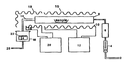
Figure 1 exemplifies a deposition apparatus suitable for conducting the
examples.
The apparatus is comprised of a pipe 2 which is connected to a source of inert
Garner
gas such as nitrogen. The source flow rate of the nitrogen is controlled by a
rotometer
4 and passes through a desiccant 6 to remove any moisture. The pipe connects
to a
precursor sample chamber 8 which is preferably a steel tube which contains the
precursor material which is to be deposited. The chamber is surrounded by a
heating
CA 02336770 2001-O1-05
WO 00/02241 PCT/US99/15032
tape 10 which is controlled by temperature controller 12. A pipe 14 exiting
the
sample chamber carries vaporized precursor and carrier gas to a deposition
chamber
16. Pipe 14 is preferably surrounded by a heating tape 18 which is controlled
by
temperature controller 20. The temperature controllers and heating tapes
uniformly
heat the pipes and sample chamber.
Deposition chamber 16 is preferably a stainless steel container of
approximately six
inches in diameter and 7.5 inches long. It is large enough to contain a 4 inch
silicon
wafer 22 and a steel block 24 which is 4 inches in diameter and 2.5 inches
thick, on
which the wafer 22 sits. This block 24 sits 3 to 4 inches below the exit from
the pipe
14 outlet, which comes through the top of the chamber 16. The wafer 22 is
placed on
top of block 24 such that the gas flow from the pipe 14 impinges directly on
the
surface of the wafer 22. The top and bottom of deposition chamber 16 separate
so the
block 24 and the wafer 22 can be placed inside. When the deposition chamber
top
and bottom are joined, they form an airtight seal. The deposition chamber has
an
outlet 26 at the bottom through which the earner gas can exit to an exhaust
within a
fume hood 28.
EXAMPLE 1
This example illustrates a process wherein a precursor,
tetrakis(methoxyethoxyethoxy)-silane is deposited in the vapor phase onto a
silicon
wafer which is then aged for a given period of time and dried.
The precursor is tetrakis(methoxyethoxyethoxy)-silane (Gelest Inc., Tullytown,
PA).
This precursor material is distilled to remove the impurity (2-(2-
methoxyethoxy)ethanol) which is found in quantities of up to 5 °lo by
weight in the
silane. The distillation was accomplished by placing 5 ml of the precursor in
a
crucible and placing the crucible in the steel tube and heating to
240°C for 5 hours,
while flowing dry nitrogen gas through the tube at 100 cc/minute, and out the
exhaust
11
CA 02336770 2001-O1-05
WO 00/02241 PCT/US99/15032
at the bottom of the deposition chamber. The wafer and block are not in the
chamber
while the precursor is distilled.
The distilled precursor was deposited as follows. The pipe in which the
precursor was
placed was heated using its temperature controller 12 to 240°C, the
connecting tube
was heated to 246°C using temperature controller 20. The block was
cooled to 5°C,
placed in the chamber so that it was 4 inches below the top of the chamber
when the
top and bottom are attached. A blank 4 inch silicon wafer was placed on top of
the
block and the chamber was closed. The nitrogen flow was turned on at a rate of
200
cc/minute and allowed to flow for 5 minutes.
Next the chamber was opened and the wafer was removed and placed into an aging
chamber (a sealable chamber with a volume of ~ 1 liter) with 5 ml ammonium
hydroxide 28-30%, sealed and left for 8 minutes. The wafer was then removed
from
the chamber and dried in an oven at 170°C for 10 minutes, followed by 2
minutes in a
320°C oven. The film deposited on the wafer was approximately 3 cm in
diameter
and at the center of the wafer. The film was characterized by ellipsometry to
have an
average thickness of 2500 angstroms and an average refractive index of 1.108,
which
corresponds to a density of 0.52 g/cc.
EXAMPLE 2
This example illustrates a process wherein a precursor,
tetrakis(methoxyethoxyethoxy)-silane is deposited in the vapor phase onto a
silicon
wafer which is then aged for a given period of time and then dried. In this
example,
the nitrogen flow rate is increased and allowed to flow for a longer time to
increase
the rate of deposition.
12
CA 02336770 2001-O1-05
WO 00/02241 PCTNS99/15032
The precursor is tetrakis(methoxyethoxyethoxy)-silane. This precursor material
is
distilled to remove the impurity (2-(2-methoxyethoxy)ethanol) which is found
in
quantities of up to 5 % by weight in the silane. The distillation was
accomplished by
placing 5 ml of the precursor in a crucible and placing the crucible in the
steel tube
and heating to 240°C for 5 hours, while flowing dry nitrogen gas
through the tube at
100 cc/minute, and out the exhaust at the bottom of the deposition chamber.
The
wafer and block are not in the chamber while the precursor is distilled.
The distilled precursor was deposited as follows. The pipe in which the
precursor was
placed was heated using temperature controller 12 to 240°C, the
connecting tube was
heated to 246°C using temperature controller 20. The block was cooled
to 6°C,
placed in the chamber so that it was 4 inches below the top of the chamber
when the
top and bottom are attached. A blank 4 inch silicon wafer was placed on top of
the
block and the chamber was closed. The nitrogen flow was turned on at a rate of
300
cc/minute and allowed to flow for 15 minutes. Next the chamber was opened and
the
wafer was removed and placed into an aging chamber (a sealable chamber with a
volume of ~1 liter) with 5 ml ammonium hydroxide 28-30%, sealed and left for
10
minutes. The wafer was then removed from the chamber and dried in an oven at
170°C for 10 minutes, followed by 2 minutes in a 320°C oven. The
film deposited on
the wafer was approximately 4 cm in diameter and at the center of the wafer.
The film
was characterized by ellipsometry to have an average thickness of 6250
angstroms and
an average refractive index of 1.093 which corresponds to a density of 0.45
g/cc.
This film was examined by SEM and shown to be porous and of a thickness of
approximately 6250 angstroms.
EXAMPLE 3
This example illustrates a process wherein a precursor,
tetrakis(methoxyethoxyethoxy)-silane is deposited in the vapor phase onto a
silicon
13
CA 02336770 2001-O1-05
WO 00/02241 PCTNS99/15032
wafer which is then aged for a given period of time and then dried. In this
example the
nitrogen flow rate is held constant (300 cc/min.) and allowed to flow for a
longer time
(30 min.) to increase the deposition.
The precursor is distilled tetrakis(methoxyethoxyethoxy)-silane. In this
example the
precursor material is the same as that distilled and used in Example 2. The
distilled
precursor was deposited as follows. The pipe in which the precursor was placed
was
heated using temperature controller 12 to 240°C, the connecting tube
was heated to
246°C using temperature controller 20. The block was cooled to
8°C, placed in the
chamber so that it was 4 inches below the top of the chamber when the top and
bottom
are attached. A blank 4 inch silicon wafer was placed on top of the block and
the
chamber was closed. The nitrogen flow was turned on at a rate of 300 cc/minute
and
allowed to flow for 30 minutes. Next the chamber was opened and the wafer was
removed and placed into an aging chamber (a sealable chamber with a volume of
~1
liter) with 5 ml ammonium hydroxide 28-30%, sealed and left for 10 minutes.
The
wafer was then removed from the chamber and dried in an oven at 170°C
for 10
minutes, followed by 2 minutes in a 320°C oven. The film deposited on
the wafer
was approximately 4 cm in diameter and at the center of the wafer. The film
was
characterized by ellipsometry to have an average thickness of 9400 angstroms
and an
average refractive index of 1.125 which corresponds to a density of 0.60 g/cc.
EXAMPLE 4
This example illustrates a process wherein a precursor, tetrakis(ethoxyethoxy)-
silane
is deposited in the vapor phase onto a silicon wafer which is then aged for a
given
period of time and then dried.
The precursor is tetrakis(ethoxyethoxy)-silane. This precursor material is
distilled to
remove the impurity (2-(2-ethoxy)ethanol) which is found in quantities of up
to 5 %
14
_ __ _ _._.__ .~._. _. _ _
CA 02336770 2001-O1-05
WO 00/02241 PCT/US99/15032
by weight in the silane. The distillation was accomplished by placing S ml of
the
precursor in a crucible and placing the crucible in the steel tube and heating
to 230°C
for S hours while flowing dry nitrogen gas through the tube at 100 cc/minute,
and out
the exhaust at the bottom of the deposition chamber. The wafer and block are
not in
S the chamber while the precursor is distilled. The distilled precursor was
deposited as
follows. The pipe in which the precursor was placed was heated using
temperature
controller 12 to 230°C, the connecting tube was heated to 23S°C
using temperature
controller 20. The block was cooled to 6°C, placed in the chamber so
that it was 4
inches below the top of the chamber when the top and bottom are attached. A
blank 4
inch silicon wafer was placed on top of the block and the chamber was closed.
The
nitrogen flow was turned on at a rate of 400 cc/minute and allowed to flow for
20
minutes.
Next the chamber was opened and the wafer was removed and placed into an aging
1S chamber (a sealable chamber with a volume of ~1 liter) with S ml ammonium
hydroxide 28-30%, sealed and left for 10 minutes. The wafer was then removed
from
the chamber and dried in an oven at 170°C for 10 minutes, followed by 2
minutes in a
320°C oven.
The film deposited on the wafer covered the entire wafer and had a central
spot that
was approximately 4 cm in diameter and at the center of the wafer cracked and
flaked
off during the drying process. The remaining film outside the central spot was
characterized by ellipsometry to have an average thickness of 19,400 angstroms
and
an average refractive index of 1.265 which corresponds to a density of 1.26
g/cc.
2S
EXAMPLE S
This example illustrates a process wherein a precursor, tetrakis(ethoxyethoxy)-
silane
is deposited in the vapor phase onto a silicon wafer which is then aged for a
given
1S
.. __. ...,._~ __ ______ ___-...
CA 02336770 2001-O1-05
WO 00/02241 PCT/US99/15032
period of time and then dried. In this example, the deposition conditions are
changed
in the deposition apparatus to have an a final effect on the over-all
deposition.
The precursor is tetrakis(ethoxyethoxy)-siiane. In this example the precursor
material
is the same as that distilled and used in Example 4.
The distilled precursor was deposited as follows The pipe in which the
precursor was
placed was heated using temperature controller 12 to 235°C, the
connecting tube was
heated to 240°C using temperature controller 20. The block was cooled
to 8°C,
placed in the chamber so that it was 4 inches below the top of the chamber
when the
top and bottom are attached. A blank 4 inch silicon wafer was placed on top of
the
block and the chamber was closed. The nitrogen flow was turned on at a rate of
400
cc/minute and allowed to flow for 10 minutes. Next the chamber was opened and
the
wafer was removed and placed into an aging chamber (a sealable chamber with a
volume of ~ 1 liter) with 5 ml ammonium hydroxide 28-30%, sealed and left for
10
minutes. The wafer was then removed from the chamber and dried in an oven at
170°C for 10 minutes, followed by 2 minutes in a 320°C oven. The
film deposited on
the wafer covered the entire wafer and had a central spot that was
approximately 4 cm
in diameter and at the center of the wafer cracked and flaked off during the
drying
process. The remaining film outside the central spot was characterized by
ellipsometry to have an average thickness of 22,200 angstroms and an average
refractive index of 1.278 which corresponds to a density of 1.34 g/cc.
EXAMPLE 6
This example illustrates a process wherein a precursor, tetrakis(ethoxyethoxy)-
silane
is deposited in the vapor phase onto a silicon wafer which is then aged for a
given
period of time and then dried. In this example, the deposition conditions are
changed
in the deposition apparatus to have a final effect on the over-all deposition.
16
a .T_~ _
CA 02336770 2001-O1-05
WO 00/02241 PCT/US99/15032
The precursor is tetrakis(ethoxyethoxy)-silane. This precursor material is
distilled to
remove the impurity (2-(2-ethoxy)ethanol) which is found in quantities of up
to 5 %
by weight in the silane. The distillation was accomplished by placing 5 ml of
the
precursor in a crucible and placing the crucible in the steel tube and heating
to 200°C
for 5 hours while flowing dry nitrogen gas through the tube at 100 cc/minute,
and out
the exhaust at the bottom of the deposition chamber. The wafer and block are
not in
the chamber while the precursor is distilled.
The distilled precursor was deposited as follows. The pipe in which the
precursor was
placed was heated using temperature controller 12 to 200°C, the
connecting tube was
heated to 210°C using temperature controller 20. The block was cooled
to 10°C,
placed in the chamber so that it was 4 inches below the top of the chamber
when the
top and bottom are attached. A blank 4 inch silicon wafer was placed on top of
the
block and the chamber was closed. The nitrogen flow was turned on at a rate of
400
cc/minute and allowed to flow for 15 minutes.
Next the chamber was opened and the wafer was removed and placed into an aging
chamber (a sealable chamber with a volume of ~ 1 liter) with 5 ml ammonium
hydroxide 28-30%, sealed and left for 10 minutes. The wafer was then removed
from
the chamber and dried in an oven at 170°C for 10 minutes, followed by 2
minutes in a
320°C oven. The film deposited on the wafer covered the entire wafer.
The film was
characterized by ellipsometry to have an average thickness of 22,000 angstroms
and
an average refractive index of 1.I 12 which corresponds to a density of 0.53
g/cc.
EXAMPLE 7
This example illustrates a process wherein a precursor is deposited in the
vapor phase
onto a silicon wafer which is then aged for a given period of time and then
dried. In
17
CA 02336770 2001-O1-05
WO 00/02241 PCT/US99/15032
this example, the deposition conditions are changed in the deposition
apparatus to
have a final effect on the over-all deposition. The precursor is
tetrakis(ethoxyethoxy)-silane. In this example the precursor material is the
same as
that distilled and used in Example 6.
The distilled precursor was deposited as follows. The pipe in which the
precursor was
placed was heated using temperature controller 12 to 200°C, the
connecting tube was
heated to 210°C using temperature controller 20. The block was cooled
to 8°C,
placed in the chamber so that it was 4 inches below the top of the chamber
when the
top and bottom are attached. A blank 4 inch silicon wafer was placed on top of
the
block and the chamber was closed. The nitrogen flow was turned on at a rate of
400
cc/minute and allowed to flow for 10 minutes. Next the chamber was opened and
the
wafer was removed and placed into an aging chamber (a sealable chamber with a
volume of ~ 1 liter) with 5 ml ammonium hydroxide 28-30%, sealed and left for
10
minutes. The wafer was then removed from the chamber and dried in an oven at
170°C for 10 minutes, followed by 2 minutes in a 320°C oven. The
film deposited on
the wafer covered the entire wafer. The film was characterized by ellipsometry
to
have an average thickness of 19,300 angstroms and an average refractive index
of
1.169 which corresponds to a density of 0.80 gJcc.
EXAMPLE 8
This example illustrates a process wherein a precursor, tetrakis(ethoxyethoxy)-
silane
is deposited in the vapor phase onto a silicon wafer which is then aged for a
given
period of time and then dried. In this example, the deposition conditions are
changed
in the deposition apparatus to have a final effect on the over-all deposition.
The precursor is tetrakis(ethoxyethoxy)-silane. In this example the precursor
material
is the same as that distilled and used in Examples 6 and 7.
18
CA 02336770 2001-O1-05
WO 00/02241 PCT/US99/15032
The. distilled precursor was deposited as follows. The pipe in which the
precursor was
placed was heated using temperature controller 12 to 200°C, the
connecting tube was
heated to 210°C using temperature controller 20. The block was cooled
to 5°C,
placed in the chamber so that it was 4 inches below the top of the chamber
when the
top and bottom are attached. A blank 4 inch silicon wafer was placed on top of
the
block and the chamber was closed. The nitrogen flow was turned on at a rate of
400
cc/minute and allowed to flow for 5 minutes. Next the chamber was opened and
the
wafer was removed and placed into an aging chamber (a sealable chamber with a
volume of ~ 1 liter) with 5 ml ammonium hydroxide 28-30%, sealed and left for
10
minutes. The wafer was then removed from the chamber and dried in an oven at
170°C for 10 minutes, followed by 2 minutes in a 320°C oven. The
film deposited on
the wafer covered the entire wafer. The film was characterized by ellipsometry
to
have an average thickness of 27,650 angstroms and an average refractive index
of
1.228 which corresponds to a density of 1.09 g/cc.
EXAMPLE 9
This example illustrates a process wherein a precursor, tetrakis(ethoxyethoxy)-
silane
is deposited in the vapor phase onto a silicon wafer which is then aged for a
given
period of time and then dried. In this example, the deposition conditions are
changed
in the deposition apparatus to have a final effect on the over-all deposition.
The precursor is tetrakis(ethoxyethoxy)-silane. in this example the precursor
material
is the same as that distilled and used in examples 6, 7, and 8. The distilled
precursor
was deposited as follows. The pipe in which the precursor was placed was
heated
using temperature controller 12 to 200°C, the connecting tube was
heated to 210°C
using temperature controller 20. The block was cooled to 10°C, placed
in the
chamber so that it was 4 inches below the top of the chamber when the top and
bottom
19
_. ~ ___ _ _ . __
_~ _ _ ___.. ..~
CA 02336770 2001-O1-05
WO 00/02241 PCTNS99/15032
are attached. A blank 4 inch silicon wafer was placed on top of the block and
the
chamber was closed. The nitrogen flow was turned on at a rate of 400 cc/minute
and
allowed to flow fvr 20 minutes. Next the chamber was opened and the wafer was
removed and placed into an aging chamber (a sealable chamber with a volume of
~1
liter) with 5 ml ammonium hydroxide 28-30%, sealed and left for 20 minutes.
The
wafer was then removed from the chamber and dried in an oven at 170°C
for 20
minutes, followed by 2 minutes in a 320°C oven. The film deposited on
the wafer
covered the entire wafer. The film was characterized by ellipsometry to have
an
average thickness of 33,550 angstroms and an average refractive index of 1.094
which
corresponds to a density of 0.45 g/cc.
EXAMPLE 10
This example illustrates a process wherein a precursor, tetrakis(ethoxyethoxy)-
silane
is deposited in the vapor phase onto a silicon wafer which is then aged for a
given
period of time and then dried. In this example, the deposition conditions are
changed
in the deposition apparatus to have a final effect on the over-all deposition.
The precursor is tetrakis(ethoxyethoxy)-silane. This precursor material is
distilled to
remove the impurity (2-(2-ethoxy)ethanol) which is found in quantities of up
to 5 %
by weight in the silane. The distillation was accomplished by placing 5 ml of
the
precursor in a crucible and placing the crucible in the steel tube and heating
to 200°C
for 5 hours while flowing dry nitrogen gas through the tube at 100 cc/minute,
and out
the exhaust at the bottom of the deposition chamber. The wafer and block are
not in
the chamber while the precursor is distilled.
The distilled precursor was deposited as follows. The pipe in which the
precursor was
placed was heated using temperature controller 12 to 200°C, the
connecting tube was
heated to 210°C using temperature controller 20. The block was cooled
to 8°C,
CA 02336770 2001-O1-05
WO 00/02241 PCTNS99/15032
placed in the chamber so that it was 4 inches below the top of the chamber
when the
top and bottom are attached. A blank 4 inch silicon wafer was placed on top of
the
block and the chamber was closed. The nitrogen flow was turned on at a rate of
400
cclminute and allowed to flow for 15 minutes. Next the chamber was opened and
the
wafer was removed and placed into an aging chamber (a sealable chamber with a
volume of ~1 liter) with 5 ml ammonium hydroxide 28-30°l0, sealed and
left fort
minutes. The wafer was then removed from the chamber and dried in an oven at
170°C for 20 minutes, followed by 2 minutes in a 320°C oven. The
film which was
deposited on the wafer covered the entire wafer. The film was characterized by
ellipsometry to have an average thickness of 23,500 angstroms and an average
refractive index of 1.095 which corresponds to a density of 0.45 g/cc.
EXAMPLE 11
This example illustrates a process wherein a precursor, tetrakis(ethoxyethoxy)-
silane
is deposited in the vapor phase onto a silicon wafer which is then aged for a
given
period of time and then dried. In this example, the deposition conditions are
changed
in the deposition apparatus to have a final effect on the over-all deposition.
The precursor is tetrakis(ethoxyethoxy)-silane. In this example the precursor
material
is the same as that distilled and used in Example 10. The distilled precursor
was
deposited. The deposition process was as follows: The pipe in which the
precursor
was placed was heated using temperature controller 12 to 200°C, the
connecting tube
was heated to 210°C using temperature controller 20. The block was
cooled to 7°C,
placed in the chamber so that it was 4 inches below the top of the chamber
when the
top and bottom are attached. A blank 4 inch silicon wafer was placed on top of
the
block and the chamber was closed. The nitrogen flow was turned on at a rate of
400
cc/minute and allowed to flow for 15 minutes. Next the chamber was opened and
the
wafer was removed and placed into an aging chamber (a sealable chamber with a
21
___ __ __ __ __.. _ ..T._. __._. ___
CA 02336770 2001-O1-05
WO 00/02241 PCT/US99/15032
volume of ~1 liter) with S ml ammonium hydroxide 28-30%, sealed and left for S
minutes. The wafer was then removed from the chamber and dried in an oven at
170°C for 20 minutes, followed by 2 minutes in a 320°C oven. The
film deposited on
the wafer covered the entire wafer. The film was characterized by ellipsometry
to
S have an average thickness of 30,350 angstroms and an average refractive
index of
1.064 which corresponds to a density of 0.31 g/cc.
EXAMPLE 12
This example illustrates a process wherein a precursor, tetrakis(ethoxyethoxy)-
silane
is deposited in the vapor phase onto a silicon wafer which is then aged for a
given
period of time and then dried. In this example, the deposition conditions are
changed
in the deposition apparatus to have a final effect on the over-all deposition.
1S The precursor is tetrakis(ethoxyethoxy)-silane. In this example the
precursor material
is the same as that distilled and used in examples 6, 7, 8, and 9. The
distilled precursor
was deposited as follows. The pipe in which the precursor was placed was
heated
using temperature controller 12 to 200°C, the connecting tube was
heated to 210°C
using temperature controller 20. The block was cooled to 10°C, placed
in the
chamber so that it was 4 inches below the top of the chamber when the top and
bottom
are attached. A blank 4 inch silicon wafer was placed on top of the block and
the
chamber was closed. The nitrogen flow was turned on at a rate of 400 cc/minute
and
allowed to flow for 1S minutes. Next the chamber was opened and the wafer was
removed and placed into an aging chamber (a sealable chamber with a volume of
~ 1
2S liter) with S ml ammonium hydroxide 28-30%, sealed and left for 1S minutes.
The
wafer was then removed from the chamber and dried in an oven at 170°C
for 20
minutes, followed by 2 minutes in a 320°C oven. The film deposited on
the wafer
covered the entire wafer. The film was characterized by ellipsometry to have
an
average thickness of 4S,6S0 angstroms and an average refractive index of 1.094
which
corresponds to a density of 0.45 g/cc.
22
_ _. __ _~.~.: T.. _ _.
CA 02336770 2001-O1-05
WO 00/02241 PCT/US99/15032
EXAMPLE 13
This example illustrates a process wherein a precursor, tetrakis(ethoxyethoxy)-
silane
is deposited in the vapor phase onto a silicon wafer which is then aged for a
given
period of time and then silylated before oven drying.
The precursor is tetrakis(ethoxyethoxy)-silane. This precursor material is
distilled to
remove the impurity (2-(2-ethoxy)ethanol) which is found in quantities of up
to 5 %
by weight in the silane. The distillation was accomplished by placing 5 ml of
the
precursor in a crucible and placing the crucible in the steel tube and heating
to 230°C
for 3 hours while flowing dry nitrogen gas through the tube at 200 cc/minute,
and out
the exhaust at the bottom of the deposition chamber. The wafer and block are
not in
the chamber while the precursor is distilled. The distilled precursor was
deposited as
follows. The pipe in which the precursor was placed was heated using
temperature
controller 12 to 200°C, the connecting tube was heated to 210°C
using temperature
controller 20. The block was cooled to 8°C, placed in the chamber so
that it was 4
inches below the top of the chamber when the top and bottom are attached. A
blank 4
inch silicon wafer was placed on top of the block and the chamber was closed.
The
nitrogen flow was turned on at a rate of 400 cc/minute and allowed to flow for
15
minutes. Next the chamber was opened and the wafer was removed and placed into
an aging chamber (a sealable chamber with a volume of ~1 liter) with 5 ml
ammonium hydroxide 28-30%, sealed and left for 10 minutes. After aging, each
film
was placed back on the spin chuck and washed with 30 ml of a solution
comprised of
15 ml acetone mixed with 15 ml hexamethyldisilazane; the wafer was spun at 250
rpm for 15 second while the film was being washed, then the speed was
increased to
1000 rpm for 15 more seconds, allowing the film to evaporate dry on the chuck.
This
solution was mixed at least one hour previous to use, but was never mixed more
than
8 hours before use. After the film had been washed, the wafer was placed in a
170°C
oven for 3 minutes followed by a 320°C oven for 3 minutes.
23
CA 02336770 2001-O1-05
WO 00/02241 PCT/US99/15032
The was deposited on the wafer consisted of a central wetted spot
approximately 4 cm
in diameter which became hazy during the silylation process and a very thin
film
which covered the rest of the wafer. The central spot was so opaque that it
could not
be characterized by ellipsometry. The remaining film was characterized by
ellipsometry to have an average thickness of 300 angstroms and an average
refractive
index of 1.335 which corresponds to a density of 1.60 g/cc. After the
silylation, the
dried film was hydrophobic.
EXAMPLE 14
This example illustrates a process wherein a precursor, tetrakis(ethoxyethoxy)-
silane
is deposited in the vapor phase onto a silicon wafer which is then aged for a
given
period of time and then silylated before oven drying.
The precursor is tetrakis(ethoxyethoxy)-silane. In this example the precursor
material
is the same as that distilled and used in example 13. The distilled precursor
was
deposited as follows. The pipe in which the precursor was placed was heated
using
temperature controller 12 to 200°C, the connecting tube was heated to
210°C using
temperature controller 20. The block was cooled to 12°C, placed in the
chamber so
that it was 4 inches below the top of the chamber when the top and bottom are
attached. A blank 4 inch silicon wafer was placed on top of the block and the
chamber was closed. The nitrogen flow was turned on at a rate of 400 cc/minute
and
allowed to flow for 10 minutes. Next the chamber was opened and the wafer was
removed and placed into an aging chamber (a sealable chamber with a volume of
~ 1
liter) with 5 ml ammonium hydroxide 28-30%, sealed and left for 10 minutes.
After
aging, each film was placed back on the spin chuck and washed with 30 ml of a
solution comprised of 15 ml acetone mixed with 15 ml hexamethyldisilazane; the
wafer was spun at 250 rpm for i5 second while the film was being washed, then
the
speed was increased to 1000 rpm for 15 more seconds, allowing the film to
evaporate
24
_ _ __ - _ _ ___,_. ..~-__.
CA 02336770 2001-O1-05
WO 00/02241 PCT/US99/15032
dry on the chuck. This solution was mixed at least one hour previous to use,
but was
never mixed more than 8 hours before use. After the film had been washed, the
wafer
was placed in a 170°C oven for 3 minutes followed by a 320°C
oven for 3 minutes.
The was deposited on the wafer covered the entire wafer. The film was
characterized
by ellipsometry to have an average thickness of 16,150 angstroms and an
average
refractive index of 1.138 which corresponds to a density of 0.66 g/cc. After
the
silylation, the dried film was hydrophobic.
EXAMPLE 15
This example illustrates a process wherein a precursor, tetrakis(ethoxyethoxy)-
silane
is deposited in the vapor phase onto a silicon wafer which is then aged for a
given
period of time and then silylated before oven drying. The precursor consists
of
tetrakis(ethoxyethoxy)-silane. In this example the precursor material is the
same as
that distilled and used in Examples 13 and 14.
The distilled precursor was deposited. The deposition process was as follows:
The
pipe in which the precursor was placed was heated using temperature controller
12 to
200°C, the connecting tube was heated to 210°C using temperature
controller 20.
The block was cooled to 10°C, placed in the chamber so that it was 4
inches below the
top of the chamber when the top and bottom are attached. A blank 4 inch
silicon
wafer was placed on top of the block and the chamber was closed. The nitrogen
flow
was turned on at a rate of 400 cc/minute and allowed to flow for 20 minutes.
Next the
chamber was opened and the wafer was removed and placed into an aging chamber
(a
sealable chamber with a volume of ~ 1 liter) with 5 ml ammonium hydroxide 28-
30%,
sealed and left for 10 minutes. After aging, each film was placed back on the
spin
chuck and washed with 30 ml of a solution comprised of 15 ml acetone mixed
with 15
ml hexamethyldisilazane; the wafer was spun at 250 rpm for 15 second while the
film
was being washed, then the speed was increased to 1000 rpm for 15 more
seconds,
allowing the film to evaporate dry on the chuck. This solution was mixed at
least one
CA 02336770 2001-O1-05
WO 00/02241 PCT/US99/15032
hour previous to use, but was never mixed more than 8 hours before use. After
the
film had been washed, the wafer was placed in a 170°C oven for 3
minutes followed
by a 320°C oven for 3 minutes. The film deposited on the wafer covered
the entire
wafer. The film was characterized by ellipsometry to have an average thickness
of
33,300 angstroms and an average refractive index of 1.099 which corresponds to
a
density of 0.47 g/cc. After the silylation, the dried film was hydrophobic.
EXAMPLE 16
This example illustrates a process wherein a precursor, tetrakis(ethoxyethoxy)-
silane
is deposited in the vapor phase onto a patterned silicon wafer which is then
aged for a
given period of time and then silylated before oven drying. The precursor is
tetrakis(ethoxyethoxy)-silane. In this example the precursor material is the
same as
that distilled and used in Examples 6, 7, 8, 9 and 12.
The distilled precursor was deposited as follows. The pipe in which the
precursor was
placed was heated using temperature controller 12 to 200°C, the
connecting tube was
heated to 210°C using temperature controller 20. The block was cooled
to 10°C,
placed in the chamber so that it was 4 inches below the top of the chamber
when the
top and bottom are attached. A blank 4 inch silicon wafer was placed on top of
the
block and the chamber was closed. The nitrogen flow was turned on at a rate of
400
cc/minute and allowed to flow for 20 minutes. Next the chamber was opened and
the
wafer was removed and placed into an aging chamber (a sealable chamber with a
volume of ~1 liter) with 5 ml ammonium hydroxide 28-30%, sealed and left for
10
minutes. The wafer was then removed from the chamber and dried in an oven at
170°C for 20 minutes, followed by 2 minutes in a 320°C oven.
26
CA 02336770 2001-O1-05
WO 00/02241 PCTNS99/15032
The film was characterized by SEM and was found to be porous with a thickness
which varied on different areas of the wafer from 2500 Angstroms to 10,000
Angstroms.
The previous examples show that good, nanoporous dielectric films can be
prepared
by vapor deposition of silica precursors.
27