Note: Descriptions are shown in the official language in which they were submitted.
CA 02336936 2001-O1-08
WO 00/03435 PCT/SE99/01193
A CAPSULE FOR SEMICONDUCTOR COMPONENTS
The present invention relates to a capsule for semiconductor
components and more particularly to a capsule for high
frequency power transistors, such as LDMOS-transistors, with
which maximum thermal conduction is required and which can be
surface soldered.
BACKGROUND OF THE INVENTION
High frequency power transistors far use with, e.g. power
stages for base radio transmitters for mobile telephones or
with high frequency radio transmitters, such as ground
transmitters for digital radio and analogue TV are mainly of
two types, namely bipolar and LDMOS types. A bipolar-type
transistor has to be mounted on an electric insulator, whereas
LDMOS-type transistors can be mounted on an underlying
electrically conductive surface.
Encapsulation of LDMOS-transistors is typically effected with
the aid of a ceramic electrical insulator in the form of a
frame which encloses the transistor. The LDMOS-transistor is
mounted on an electrically conductive so-called flange.
Connected to the electrically insulating frame are connections
which are used as conductors between at least one circuit board
and the transistor. Th~a ceramic insulator may be constructed
from alumina, since the thermal flow will not pass through the
ceramic material.
One of the problems with know techniques is that the flange
must comprise CuW (a composite of copper and tungsten) in order
to achieve an effective match between a linear expansion of the
CA 02336936 2001-O1-08
WO 00/03435 PCT/SE99/01193
2
ceramic and linear expansion of the flange. The CuW-flange is
relatively expensive and has only half the electrical
conductivity of copper. Another problem is that the
electrically insulating frame becomes weak and is liable to
crack in the manufacture of the capsule, due to the differences
in the thermal expansion between the frame and the flange,
which results in a low yield and in a very expensive capsule.
Furthermore, it is not possible to surface solder present day
power transistor capsules.
SUMMARY OF THE INVENTION
One problem with known capsules for high frequency transistors
is that they include a narrow electrically insulating ceramic
frame which can crack easily in the manufacture of the capsule.
Another problem is that a so-called flange requires a special
material, such as CuW, in order to obtain the best possible
match between the linear expansion of the flange and the linear
expansion of the ceramic frame.
Yet another problem is that CuW does not have satisfactory
electrical conductivity.
The present invention addresses these problems through the
medium of a capsule for at least one high frequency, high power
transistor chip that includes an electrically conductive and
thermally conductive flange, at least two electrically
insulating substrates, at least two electrical connections, and
a cover member, wherein the high power transistor chip and the
electrically insulating substrates are arranged on the flange,
CA 02336936 2001-O1-08
WO 00103435 PCT/SE99/01193
3
and wherein the electrical connections are arranged on the
electrically insulating substrate. The electrically insulating
substrates are arranged to partially enclose the chip.
The flange may conveniently be made of copper. In a preferred
embodiment, when the inventive shall be surface soldered the
electrically insulating substrates are arranged on at least two
side edges of the flange. The substrate is metallised from an
upper side thereof, around one edge and down to an underside
thereof.
The difference in linear expansion between the flange material
and the substrate material may be large without danger of the
substrates cracking, due to the fact that the substrates can be
given a small size.
The object of the present invention is to provide a capsule
that has better thermal. conductivity and that is cheaper than
its prior art counterpart, and which can also be surface
soldered.
One advantage afforded by the invention is that copper can be
used in the flange.
Another advantage is that there is no danger of the
electrically insulating substrates splitting after having been
hard soldered to the flange.
The invention will now be described in more detail with
reference to exemplifying embodiments thereof and also with
reference to the accompanying drawings.
CA 02336936 2001-O1-08
WO 00/03435 PCT/SE99/01193
4
BRIEF DESCRIPTION OF T13E DRAWINGS
Figure 1 is a side-on sectioned view of a known capsule minus
its cover member.
Figure 2 shows the capsule of Fig. 1 from above, minus its
cover member.
Figure 3 is a side-on sectioned view of another embodiment of
the capsule, minus its cover member.
Figure 4 is a side-on view of another embodiment of the
inventive capsule, minus its cover member.
Figure 5 illustrates the capsule of Fig. ? or Fig. ? seen from
above, minus its cover member.
Figure 6 illustrates the capsule of Fig. ? or Fig. ? from
above, minus its cover member.
Figure 7 is a sectioned side-on view of another embodiment of
the inventive capsule minus its cover member.
Figure 8 is a sectioned side-on view of still another
embodiment of the inventive capsule, minus its cover member.
DETAILED DESCRIPTION OE' PREFERRED EMBODIMENTS.
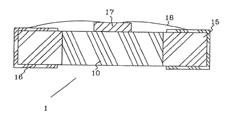
Figure 1 is a side-on sectioned view of a known capsule, minus
its cover member. The capsule 1 includes a flange 10, an
electrically insulating substrate 15, two electrical
CA 02336936 2001-O1-08
WO 00/03435 PCT/SE99/01193
connections 16, and a high frequency transistor chip 17 with
associated connection conductors 18. The flange 10 is produced
from an electrically conductive material whose coefficient of
linear expansion is adapted to the material in the electrically
5 insulating substrate 15. Although not shown, the capsule also
includes a cover member.,
Figure 2 shows the known capsule of Fig. 1 from above. It will
be evident from this perspective view that the electrically
insulating substrate 15 is arranged around the high frequency
transistor chip 17 in a frame-like configuration. It will also
be seen that the flange includes a pair of holes 20. These
holes are used to connect the flange 10 to a cooler by means of
a pair of screws or rivets
Figure 3 is a side-on sectioned view of an inventive capsule
minus its cover member. In this embodiment, the electrically
insulating substrates 15 are accommodated in two recesses on
the side edges of the flange 10. As apparent from Fig. 3, the
substrates 15 may have' the same height as the flange 10 to
which they are connected. The electrically insulating
substrates of the Fig. 3 embodiment are provided with
electrical connections 16 in the form of a metallisation from
one upper side, around the side edge and on an underside, so as
to obtain an electrical connection of low inductance between
the upper side and the under side of the capsule.
Figure 4 is a side view of the embodiment shown in Fig. 3.
Figure 5 shows the embodiment of Fig. 3 and Fig. 4 from above.
It will be evident from Figs. 4 and 5 that a gap has been left
between the metallisation and the flange 10, so as to avoid
contact therebetween. The electrically insulating substrates
CA 02336936 2001-O1-08
WO 00/03435 PCT/SE99/01193
6
can be metallised, by printing ? in a manner which is well
known to those skilled in this art and which will not therefore
be described in detail.
Figure 6 shows another embodiment an inventive capsule from
above, minus its cover member. In this embodiment, the
electrically insulatin<3 substrates have been arranged along the
full extension of the side edges of the flange instead of in
said recesses. As evident from Fig. 5, the metallisation that
forms the electrical connections on the substrates may be
somewhat incomplete, in other words the surfaces need not be
fully covered. However, the metallisation may not come into
contact with the flange 10.
Figure 7 is a side=on sectioned view of another embodiment of
an inventive capsule minus its cover member. In this
embodiment, the electrically insulating substrate 15 and the
edge of the flange .to which the substrate shall be connected is
modified with the intention of simplifying manufacture. In the
Fig. 7 embodiment, the connecting surfaces of the flange 10 and
the substrate 15 have been adapted to one another in step-like
configuration. This simplifies joining of the flange to the
substrate and allows~tr~e underside to be flat.
A possibility of improving the performance of the capsule lies
in placing so-called vias 25 through the electrically
insulating substrate 15 in accordance with Figure 8. Such vias
will reduce a series inductance in the electrical connections.
The flange may include a number of screw holes 20 or apertures
for mounting a circuit board or a cooler. However, the flange
CA 02336936 2001-O1-08
WO 00103435 PCT/SE99/01193
7
may alternatively be soldered to a circuit board, therewith
obviating the need for acrew holes.
Each electrically insulating substrate may include one or more
electrical connections 16.
Copper, copper-diamond -composite, copper-molybdenum-copper -
composite, copper-tungsten-copper -composite are examples of
materials that have good thermal conductivity and are
conceivably suitable as flange material.
It will be understood that the invention is not limited to the
described and exemplifying embodiments thereof and that
modifications can be made within the scope of the following
claims.