Note: Descriptions are shown in the official language in which they were submitted.
CA 02337471 2001-02-22
RESISTOR COMPONEN°T WITH ~'IULTIPLE LAYERS OF RESISTIVE
MATERIAL
Field of tloe Invention
The present invention relates to niulti-layer printed circuit boards and, more
particularly, to a resistive component usable in forming boards with embedded
resistive layers.
Back~,round of the Invention
A basic component of a printed circuit board is a dielectric layer having a
sheet
of copper foil bonded thereto. Through a subtractive process that includes one
or
more etching steps, portions of the copper foil are etched away to leave a
distinct
pattern of conductive lines and formed elements on the surface of the
dielectric layer.
Multi-layer printed circuit boards are formed by stacking and joining two or
more of
the aforementioned dielectric layers having printed circuits thereon. Many
printed
circuit boards include conductive layers containing patterned components that
perforce
like specific, discreet components. One such discreet component is a resistive
element
formed from a resistor foil. A resistor foil is basically a copper foil having
a thin layer
of resistive material, typically a metal or metal alloy deposited onto one
surface
thereof. The resistor foil is attached to a dielectric substrate with the
resistive material
adhered to the dielectric substrate. Using conventionally known masking and
etching
techniques, the copper foil and resistive material are etched away to produce
a trace
line of copper with the resistive material therebelow on the surface of the
dielectric. A
section of the copper layer is removed leaving only the resistive material on
the
surface connecting the two separated ends of the copper. Because the material
forming the resistive layer typically has a conductivity less than copper, it
essentially
acts as a resistor between the separated ends of the copper trace Lines. The
thickness
and width of the resistive layer, as well as the length of the resistive layer
disposed
between the ends of the copper traces, affect the resistance of the resistive
element so
formed.
The present invention represents an improvement over resistor foils known
heretofore and provides a resistor (oil having multiple layers of resistive
material on a
copper layer, thereby facilitating the formation of a variety of different
resistive
elements having a variety of resistance values.
CA 02337471 2001-02-22
2
Summary of the Invention
Ln accordance with a preferred embodiment of the present invention, there is
provided a resistor foil, comprised of a copper layer having a first side and
a second
side. A tiecoat metal layer having a thickness of between 5 ~ and 70 ~ is
provided on
the first side of the copper layer. A Iirst layer of a first resistor metal
having a
thickness of between 100 ~ and 500 A is on the tiecoat metal layer, and a
second layer
of a second resistor metal having a thicktvess of between 100 ~ and 500 ~ is
on the
first layer of the first resistor metal. The first resistor metal has a
resistance different
from the second resistor metal.
lp In accordance with another embodiment of the present invention, there is
provided a method of forming a resistive element on a printed circuit board,
comprising the steps of:
a) adhering a resistor foil to a dielectric substrate, the resistor foil
comprised of:
a copper layer havi~~g a first side and a second side;
a tiecoat metal layer having a thickness of between 5 ~ and 70
~ on the first side of the copper layer;
a first layer of a first resistor metal on the tiecoat metal layer;
and
a second layer of a second resistor metal on the first layer of the
first resistor metal, the first resistor metal having a resistance different
from the second
resistor metal, the resistor foil adhered to the substrate with the second
layer of the
second resistor metal facing the dielectric substrate;
b) forming a circuit trace line on the dielectric substrate from the
resistor foil; and
c) removing a portion of the copper layer and the tiecoat metal
layer from the circuit trace line to define a section of the circuit trace
line comprised of
the first and second layer of resistor metals.
These and other objects will become apparent from the following description
of a preferred embodiment taken together with the accompanying drawings and
the
appended claims.
CA 02337471 2001-02-22
3
Brief Descri ~tion of the Drawings
The invention may take physical form in certain parts and arrangement of
parts, a preferred embodiment of which will be described in detail in the
specification
and illustrated in the accompanying drawings which form a part hereof, and
wherein:
FIG. 1 is an enlarged, cross-sectional view of a resistor foil illustrating a
preferred embodiment of the present invention;
FIG. 2 is an enlarged, cross-sectional view of a resistor foil illustrating an
alternate embodiment of the present invention;
FLG. 3 is a cross-sectional view showing the resistor foils shown in FIG. 2
l0 attached to a dielectric substrate;
FIG. 4 is a perspective view of a resistive element formed from a resistor
foil
shown in FIG. 2;
FIG. 4A is a schematic, electrical representation of the resistive element
shown
ita FIG. 4;
FIG. 5 is a partially sectioned, side elevational view of another resistive
element shown in FIG. 2;
FIG. SA is a schematic, electrical representation of the resistive element
shown
in FIG. 5;
FIG. 6 is a partially sectioned, side elevational view of a still further type
of
resistive element formed using the resistor foil shown in FIG. 2;
FIG. 6A is a schematic, electrical representation of the resistive element
shown
Iil FIG. C7;
FIG. 7 is a cross-sectional view of a resistive element formed from a resistor
foil having three layers of resistive material thereon, illustrating another
embodiment
of the present invention;
FIG. 7A is a schematic, electrical representation of the resistive element
shown
in FIG. 7; and
FIG. 8 is a perspective view of a resistive element formed from the resistor
foil
shown in FIG. 2, illustrating another embodiment of tile present invention.
Detailed Description ofPrefeured Embodiment
The present invention relates to a resistor foil for use in forming embedded
resistive elements in printed circuit boards. Broadly stated, the resistor
foil is formed
of a resistive copper foil having two or more layers of resistive material
applied
CA 02337471 2001-02-22
4
thereto. The resistive materials are preferably formed of metal. As used
herein, the
term "metal" refers to metals and alloys capable of vacuum deposition by the
methods
discussed herein.
The copper foils used with this invention can be made using one of two
S techniques. Wrought or rolled copper foil is produced by mechanically
reducing the
thickness of a copper or copper alloy strip or ingot by a process such as
rolling.
Electrodeposited foil is produced by electrolytically depositing from solution
copper
ions on a rotating cathode drum and then peeling the deposited foil from the
cathode.
Electrodeposited copper foils find advantageous application with this
invention.
1 () The copper foils typically have nominal thicknesses ranging from about
0.0002
inch to about 0.02 inch. Copper foil thickness is sometimes expressed in terms
of
weight and typically the foils of the present invention have weights or
thicknesses
ranging from about '/8 to about 14 ounces per square foot (oz/ftZ). Especially
useful
copper foils are those having weights of !'3, '/Z, 1 or 2 oz/ftz.
15 Electrodeposited copper foils have a smooth or shiny (drum) side and a
rough
or matte (copper deposit growth front) side. The side or sides of the foil, to
which the
layer applied by the inventive process overlies, can be a "standard-profile
surface,"
low~profile surface" or "very-low-profile surface." Useful embodiments involve
the
use of foils with low-profile surfaces and very low-profile surfaces. The teen
20 "standard-profile surface" is used herein to refer to a foil surface having
a R"" (1PC-
MF-150F) of greater than 10.2p. The term "low-profile surface" refers to a
foil
surface having a R"" (1PC-MF-150F) of less than 10.2fr. The term "very-low-
profile
surface" refers to a foil surface having a R,", (IPC-MF-150F) of less than
S.llr. Rt",
(IPC-MF-150F) is the mean of the maximum peak-to-valley vertical measurements
2~ from each of five consecutive sampling measurements, and can be measured
using a
SURTRONIC~ 3 proClometer marketed by Rank Taylor° I-Iobson, Ltd.,
Leicester,
England.
The present invention finds advantageous application with copper foils of the
type heretofore described.
30 Refewing now to FIG. l, a resistor foil 10, illustrating a preferred
embodiment
of the present invention is shown in cross-section. Resistor foil 10 is
comprised of a
copper layer 12. A first layer 14 of a first resistive material is applied to
one side of
copper layer 12. Layer 14 is preferably funned of a metal or metal alloy that
is
CA 02337471 2001-02-22
deposited onto copper layer 12 by a deposition process such as vacuum
metalization,
electrodeposition, electroless deposition or combinations thereof. Layer 14 is
preferably applied to side 12a of copper layer 12 by an electrodeposition
process or
vacuum metalization. Layer 14 is formed of a metal having a resistivity
greater than
5 copper. Metals such as aluminum, zinc, nickel, nickel/chromium,
nickel/chromium/aluminum/silicon alloy, titanium, vanadium, chromium,
tantalum,
iron, manganese and alloys, oxides, nitrides and silicides thereof, as well as
any vapor
depositable metal or alloy, oxide, nitride and silicide whose electrical
resistivity~ is
greater than that of copper, find advantageous application in forming layer
14. In a
preferred embodiment, layer 14 is formed of a nickel/clu-
omium/aluminum/silicon
alloy. As layer 14 will ultimately be used to form a resistive element, the
thickness of
layer 14 will be based upon the resistivity of the metal forming layer 14 as
well as the
desired resistance of the resistive element to be forn~ed. In this respect,
layer 14 may
have a thickness of between 100 ~ and 500 t~, and more preferably between 100
~.
and 350 ~.
A second layer 16 of a second resistive material is applied onto layer 14.
Layer 16 is preferably fornled of a material different from that forming layer
14. The
material forming layer 16 preferably has a resistivity different from the
material
forming layer 14, wherein layer 16 has a resistance different from layer 14.
Layer 16 may be fornied from any of the same materials identified above i.e.,
aluminum, zinc, nickel, nickel/chrornium, nickel/chromium/aluminum/silicon
alloy,
titanium, vanadium, chromium, tantalum, iron, manganese and alloys, oxides,
nitrides
and silicides thereof, as well as any vapor depositable metal or alloy, oxide,
nitride and
silicide whose electrical resistivity is greater than that of copper, subject
to layer 16
having a resistance different from layer 14. In preferred embodiments, second
layer
16 is formed of compounds of tantalum and oxygen, e.g., Ta20;, compounds of
tantalum and nitrogen, e.g., ~faZN and TaNz, or compounds of chromium and
silicon,
e.g., CrSi.
Layer 16 is preferably applied by a deposition process such as vacuum
metalization, electrodeposition, electroless deposition or combinations
thereof. Layer
16 is preferably applied to layer 14 by an electrodeposition process or vacuum
metalization.
CA 02337471 2001-02-22
6
As with layer 14, the thickness of layer 16 will be based upon the desired
resistance of layer 16 and the resistance element to be formed, as well as on
the
material forming layer 16. In this respect, layer 16 may have a thickness of
between
100 E~ and 500 ~, and more preferably between 100 ~. and 350 ~.
S Referring now to FIG. 3, a resistor foil 20, illustrating an alternate
embodiment
of the present invention is shown. Resistor foil 20 is similar to resistor
foil 10, and
like elements are designated with like reference numbers. Resistor foil 20
differs from
resistor foil 10 in that a tiecoat layer, designated 18, is disposed between
copper layer
12 and first layer 14. 'fiecoat layer 18 is provided as an adhesion promoting
layer to
improve the adhesion of layer 14 to copper layer 12.
Tiecoat 18 may be formed of the following metals: nickel, palladium, titanium,
tantalum, aluminum, iron, vanadium, clwomium, chromium-based alloys and nickel-
based alloys. A metal tiecoat layer 18 is applied to a clean surface of the
copper. In a
preferred embodiment, tiecoat layer 18 is comprised of chromium. The chromium
tiecoat may be applied by a vacuum iieposition process such as sputtering, e-
beam
deposition or thermal evaporation. ~I'iecoat 18 has a thickness greater than 5
~..
Preferably, the thickness of tiecoat 18 is between 5 ~ and 70 ~, and more
preferably,
between about 10 t~ and about 20 ~.
Referring now to the use of resistor foil 10 or resistor foil 20 in forming a
resistive element, FIG. 3 shows resistor foil 20 adhered to a dielectric
substrate 30. As
will be appreciated from a further reading of the specification, the following
discussion would also apply if resistor foil 10 is used. Resistor foil 20 may
be secured
to dielectric substrate 30 using an adhesive (not shown), or adhered to
dielectric
substrate 30 by a lamination process, wherein dielectric substrate 30 is cured
with
resistor foil 20 attached thereto. Methods of securing a resistor foil, such
as foils 10
and 20 are conventionally known, and the particular method used in and of
itself is not
critical to the present invention.
Resistor foil 20 is attached to dielectric substrate 30 with second layer 16
closest to, and facing, substrate 30 (as shown in FIG. 3), and with copper
layer 12
exposed. Using conventionally known processes of masking and etching, unwanted
areas of resistor foil 20 are etched away to leave a circuit pattern (not
shown) on the
surface of dielectric substrate 30.
CA 02337471 2001-02-22
7
FIG. 4 is a perspective view of a portion of a circuit showing a trace line 40
on
substrate 30. A section, designated "X," of copper layer 12 is removed from
trace line
40, by conventionally known masking and etching techniques, to leave only
first and
second layers 14, 16 of first and second resistor materials connecting the
spaced-apart
ends of copper layer 12. In other words, section X essentially forms a
resistive
element between the spaced-apart ends of copper layer 12 of trace line 40. Any
current flow through trace line 40 must necessarily flow tl' -ough first and
second
layers 14, 16 of section X. Since first layer 14 has a different resistance
than second
layer 16, the total resistance of section X is a function of both layers 14,
16.
FIG. 4A is an electrical, schematic representation of the resistance of
section
X. The resistive element shown in FIG. 4 is the equivalent of two resistors
R,4, Rib in
parallel, where Ri4 is the resistance of first layer 14 in section X and Rib
is the
resistance of second layer 16 in section X. The total resistance, RTOTAL~ of
the
resistive element shown in FIG. 4 is determined by the following equation:
(Rta) (R«)
TOTAL =
Ko + Km
FIG. 5 shows a variation to trace element 40, as shown in FIG. 4, that
produces
a different resistive element. In the embodiment shown in FIG. S, first layer
14 is also
etched away in section X (by conventional masking and etching techniques),
leaving
only second layer 16 in section X. The resistance of the element shown in FIG.
5 is a
function of resistance R,6 of second layer 16 in section X. The resulting
resistive
element is equivalent to that schematically illustrated in FIG. SA. FIGS. 4-SA
thus
show how two different resistive elements may be formed from the same resistor
foil
10 by merely changing the number of layers removed, i.e., etched away, from
trace
line 40.
FIGS. 6 and 6A show still another embodiment of a resistive element that may
be formed from resistor foil 10. In the embodiment shown in FLG. 6, resistor
foil 10
has been masked and etched to form a trace line (shown in cross-section in
FIG. 6) and
the trace live masked and etched to form a resistive element having a central
section
"X" and two sections "Y" adjacent thereto. In section X, only second layer 16
remains. In sections Y, both first arid second layers 14 and 16 remain.
CA 02337471 2001-02-22
8
The resistance of the resultant stn~cture is shown in FIG. 6A, wherein the
resistance of sections Y are equivalent to two resistors R,4Y and R,~Y in
parallel,
wherein R~av is the resistance of first layer 14 in section Y and R~6Y is the
resistance
of second layer 16 in section Y. T'he resistance of section X is R,~X which is
the
resistance of second layer 16 in section X. The total resistance of the
structure shown
in FIGS. 6 and 6A is the sum of the resistances of each section.
The resistive elements heretofore described were formed with a resistor foil
10
having two layers of resistive materials tinereon, i.e., first layer 14 and
second layer 16.
FIG. 7 shows a cross-sectional view of a resistive element formed from a
resistor foil
l0 1 10 having three layers of resistor material thereon. Resistor foil 110
has a copper
layer 112, a first layer 114 of a first resistive material, a second layer l
15 of a second
resistive material and a third layer 1 l6 of a third resistive material. Each
resistive
material has a different resistivity such that each Layer 114, 115 and 116 has
a different
resistance value. Resistor foil 110 is masked and etched to produce a central
zone "X"
1 S comprised of layer 116, intermediate sections "Y" comprised of layers 115
and 116
and outer sections "Z" comprised of layers 114, 1 15 and 116. As shown in FIG.
7A,
and like the structures previously discussed, the resistance of the stmcture
shown in
FIG. 7 is the sum of resistance of each of sections X, Y and Z, and the
resistance of
sections Y and Z are determined by the respective resistances of layers 114,
115 and
20 116 in parallel. FIG. 7 thus illustrates that a resistor foil having more
than two
resistive layers may be formed and a variety of different resistor values can
be created.
Heretofore, single trace lines having resistive elements formed therein have
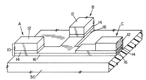
been described. FIG. 8 illustrates how a circuit having a junction of three
branches,
designated A, B and C, can be formed from resistor foil 10. FIG. 8 illustrates
how
25 multiple branch trace lines having one or more branches with different
resistances may
be formed.
The foregoing description discloses specific embodiments of the present
invention. These embodiments are described for purposes of illustration only.
Numerous alterations and modifications may be practiced by those skilled in
the ail
30 without departing from the spirit and scope of the invention. It is
intended that all
such modifications and alterations be included insofar as they come within the
scope
of the invention as claimed or the equivalents thereof.