Note: Descriptions are shown in the official language in which they were submitted.
CA 02337601 2001-05-29
A Kolsrud 9-8 1
A HIGH-POWER SELECTIVE SIGNAL ATTENUATOR AND METHOD
O:E' ATTENUATION
Bac round of the Invention
1. Field of the Invention
The present invention; relates to signal attenuation; and more
particularly, a high power selective signal attenuator and method of
attenuation.
2. Description of Related Ao:~t:
Analog-to-digital converters (ADCs) have a dynamic range of
operation. The dynamic range is defined as the range from a
minimum signal amplitude to a maximum signal amplitude (i.e.,
between a minimum and maximum power level). Analog signals
having amplitudes within the dynamic range of an ADC will be
converted from analog to digital.
Analog signals having; amplitudes below the minimum power
level of the dynamic range will not undergo conversion, while analog
signals having amplitudes greater than the maximum power level of
the dynamic range will overload or saturate the ADC. More
specifically, the ADC will clip the amplitude of an analog signal having
an amplitude greater than the maximum power level of the ADC's
dynamic range. Clipping the amplitude of the analog signal causes
harmonics which distort and corrupt the whole spectrum such that
most signals are virtually lost. Consequently, such ADCs are
unsuitable for many of today's communication needs.
SUMMARY OF THE INVENTION
The high.-power selective signal attenuator according to the
present invention isolates high-power signals in the received analog
CA 02337601 2001-05-29
A Kolsrud 9-8 2
signal spectrum. The isolated high-power signals are then
recombined ~~ith the received analog signals such that the high-power
signals are substantially canceled from the received analog signals.
The isolation of the high-power signals is accomplished by coupling
the received analog signals onto a feed forward pathway, and
attenuating the coupled signals so that high-power signals fall within
the dynamic range of an ADC receiving the attenuator's output.
Because the ADC performs the analog-to-digital conversion operation
on signals falling within its dynamic range, the output of the ADC
substantially represents the high-power signals in the received
signals. The digital signals a.re then digital-to-analog converted and
amplified by an amplifier, which compensates for the attenuation
caused by at least the attc~nuator. The resulting signals are then
combined 180E out of phase with the received analog signals so that
the high-power signals are substantially canceled from the received
analog signals..
The attenuation performed by the attenuator in the high-power
selective signal attenuator i;s dynamically controlled by monitoring the
output of a primary ADC receiving the output of the high-power
selective signal attenuator. As the primary ADC approaches
saturation, the attenuation level is increased. As the primary ADC
falls further from saturation, the attenuation level is decreased. In
this way, the maximum amount of information can be converted by
the primary ADC without placing the primary ADC in saturation.
BRIEF DESCRIPTION OF THE DRAWINGS
The present invention will become more sully understood from
the detailed description given hereinbelow and the accompanying
CA 02337601 2001-05-29
A Kolsrud 9-8 3
drawings which are given by way of illustration only, wherein like
reference numerals designate corresponding parts in the various
drawings, and wherein:
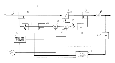
Fig. 1 illustrates an embodiment of a high-power selective
signal attenuator according to the present invention;
Fig. 2A illustrates thf: coupled signals prior to attenuation; and
Fig. 2B illustrates t:he~ coupled signals after attenuation.
DETAILED DESCRIPTION OF THE PREFERRED EMBODIMENTS
Fig. 1 illustrates a high-power selective signal attenuator
according to an embodiment of the present invention. As shown, the
high-power selective signal ;~ttenuator 2 selectively attenuates analog
main signals received at an input, and supplies the resulting
attenuated main signals to the input of a primary ADC 28. The high-
power selective signal attenuator 2 operates based on a clock signal
received from a converter clock 4 and control inputs received from
control circuitry 32. The control circuitry 32 generates the control
inputs based on processing performed by a signal processor 30 on the
output of the primary AD(: :78.
As further shown in F'ig. 1, the high-power selective signal
attenuator 2 includea a prinnary pathway 6 and a feed forward
pathway 8. The primary pathway 6 includes a delay 26 between a
first coupler 10 and a second coupler 24. The first coupler 10 couples
the main signals on the primary pathway 6 onto the feed forward
pathway 8. An attenuator 12 attenuates the signals on the feed
forward pathway 8, and a secondary ADC 16 analog-to-digital
converts the output of the attenuator 12. A digital-to-analog convertor
(DAC) 18 converts the output of the secondary ADC 16 to analog, and
CA 02337601 2001-05-29
A Kolsrud 9-8 4
an amplifier 20 amplifies the output of the DAC 18. The second
coupler 24 couples the signals on the feed forward pathway 8 back
onto the primary pathway Ei.
As further shown in Fig. l , the high-power selective signal
attenuator 2 optionally includes a dither signal generator 34, a third
coupler 14, and a dither signal remover 22. The dither signal
generator 34 generates a low frequency dither signal at an amplitude
controlled by the control circuitry 32, and the dither signal is coupled
onto the feed forward pathway 8 by the third coupler 14 disposed after
the attenuator 12. The dither signal remover 22 removes the dither
signal and is disposed after t:he amplifier 20. The attenuator 12, the
amplifier 20, the delay 26 anal the dither signal generator 34 operate
based on control inputs received from the control circuitry 32.
Furthermore, the secondary ADC 16 and the DAC 18 operate
15. according to a clock signal received from the converter clock 4.
The operation of the high-power selective signal attenuator
according to the embodiment of the present invention illustrated in
Fig. 1 will now be described with reference to Fig. 1 and Figs. 2A-2B.
The high-power selective signal attenuator 2 attenuates analog
signals having amplitudes greater than the maximum power level of
the dynamic range of the primary ADC 28. To do this, analog signals
exceeding the maximum power level are isolated by circuitry in the
feed forward pathway 8 of the high-power selective signal attenuator
2, amplitude adjusted, and then combined with the main signals on
the primary pathway 6 to selectively cancel portions of these high
amplitude (i.e., high power) signals from the main signals.
Specifically, the first coupler 10 couples the analog main signals
CA 02337601 2001-05-29
A Kolsrud 9-8 5
from the primary pathway 6 onto the secondary pathway 8. The
attenuator 12 attenuates the coupled signals to an amplitude less
than a power-level threshold established by the control circuitry 32.
As discussed in more detail below, the control circuitry 32 adjusts the
power level threshold of the att:enuator 12 such that the amplitudes of
the coupled signals exceeding the maximum power level in the
dynamic range of the secondary ADC 16 fall within the dynamic range
of the secondary ADC 16. 1'damely, the power-level threshold is less
than or equal t=o the maximum power level. As a result of this
10. attenuation operation, some: signals which fell within the dynamic
range of the secondary ADC. 16 prior to attenuation, will no longer fall
within the dynamic range o:f the secondary ADC 16.
The attenuation operation is clearly illustrated in Figs. 2A and
2B. Fig. 2A illustrates the amplitude of coupled signals at
15~ frequencies W :l and W2 prior to attenuation. As shown, the amplitude
of the coupled signal at frequency W 1 falls within the dynamic range
of the secondary ADC 16, while the amplitude of the coupled signal at
frequency W2 exceeds the dynamic range. Fig. 2B illustrates the
amplitudes of the coupled signals at frequencies W 1 and W2 after
2C~ attenuation. As shown in F'ig. 2B, the amplitude of the coupled
signal at frequency W 1 now i:alls below the dynamic range of the
secondary ADC 16, while th.e amplitude of the coupled signal at
frequency W2 now lies within the dynamic range of the secondary
ADC 16.
25. The sect>ndary ADC 1b converts the analog coupled signals into
digital signals. Specifically, only those frequencies having amplitudes
falling within the dynamic range of the ADC will undergo conversion.
CA 02337601 2001-05-29
A Kolsrud 9-8
As such, frequency W2 will be converted, while frequency W 1 will not;
hence, the information pertaining to frequency W 1 is lost.
Digital signals output by the secondary ADC 16 are converted
back to analog by the DAC 18, and the amplitudes of the analog
signals output from the DAC: 1.8 are amplified by the amplifier 20. The
gain of the amplifier 20 is controlled by the control circuitry 32 so that
the amplitude of the signals coupled back onto the primary pathway 6
by the second coupler 24 are' substantially equal to the amplitudes of
the same signals prior to being coupled onto the feed forward pathway
8 by the first coupler 10. Namely, the amplifier 20 cancels out
attenuation of the main signals caused by the first coupler 10, the
attenuator 12, the third coupler 14 (if present), the secondary ADC 16,
the DAC 18, the dither signal remover 22 (if present) and the second
coupler 24. Because the power-level threshold of the attenuator 12
dynamically changes, the control circuitry 32 dynamically changes the
gain of the amplifier 20 in association therewith.
As discussed above, the: second coupler 24 then couples the
output of the amplifier 20 back onto the primary pathway 6 such that
the signals coupled from the feed forward pathway 8 onto the primary
pathway 6 are 180E out of phase with the main signals on the
primary pathway 6. Depending upon phase differences generated by
the components on the feed i:orward pathway 8, (including the first
and second couplers 10 and 2,4), the delay 26 delays the main signal
to establish a phase difference of 180E between the signals being
coupled onto the primary pal:hway 6 by the second coupler 24 and the
main signals output from the delay 26 on the primary pathway 6.
Because t:he signals being coupled onto the primary pathway 6
CA 02337601 2001-05-29
A Kolsrud 9-8 7
mostly include the high power signals, v~~hich are 180E out of phase
with the high power signals in the main signals, these high-power
signals are substantially canceled from the main signals.
Next, the optional dither signal generation will be described
followed by a description of the dynamic control of the high-power
selective signal attenuator 2 by the control circuitry 32.
The use of a dither signal to improve the operation of ADC is
well-known in the art. Ther~°fore, the conceptual underpinning behind
the use of dither signals will not be described. Instead, only the
insertion and removal of the dit:her signal in the high-power selective-
signal attenuator 2 will be described. As shown in Fig. 1, the dither
signal generator 34 generates a low frequency dither signal at an
amplitude controlled by the control circuitry 32 as described below,
and the dither signal is coupled onto the feed forward pathway 8 by a
third coupler 14. The addition of the dither signal influences and
improves the operation of the secondary ADC 16. After the analog
signal output from the DAC 18 is amplified by the amplifier 20, the
dither signal remover 22 removes the dither signal from the feed
forward pathway 8. In this manner, the operation of the secondary
ADC 16 is improved.
While the power-level threshold of the attenuator 12 and the
gain of the amplifier 20 could be set to fixed values, the main signals
for conversion from analog-to-digital by the primary ADC 28 change
over time, and could eventually cause saturation of the primary ADC
28 absent some type of dynamic control of the attenuation operation
performed by the high-power selection signal attenuator 2. By
monitoring the output of the primary ADC 28, it is determined
CA 02337601 2001-05-29
A Kolsrud 9-8 g
whether or not the output of the high-power selective signal
attenuator 2 is approaching; levels which would cause saturation of
the primary ADC 28, or alternatively, fall to such levels that the
primary ADC 28 is failing to convert a substantial amount of the
information in the main signals.
To dynamically control the operation of the high-power selective
signal attenuator 2, a signal processor 30 performs a frequency
analysis on the output of the primary ADC 28. For instance, the
signal processor 30 performs a fast Fourier transform (FFT) on the
output of the primary ADC 28 and sums the power in the various
frequency bins of the FFT tc> obtain a total power. The control
circuitry 32 includes an empirically determined lookup table to map
the total power to a desired power-level threshold for the attenuator
12, gain for the amplifier 20~, and optionally, amplitude of the dither
signal. One skilled in the art will readily appreciate from the foregoing
example that many different types of analysis can be performed on the
output of the primary ADC: :Z8 to determine whether or not the
primary ADC 28 is approaching saturation or, in the opposite, so far
from saturation that the main signals can be amplified to increase the
amount of information falling within the dynamic range of the primary
ADC 28.
Besides the power-level threshold of the attenuator 12, the delay
through the delay 26 affecas, hove well high power signals are cancelled
from the main signals. The l=ime it takes to process signals through
the feed forward pathway 8 varies with the frequency of the signals
being processed. Accordingly, the phase difference between the signals
coupled onto the primary pathway 6 by the second coupler 24 and the
CA 02337601 2001-05-29
A Kolsrud 9-8 9
signals on the primary pathway 6 output by the delay 26 can deviate
from 180 degrees arid cause imperfect cancellation. This can result in
the primary ADC 28 approaching saturation.
Therefore, in addition t:o dynamic control of the attenuator 12
and the amplifier 20, the control circuitry 32 dynamically controls the
delay through the delay 26. In one embodiment, the control circuitry
32 receives the FFT performed by the signal processor 30, and
identifies a frequency bin having a power level exceeding a
predetermined threshold indicating that the primary ADC 28 is
approaching saturation. Thf: control circuitry 32 then incrementally
increases the delay through t:he delay 26, and monitors the power for
the identified frequency bin after each increment. If the power in the
identified frequency bin dc:c:reases, the control circuitry 32 continues
incrementing the delay through the delay 26 until there is no longer a
decrease in the power of the identified frequency bin. If, instead of a
decrease, incrementing the delay through the delay 26 causes an
increase in the power of the identified frequency bin, the control
circuitry 32 begins incrementally decreasing the delay through the
delay 26. If the power in the identified frequency bin decreases, the
control circuitry 32 continues decreasing the delay through the delay
26 until there is no longer a decrease in the power of the identified
frequency bin. If decreasing the delay through the delay 26 also fails
to cause a decrease in the power of the identified frequency bin, the
control circuitry 32 restores the delay through the delay 26 to the
initial value prior to attempt:ing dynamic control.
A similar operation can also be performed with respect to the
gain of the amplifier 20 to account for inaccuracies in the correlation
CA 02337601 2001-05-29
A Kolsrud 9-8 10
between the gain of the amplifier and the attenuation caused by the
other elements in the feed forward path~~ay 8.
The control circuitry 3'~ can perform dynamic control of the
attenuator 12 (and in conjunction, the amplifier 20), the delay 26, and
the amplifier 20 sequentially, in parallel, at different time intervals,
etc. It is expected that each individual designer will make use of the
dynamic control functions in different ways to optimize the
performance of the system being designed.
As demonstrated above, the high-power selective signal
attenuator according to the present invention attenuates high-power
signals so that an ADC connected thereto will not be placed in
saturation. Additionally, the high-power selective signal attenuator is
dynamically controlled so that the maximum amount of information is
transferred to the ADC without placing the ADC in saturation.
The invention being thus described, it will be obvious that the
same may be varied in many ways. Such variations are not to be
regarded as a departure from the spirit and scope of the invention,
and all such modifications are intended to be included within the
scope of the following claims.