Note: Descriptions are shown in the official language in which they were submitted.
CA 02337714 2001-02-22
Kaminski-Kolsrud 7-i 1
RECEIVER SYSTEM USING ANALOG TO DIGITAL CONVERSION AT
RADIO FREQUENCY AND METHOD
BACKGROUND OF THE INVENTION
1. Field of The Invention
This invention relates to a wireless communications and, more particularly, to
a receiver architecture in a wireless communications system using analog to
digital
conversion at radio frequency (RF).
2. Description of Related Art
1o The service area of a wireless communications system is partitioned into
connected service domains known as cells, where wireless units communicate via
radio links with a base station (BS) serving the cell. The base station is
coupled to a
land network, for example through a Mobile Switching Center (MSC) which is
connected to a plurality of base stations dispersed throughout the service
area. In the
wireless communications industry, a service provider is often granted two or
more
non-contiguous or segregated frequency bands to be used for the wireless
transmission and reception of RF communications el~annels: 'For example, in
the
United States, a base station for an "A" band provider for cellular
communications
receives frequency channels within the A (825-835 MHz), A' (845-846.5 MHz) and
2o A" (824-825MHz) bands, and the wireless units receive frequency channels
within
the A (870-880 MHz), A' (890-891.5 MHz) and A" (869-870MHz) bands. A base
station for a B band provider receives frequency channels within the B (835-
845MHz)
and B'(846.5-849 MHz) frequency bands, and the wireless units receive
frequency
channels within the B (880-890MHz) and B'(891.5-894 MHz) frequency bands.
Additionally, a base station for a Personal Communications Systems (PCS)
provider
may receive frequency channels from wireless units on one or more PCS bands
(1850MHz-1910MHz), and the wireless units receive frequency channels on one or
more PCS bands (1930-1990 MHz).
In order to reduce system hardware costs, a service provider would want to
3o use a common receiver for the simultaneous reception and processing of
signals
CA 02337714 2001-02-22
Kaminski-Kolsrud 7-i i 2
within the non-contiguous frequency bands. In a typical receiver architecture,
a
down-conversion stage for each frequency band is typically used to down-
convert and
to manipulate the placement of each frequency band at intermediate frequencies
(IF)
such that the frequency bands of the modulated analog signals are converted to
a
corresponding IF frequency spectrum and can be sampled at a reduced sampling
rate
by separate analog to digital (A/D) converters. To use a single A/D converter
to
digitize the modulated analog signals in the non-contiguous bands, a single
A/D
would have to sample at a high enough rate to encompass both frequency bands.
This
is an inefficient approach because the A/D converter is using bandwidth in
sampling
1 o unwanted frequencies in the gap between the frequency bands. To reduce the
frequency gap between non-contiguous frequency bands, a down-conversion stage
for
each of the frequency bands is used to down-convert and manipulate the
placement of
each frequency band at IF such that the bands are closer together to fit in a
smaller
Nyquist bandwidth. Another approach to improve the efficient use of the A/D
15 converter bandwidth involves down-converting both frequency bands such that
a
replica of one of the frequency bands is positioned in the frequency gap
between the
frequency bands.
When the IF spectrum is sampled by an A/D converter at a sampling rate
which is greater than or equal to twice the combined signal bandwidth, which
can be
2o referred to a the Nyquist sampling rate, the A!D input signal bandwidth
rotates or
folds periodically about itself at multiples of one-half the sampling
frequency. As
such, the signal bandwidth and mirror images of the signal bandwidth are
periodically
repeated at frequency intervals corresponding to the sampling rate of the A/D
converter. Each replica of the signal bandwidth can be referred to as a
Nyquist zone,
25 and the IF signal bandwidth folds back to the first Nyquist zone between
about OHz
and one-half the sampling frequency. The bandwidth of a Nyquist zone
corresponds
to the Nyquist bandwidth.
The periodicity of the spectral density in the digital domain is a basic
property
of sampled waveforms which can be predicted by determining the Fourier
transform
CA 02337714 2001-02-22
Kaminski-Kolsrud 7-~ i
of the time-sampled waveform. Generally, the A/D converter samples at at least
twice
the bandwidth of the composite frequency bands (i.e. the Nyquist sampling
rate) to
obtain a digital representation of the modulated analog IF signal.
Accordingly, the
sampling rate for the A/D converter is chosen such that the Nyquist bandwidth
encompasses the desired IF frequency bands. The higher the sampling rate, the
wider
is the Nyquist bandwidth. If the waveform is sampled at a rate less than twice
its
signal bandwidth (the Nyquist bandwidth), an undesirable overlapping between
the
adjacent periodic spectrums can occur - a well known phenomena known as
aliasing.
Accordingly, the sampling rate and the IF frequency are chosen such that the
Nyquist
to bandwidth encompasses the frequency band to be converted while reducing the
sampling rate of the A/D converter, enabling the use of lower sampling rate
A/D
converters with reduced cost. Accordingly, the wider the separation or
frequency gap
between the frequency bands, the current receiver architectures reach a point
where
the use of a single A/D is not viewed as practical or efficient.
15 If the frequency bands are far enough apart or if desired, a separate
antenna is
used for each segregated frequency band. In multiple antenna architectures
where
antennas are dedicated to different frequency bands, a separate branch is used
in
which a frequency conversion stage including a mixer and a local oscillator
(LO) are
used to down-convert the radio frequency (RF) analog signals to intermediate
2o frequencies (IF), and an A/D is typically used for each antenna path. The
above
receiver architectures do not take advantage of the potential bandwidths and
flexibility provided by the A/D converters in converting analog signals into
the digital
domain.
25 SUMMARY OF THE INVENTION
The present invention involves a receiver which receives analog signals at
radio frequency (RF), and the RF analog signals are converted into the digital
domain.
As such, the receiver does not require frequency conversion stages) prior to
analog to
digital conversion. For example, the receiver can comprise at least one
antennas)
CA 02337714 2004-10-19
4
which receives radio frequency (RF) analog signals at different frequency
bands. The
analog RF signals are provided to a single analog to digital (A/D) converter,
and the
A/D converter converts the analog RF signals at the different frequency bands
into
digital signals within the Nyquist bandwidth. By properly selecting the
sampling rate
of the AlD converter for the RF analog signals, the A/D converter can produce
replicas
of the different frequency bands of the analog signals in non-overlapping
portions of
the Nyquist bandwidth.
In accordance with one aspect of the present invention there is provided a
method of processing received signals, said method comprising: providing,
without
requiring frequency conversion or down-conversion to RF, analog signals at
different
RF bands on a plurality of channel branches; combining said analog signals at
said
different RF frequency bands on said plurality of branches; and digitally
converting
said analog signals at said different RF frequency bands at a selected
sampling rate to
produce digital signals at different frequency bands, said sampling rate
selected so that
said different frequency bands of said analog signals fold back to
substantially
non-overlapping portions of a Nyquist zone as said analog signals are
digitally
converted.
In accordance with one aspect of the present invention there is provided a
receiver, comprising: at least one antenna for receiving analog signals in
different radio
frequency (RF) frequency bands; a channel branch arrangement connected to said
at lease
one antenna for receiving analog signals and providing, without requiring
frequency
conversion or down-conversion to RF, analog signals onto a plurality of
channel
branches at different RF bands; a combining arrangement connected to said
plurality of
channel branches for combining said analog signals on said plurality of
channel
branches; and an analog to digital converter configured to receive and
digitally convert
said analog signals at said different RF bands to produce digital signals at
different
frequencies.
CA 02337714 2004-02-19
4a
BRIEF DESCRIPTION OF THE DRAWINGS
Other aspects and advantages of the present invention may become apparent
upon reading the following detailed description and upon reference to the
drawings in
which:
FIG. 1 shows a general block diagram of a receiver according to the principles
of the present invention;
FIG. 2 shows the different frequency bands at the A/D input frequencies and
the replicas of the analog signals in the different Nyquist zones which fold
back to the
first Nyquist zone in the digital domain;
FIG. 3 shows a general block diagram of an example embodiment of a multiple
band receiver according to principles of the present invention;
FIG. 4 shows the frequency bands at the A/D input frequencies and the replicas
of the frequency bands at the digital domain frequencies of the first Nyquist
zone for
the multiple band receiver of FIG. 3;
FIG. 5 shows a Nyquist zone frequency plan for an A/D converter using a
sampling rate of 61.44 MHz; and
FIG. 6 shows Nyquist zone channels with replicas of the frequency bands at
RF.
CA 02337714 2001-02-22 '
Kaminski-Kolsrud 7-11 5
DETAILED DESCRIPTION
Illustrative embodiments are described below of a receiver system using a
single analog to digital (A/D) converter to convert RF analog signals into the
digital
domain. The RF analog signals are digitally converted using a sampling rate
for the
A/D converter which produces a replica of the signal bandwidths) at RF in the
Nyquist bandwidth. As such, the receiver architecture according to the
principles of
the present invention does not require frequency conversion stage(s), which
comprise
mixers) and local oscillator(s), to down-convert the RF analog signals.
Furthermore,
by using a single A/D converter, the receiver provides time and/or phase
coherent
1o sampling of analog signals in different frequency bands) in certain
embodiments.
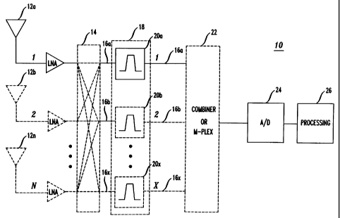
With particular reference to FIG. 1, a receiver 10 includes N antennas 12a-n
which receive analog signals over RF communications channels, where N>=1. The
antenna 12a could be a multiple frequency band antenna. A channel branch
distributor 14, such as an N-plexer filter or combiner array, combines and/or
separates
the received RF analog signals or portions thereof and provides the received
analog
signals into X channel branches 16a-x in a desired manner, where X>=l and can
but
need not be equal to N. For example, different channel branches 16a-x can
carry the
analog signals for corresponding RF frequency bands, the channel branches 16a-
x
can carry RF analog signals received by different antennas) or sets of
antennas,
2o and/or multiple channel branches having copies of the RF analog signals of
different
or contiguous frequency bands. In this embodiment, a filter arrangement 18
provides
at least two different RF frequency bands on at least one channel branch 16a-
x. For
example, the filter arrangement 18 can include a filter 20a-x on each channel
branch
16a-x which passes a frequency band on the respective channel branch 16a-x
while
attenuating other frequencies. Alternatively, depending on the embodiment, the
channel branch distributor 14 can simply include direct connections) from the
antennas) 12a-n to the filter arrangement 18, and the filter arrangement 18
can
include a filter 20a-x for each channel branch 16a-x.
CA 02337714 2001-02-22
Kaminski-Kolsrud 7-~ i 6
A combining arrangement 22 combines the RF analog signals on the channel
branches 16a-x in desired fashion. The resulting composite analog signal is
provided
with analog signals in different frequency bands to an analog to digital
converter 24
which digitizes the RF analog signals and provides the digitized signals to
digital
processing circuitry 26. Alternatively, depending on the embodiment, if the
receiver
has a single branch 16, the combining arrangement 22 is simply a connection
from
the antenna 12 through the filter 20 (if required) to the A/D converter 24.
A sampling rate for the A/D converter 24 is selected such that the frequency
bands of the RF analog signals on the channel branches 16a-x fold back to non-
10 overlapping portions of the first Nyquist zone which reflects the Nyquist
bandwidth
provided by the analog to digital (A/D) converter 24. The Nyquist sampling
rate for a
modulated analog signal, for example where an information signal is modulated
onto
a carrier signal, can be defined as being at least twice the highest frequency
component of the information signal regardless of the carrier frequency on
which the
information signal is modulated. The information, which can be voice, data,
video,
text and/or other information, is carried in the signal bandwidth. The highest
frequency component of the information signal is directly related to the
signal
bandwidth. Because the signal bandwidth is sampled at at least twice the
highest
frequency component of the information signal, the information signal can be
2o reproduced in the digital domain.
When the frequency spectrum is sampled by an A/D converter 24 at the
sampling rate of at least twice the combined signal bandwidth, which can be
referred
to as the Nyquist sampling rate, the signal bandwidth rotates or folds
periodically
about itself at frequency multiples or intervals ("Nyquist zones") of one-half
the
sampling frequency back to a first Nyquist zone in the digital domain from 0
Hz to
one-half the sampling rate. As such, a signal bandwidth and a mirror image of
the
signal bandwidth periodically repeats at frequency intervals corresponding to
the
sampling rate of the A/D converter. For example, a signal bandwidth in an odd-
numbered Nyquist zone will appear in the same relative position in odd
numbered
CA 02337714 2001-02-22
Kaminski-Kolsrud 7-11 7
Nyquist zones back to the first Nyquist zone yet appear as a minor image in
the even-
numbered Nyquist zones. Moreover, a signal bandwidth in an even-numbered
Nyquist zone appears as a mirror image in the odd-numbered Nyquist zones back
to
the first Nyquist zone while appearing in the same relative position in the
even-
numbered Nyquist zones. Therefore, replicas of the signal bandwidths) are
repeated
at intervals of one-half the sampling rate. The sampling rate for the A/D
converter is
chosen such that after the analog signals are digitized, the desired replica
frequency
bands occupy non-overlapping portions or-channels of the first Nyquist zone.
The
digital conversion effectively preserves the information being produced at a
rate of
less than or equal to one-half the sampling rate in the bandwidth of the first
Nyquist
zone. If the sampling rate is increased, the first Nyquist zone or Nyquist
bandwidth
becomes wider.
In this embodiment, a fast Fourier transform (FFT) of the digital signal
values
provides signals at frequency bands ("Nyquist zone channels") within one-half
the
sampling rate ("the first Nyquist zone") representing the converted analog
signals. If
the waveform is sampled at a rate less than twice its, signal bandwidth (the
Nyquist
bandwidth), an undesirable overlapping between the adjacent periodic spectrums
can
occur - a well known phenomena known as aliasing. Accordingly, the sampling
rate
is chosen to avoid loss of information due to aliasing.
2o For example, as shown in FIG. 2, in converting the analog signal at
different
RF bands into the digital domain, the A/D converter 24 processes the composite
analog signal into Nyquist zone channels 30a-x or bands in the first Nyquist
zone.
The Nyquist zone channels 30a-x in the digital domain correspond to the
different
frequency bands 28a-x of the RF analog signals. The digital signal processing
circuitry 26 can retrieve the digital signals from the Nyquist zone channels
of the first
Nyquist zone, because the different channels eventually end up in the first
Nyquist
zone after digitizing the analog input signals, for example using digital
filters, digital
combiners, digital detectors, digital demodulators, digital downconverters,
such as a
Digital Down Converter (DDC) with Numerical Controller Oscillator (NCO) to
CA 02337714 2001-02-22
Kaminski-Kolsrud 7-11 8
digitally down convert the data rate (which is referred to as decimation),
and/or other
digital processing. The DDC can tune to the respective frequencies for further
signal
processing. Therefore, the receiver 10 can use the bandwidth available in a
single
A/D to process the RF analog signals from different RF frequency bands.
As such, the receiver 10 according to the principles of the present invention
eliminates the need for a mixer/LO combination on any of the channel branches
16a-
x. A receiver 10 without a mixer/LO combination has many advantages. For
example, without a fixed local oscillator (LO) in the frequency conversion
stages, DC
power consumption is reduced, re-radiation of LO out of the antenna is
eliminated
which reduces the need for extra front-end filtering, filter requirements at
the IF are
eliminated, and no image band filters are required. Because a mixer is not
required,
spurious mixer products as well as intermodulation distortion produced by the
mixer
are removed, thereby improving the spurious free dynamic range. Additionally,
losses introduced by the mixer are removed which reduce the required channel
gain
and which improve the noise figure and the gain linearity. Furthermore, by
using a
single A/D converter, the receiver provides time and/or phase coherent
sampling of
analog signals in different frequency band(s). Different applications or
signal
processing schemes can benefit from such improved time and/or phase coherent
measurements.
Depending on the embodiment and due to the flexibility of the receiver
according to the principles of the present invention, the receiver can be
implemented
in different ways to use the potential bandwidth of an A/D converter 24. FIG.
3
shows an embodiment of a multiple band receiver 50 according to certain
principles
of the present invention which is used to receive communications signals in
the
cellular and the Personal Communications System (PCS) frequency bands. In the
United States, a base station for a "A" band cellular service provider
receives
frequency channels within the A (825-835MHz), A" (824-825MHz) and A' (845-
846.5 MHz) bands. A base station for a B band cellular service provider uses
the B
(835-845MHz) and B' (846.5-849MHz) frequency bands. In this example, a first
CA 02337714 2001-02-22
Kaminski-Kolsrud 7-11 9
antenna 12a receives the modulated analog signals within the entire cellular
base
station receive band (824-849 MHz), and a second antenna 12b receives the
modulated analog signals in the entire PCS base station receive band ( 1850-
1910
MHz).
In this embodiment, the RF analog signals from the antenna 12a are provided
to a first channel branch 16a, and the RF analog signals from the antenna 12b
are
provided to a second channel branch 16b. A bandpass filter 20a on the first
channel
branch 16a passes the frequencies in the cellular band (824-849 MHz) and
attenuates
all other frequencies. A bandpass filter 20b on the second channel branch 16b
passes
the frequencies in the PCS band (1850-1910 MHz) and attenuates all other
frequencies. In this embodiment, low noise amplifiers (LNAs) 52a-b amplify the
analog signals on the respective channel branches 16a-b. A combining
arrangement
56 receives the analog signals on the first and second channel branches 16a-b
and
provides the combined analog signals of the two different frequency bands to
the A/D
15 converter 24. The combining arrangement 56 can be a power combines or a
multiplexes filter.
In this example, the total bandwidth of the RF analog signals on the different
branches 16a-b is 85 MHz after adding the cellular (25 MHz) and the PCS
(60MHz)
bands. As such, a sampling rate for the A/D converter 24 is used such that the
2o Nyquist bandwidth is sufficient to handle the 85 MHz bandwidth of the RF
analog
signals. Additionally, the sampling rate for the A/D converter 24 is selected
such that
the different frequency bands are replicated in non-overlapping portions of
the
Nyquist bandwidth. As such, the relative positioning of the different
frequency bands
within the respective Nyquist zone effects the choice of the sampling rate.
For
25 illustrative purposes, a 400MHz sampling rate (400 Mega Samples per second)
is
used for the A/D converter 24 to provide a Nyquist zone bandwidth of 200 MHz
(one-
half the sampling rate). In practice, a different sampling rate may be
selected to
provide a different bandwidth or guard bands between the signals of the
different
frequency bands or branches. The A/D converter 24 samples the combined or
CA 02337714 2001-02-22
Kaminski-Kolsrud 7-11 10
composite analog signals in the cellular band (824-849 MHz) and in the PCS
band
(1850-1910 MHz). In doing so, the A/D converter 24 produces for the digital
processing circuitry 26 converted signals in a Nyquist zone channel at 24-49
MHz
corresponding to the signal bandwidth in the cellular band and converted
signals in a
Nyquist zone channel at 90-150 MHz corresponding to the signal bandwidth in
the
PCS band.
FIG. 4 shows the frequency spectrum produced by the A/D converter 24
where Nyquist zones 60a j are repeated across the frequency spectrum at
intervals of
the Nyquist bandwidth or 200MHz. The cellular band appears in the fifth
Nyquist
1 o zone 60e at the A/D input frequencies of 824 -849 MHz which are the RF
frequencies. A replica of the cellular band appears in each of the Nyquist
zones back
to the first Nyquist zone 60a which provides recovery of the information
signal of the
cellular band at a Nyquist zone channel between 24 and 49 MHz. The PCS band
appears in the tenth Nyquist zone 60j at the A!D input frequencies of 1850 -
1910
15 MHz which are the RF frequencies. A replica of the PCS band appears in each
of the
Nyquist zones back to the first Nyquist zone 60a which provides recovery of
the
information signal of the PCS band at a Nyquist zone channel between 90 and
150
MHz corresponding to a mirror image of the 1850-1910 MHz A/D input
frequencies.
By properly selecting the sampling rate for the A/D converter 24, the receiver
2o according to the principles of the present invention can increase the
utilization of the
potential Nyquist bandwidth provided by the A/D converter 24 to receive RF
analog
signals in different frequency bands separated by large frequency differences.
In the
above example, the entire cellular and PCS bands were received and digitally
converted using a single A/D converter using a sampling rate of 400 MHz. In
25 sampling the analog signals at the RF frequencies, the A/D converter
provides
replicas or images of the RF frequency bands in the first Nyquist zone which
are
available for digital signal processing. In other embodiments, different
sampling rates
can be used to increase or decrease the Nyquist bandwidth, for example to
provide
extra bandwidth or guard bands between the signals of the different frequency
bands.
CA 02337714 2001-02-22
Kaminski-Kolsrud 7-11 11
For example, FIG. 5 shows a Nyquist zone frequency plan for an A/D
converter using a sampling rate of 61.44 MHz which provides Nyquist zones
which
are 30.72 MHz wide. The Nyquist zones are shown as 15 MHz bandwidths within
each Nyquist zone as being in-band. FIG. 6 shows a first Nyquist zone that is
30.72
MHz wide in which replicas of signals in different frequency bands at higher
Nyquist
zones are shown in non-overlapping portions or channels of the first Nyquist
zone. A
first Nyquist zone channel 80 is shown at about 7.5 MHz with a replica of an
amplitude modulated (AM) analog signal folded back from Nyquist zone 12 at 361
MHz with a 400 kHz bandwidth. A second Nyquist zone channel 82 is shown about
t o 10 MHz with a replica of a code division multiple access (CDMA) signal
folded back
from Nyquist zone 61 at 1853 MHz with a 2MHz bandwidth. A third Nyquist zone
channel 84 is shown at about 18.75 MHz with a replica of a continuous wave
(CW)
single tone signal folded back from Nyquist zone 5 at 141.7 MHz. Finally, a
fourth
Nyquist zone channel 86 is shown at about 22MHz with a replica of a frequency
~ 5 modulated (FM) signal folded back from Nyquist zone 17 at 513.5 MHz with a
4
MHz bandwidth. Accordingly, the receiver according to the principles of the
present
invention can receive and digitally convert analog signals from systems using
different, the same or no multiple access techniques, using the same and/or
different
modulation techniques, and/or using different and/or contiguous frequency
bands or
2o schemes in a single A/D converter without frequency conversion of the RF
frequency
bands. The analog signals can be characterized as wideband, broadband and/or
narrowband.
In addition to the embodiment described above, alternative configurations of
the receiver architecture according to the principles of the present invention
are
25 possible which omit and/or add components and/or use variations or portions
of the
described receiver architecture. For example, with particular reference to
FIG. 3, an
AM broadcast radio frequency band (550-1600 kHz) can be received by an antenna
76 and added to the combined or composite analog signal, and the A/D converter
24
could digitize the analog signals in the AM radio frequency band. The AM radio
CA 02337714 2001-02-22
Kaminski-Kolsrud 7-11 12
frequency band would be located in the kilohertz range of the first Nyquist
zone. As
such, the receiver according to the principles of the present invention could
receive
signals from different sources, such as the base stations for cellular or PCS
systems,
AM or FM broadcast radio stations and/or GPS satellites. As would be
understood by
one of ordinary skill in the art, the various components making up the
receiver
architecture and their respective operating parameters and characteristics
should be
properly matched up to provide the proper operation. For example, an
embodiment of
the receiver system can be used to receive signals from a North American TDMA
system, a Global System For Mobile Communication (GSM) system, a code division
1 o multiple access (CDMA) system, frequency division multiple access (FDMA)
systems, Global Positioning System (GPS), FM radio and/or AM radio.
Additionally,
the embodiments of the receiver according to the principles of the present
invention
have been described with frequency bands) associated with base station receive
frequencies, but the receiver architecture according to the principles of the
present
invention can be used in wireless units, such as mobile units, receiving
information
from other frequency band(s), such as a base station transmit band which is a
mobile
unit receive band. --
Furthermore, the receiver system has been described using particular
configurations of distinct components, but it should be understood that the
receiver
2o system and portions thereof can be implemented in application specific
integrated
circuits, software-driven processing circuitry, firmware, programmable logic
devices,
hardware or other arrangements of discrete components as would be understood
by
one of ordinary skill in the art with the benefit of this disclosure. Although
in the
illustrative embodiment is shown with a particular circuitry, the measurement
radio
architecture can use different components which together perform similar
functions
when compared to the circuitry shown. What has been described is merely
illustrative
of the application of the principles of the present invention. Those skilled
in the art
will readily recognize that these and various other modifications,
arrangements and
methods can be made to the present invention without strictly following the
CA 02337714 2001-02-22
Kaminski-Kolsrud 7-11 13
exemplary applications illustrated and described herein and without departing
from
the spirit and scope of the present invention.