Note: Descriptions are shown in the official language in which they were submitted.
CA 02337851 2001-O1-16
SYSTEM FOR TRANSMITTING MESSAGES VIA A LOW-VOLTAGE
POWER SUPPLY NETWORK AND ADAPTER
Technical Field
The invention relates to an arrangement for
communicating messages via a low-voltage electricity
supply system in accordance with the preamble of Claim 1,
and also to an adapter for use in the said arrangement.
Prior art
It is known for messages such as telephone calls,
faxes, digital data, etc., also to be transmitted via
low-voltage electricity supply systems. For this
purpose, the messages are coded and impressed on a
high-frequency carrier signal in a known manner, e.g.
by frequency modulation. The modulated carrier signal
is coupled into the low-voltage electricity supply
system by the respective transmitter and is coupled out
again in the same way by the respective receiver and
decoded. Message transmission systems which use an
electricity supply system in this way are described
e.g. in WO-A-95/29 537.
However, high-frequency interference can arise in
low-voltage electricity supply systems as a result of
various processes, which interference is superposed on
the carrier signal, is concomitantly coupled out and,
under certain circumstances, appreciably impairs the
quality of the message transmission. This makes it
necessary to repeat communications, which entails a
reduction in the data rate. Suppressing such
interference at the receiver is often possible only
with a considerable outlay on circuitry, or is not
possible at all.
The strongest interference signals often originate
CA 02337851 2001-O1-16
- 2 -
from the local proximity of apparatuses participating
in the message exchange. In particular, all kinds of
apparatuses connected to the mains often generate
interference signals with a pronounced high-frequency
component e.g. during switching processes, which
signals, if they pass into the mains in the vicinity of
an apparatus connected for reception, reach the said
mains with almost no attenuation and appreciably
interfere with the message reception.
In addition, reflections often occur at open line
terminations. It frequently turns out that the length
of a cable between plug and apparatus constitutes
precisely a quarter of the wavelength of the carrier
signal or an odd-numbered multiple thereof. This leads,
irrespective of whether or not the apparatus is
switched on, to particularly pronounced reflections
which are superposed on the carrier signal. Many
instances of interference which greatly impair the
quality of the message transmission pass into the
electricity supply system in this way, especially in
office buildings containing numerous connected
apparatuses.
In order to protect connected apparatuses, mains
filters integrated in mains plugs are known, with
inductances in phase conductor and neutral conductor
and capacitive coupling of the same to the earth
conductor connected to a cable screen (see e.g. US-A-
4 614 924), the capacitances considerably increasing
the volume of the plug, in particular its length and
also the costs. US-A-5 266 055 also discloses a three-
pole mains plug in which only inductances are used. In
both cases, the inductances serve only for protecting
the connected apparatus against high-frequency
interference signals. For this reason, the plug is also
fixedly connected to the apparatus in each case. The
last-mentioned document also shows connecting parts
which serve for suppressing interference within an
apparatus. Both in the case of the mains plug and in
the case of the connecting part, a short conductor - a
CA 02337851 2001-O1-16
- 3 -
straight conductor piece or a half-loop - is embedded
in ferrite material in each case. However, only small
inductances can be realized in this way, and they only
suppress signals of very high frequency.
Summary of the invention
The invention is based on the object of specifying
an arrangement of the generic type which is
significantly improved compared with known arrangements
of the generic type in respect of its suitability for
transmitting messages, and also an adapter suitable for
use in the arrangement according to the invention.
By virtue of the invention's arrangement for
communicating messages via the low-voltage electricity
supply system, the latter is better adjusted to
transmitting messages. Interference of the
aforementioned type is intercepted or suppressed at
source and kept away from the mains. Thus, in
particular, the reception of messages is not impaired
by virtually unattenuated interference from the local
proximity. This applies particularly when the
frequencies utilized for the data communication are
comparatively high. The interfering effect of cable
sections situated between plugs and apparatuses is also
suppressed and a line termination which is favourable
for the transmission response of the low-voltage
electricity supply system is produced in each case.
The suppression of interference also means that
more capacity is available for the communication of
messages, since the total permissible interference
level - which must also include the carrier signal - is
usually limited by legal provisions. This favourable
effect is additionally enhanced by the fact that in the
case of a low interference level, a weaker carrier
signal also suffices.
The adapter according to the invention affords a
particularly simple and highly cost-effective
possibility for realizing the arrangement according to
CA 02337851 2001-O1-16
- 4 -
the invention. It can be constructed very compactly, in
particular it can be short, and can be fitted easily
and rapidly as required and can likewise easily be
removed again as well, with the result that the
electricity supply system can largely be kept free of
interference. The use of inductor coils saves space and
avoids saturation effects.
Brief description of the drawings
The invention is explained in more detail below
with reference to drawings which merely illustrate an
exemplary embodiment. In the figures,
Figure 1 shows a diagrammatic illustration of the
adapter according to the invention,
Figure 2 shows a horizontal longitudinal section
through the adapter according to the invention,
Figure 3 shows a section along III-III in Figure
2,
Figure 4 shows a section along IV-IV in Figure 2,
and
Figure 5 shows a diagrammatic illustration of an
arrangement, according to the invention, for
communicating messages.
Ways of embodying the invention
The adapter 1 according to the invention has, in a
rigid, coherent housing 2 made of plastic, a plug 3
and, on the opposite housing wall, a socket outlet 4
directed towards the opposite side. The plug 3
comprises three parallel pins 5a, b, c, of which the
pins 5a, b lie in one plane, while the pin 5c is
arranged between the two pins 5a, b in a slightly
offset manner with respect to this plane. The plug 3 is
suitable for plugging into a standard-conforming mains
socket outlet.
The socket outlet 4 comprises three sockets 6a, b,
c, arranged inside the housing 2 in a configuration
CA 02337851 2001-O1-16
- 5 -
corresponding to the arrangement of the pins 5a, b, c
and is thus compatible with the plug 3 and is suitable
for receiving a standard-conforming mains plug
corresponding thereto. The pin 5c is designed in one
piece with the socket 6c and a straight connecting
piece 7 arranged between the two. Consequently, the pin
5c is electrically conductively connected to the socket
6c not via an inductance but directly, for safety
reasons - the pin 5c, the connection 7 and the socket
6c form an earth conductor connection -, with the
result that the impedance of the connection is
negligibly small.
By contrast, the pin 5a is electrically
conductively connected to the socket 6a via an inductor
coil 8a, which is arranged underneath the socket 6a and
next to the socket 6c in the housing 2. The pin 5b is
connected to the socket 6b via an inductor coil 8b in
the same way. The arrangement described is particularly
space-saving. The pins 5a and 5b form a phase conductor
and neutral conductor connection, respectively, with
the inductor coil 8a and 8b, respectively, and the
socket 6a and 6b, respectively. The inductor coils 8a,
b each have an inductance of preferably at least 10 ~H,
with the result that they greatly attenuate the signals
whose frequency is substantially greater than the mains
frequency of approximately 50 Hz, in particular greater
than 1 MHz.
By dint of the restriction to inductor coils
capacitances are dispensed with - the adapter can not
only be produced inexpensively but can also be
constructed very compactly. In particular, it is
possible to avoid a long structural length, which,
owing to the relatively large lever of forces that
possibly act, would greatly increase the risk of the
adapter breaking away or else of mains socket outlets
being damaged or torn out.
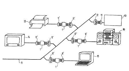
In an arrangement for communicating messages -
which may be telephone calls, faxes, digital data, any
desired audio or video signals, inter alia - via a low-
CA 02337851 2001-O1-16
- 6 -
voltage electricity supply system 9 (Figure 5), which
is preferably situated within a public or private
building or building complex, an apparatus
participating in the exchange of messages, e.g. a PC
10, is directly connected to said mains by its mains
plug 11 being plugged into a mains socket outlet 12
thereof. Via this connection, the PC 10 is on the one
hand supplied with power and, on the other hand, it
exchanges messages with other apparatuses (not
illustrated), which are likewise connected to the low-
voltage electricity supply system 9, via the said
connection and the said low-voltage electricity supply
system. In this case, a carrier frequency which is far
greater than the mains frequency is used, the said
carrier frequency preferably being between 1 MHz and
40 MHz, preferably at least 10 MHz.
Further apparatuses connected to the low-voltage
electricity supply system 9 via mains socket outlets
12' and mains plugs 11' in local proximity to the mains
socket outlet 12, to which the PC 10 is connected, the
said apparatuses not participating in the message
exchange, such as a printer 13, a television set 14, a
terminal 15 and a stereo system 16, may generate
interference signals with high-frequency components,
e.g. during switching processes. If the said
interference signals reach the PC 10, to which the said
apparatuses are connected via short lines associated
with the low-voltage electricity supply system 9,
essentially with no attenuation, they could be
suppressed there only with very complicated measures in
terms of circuitry, or even not at all, and appreciably
interfere with the reception of messages, on which they
are superposed.
For this reason, the apparatuses which are
considered as sources of interference signals are
connected to the low-voltage electricity supply system
9 via an adapter 1 in each case. It is preferable here
for the plug 3 of the adapter 1 in each case to be
plugged directly into the corresponding mains socket
CA 02337851 2001-O1-16
outlet 12', while its socket outlet 4 receives the
mains plug 11' of the apparatus. If extension cables or
distributors are used, the adapter can also be arranged
at a different location. In every case, high-frequency
signals emerging from the said apparatuses, in
particular those signals which lie in the
aforementioned range between 1 MHz and 40 MHz which is
preferred for the exchange of messages, are practically
completely suppressed by the inductor coils 8a, b of
the adapter 1, with the result that they do not
interfere with the reception of messages at the PC 10.
The adapter 1 additionally has the effect of
practically decoupling the cable between the plug and
the respective apparatus for signals of relatively high
frequency, which cable constitutes an open line
termination above all in the case of an unfavourable
length and can cause appreciable interference even when
the apparatus is switched off. As a result, reflections
are suppressed and the sum of the interference signals
on the low-voltage electricity supply system 9 is
reduced further, very substantially so under certain
circumstances.
The reduction of interference enables the data
transmission rates to be considerably increased.
Moreover, the intensity of the carrier signal can be
reduced, thereby making it substantially easier to
comply with legal limitations for the total level of
high-frequency signals on the low-voltage electricity
supply system 9.
Various modifications of the adapter are possible
within the scope of the invention. Thus, by way of
example, it may be designed as a distributor with a
plurality of socket outlets, the mutually corresponding
sockets of the phase conductor and of the neutral
conductor preferably being connected to a single
inductor coil connected downstream of the corresponding
pin. It may also be designed as an extension cable, the
plug, on the one hand, and the socket outlet or else a
plurality of socket outlets, on the other hand, being
CA 02337851 2001-O1-16
_ g _
arranged in two housing parts which are connected by a
three-core cable. The inductor coils are then
accommodated in one of the two housing parts or
distributed between the two. The one-part embodiment
portrayed is preferred, however, owing to its
particularly compact structure and to the fact that it
is simple and clear to use - particularly if the
adapter is plugged directly into the mains socket
outlet in each case.
Of course, the invention can also be used
analogously in low-voltage electricity supply systems
conforming to other standards, e.g. with three phase
conductors.