Note: Descriptions are shown in the official language in which they were submitted.
CA 02337921 2001-02-23
TITLE OF THE INVENTION
PWM CONTROLLED POWER CONVERSION DEVICE
BACKGROUND OF THE INVENTION
1. Field of the Invention
The present invention relates to a power conversion
device that converts AC power and DC power, and more
particularly relates to a PWM controlled power conversion
device wherein the harmonic components contained in the AC
t0 input current waveform are decreased and the efficiency of
power conversion is improved.
2. Description of the Related Art
A power conversion device that converts AC power to DC
power is the PWM controlled AC/DC power conversion device
described in Laid-open Japanese Patent Publication No. H.
10-66343.
The essentials thereof are shown in Figure 1, numeral 1
being an AC power source, numeral 3 being a self-excited
voltage converter, numeral 4-1 and 4-2 being smoothing
capacitors, numeral 5 being the load, and numeral 10 being a
PWM controller. Self-excited voltage converter 3 is an NPC
(neutral point clamped) circuit.
Typically in a PWM controlled AC/DC power conversion
device, sine-wave PWM control is performed based on
triangular wave comparison; however, by setting the
modulation frequency (triangular wave carrier frequency) of
CA 02337921 2001-02-23
PWM control higher than the AC power source frequency, the
harmonic components contained in the input current waveform
on the AC power source side can be reduced.
Figure 2 shows an example of the waveform of such
operation, and shows the sine-wave signal SIN, triangular
wave carrier signals TR1, TR2, the switching signals Gul,
Gu2, Gxl, Gx2 that are applied to the U-phase switching
devices Sul, Su2, Sxl, Sx2 of the self-excited voltage
converter, and the AC-side U-phase voltage waveform Vsu of
l0 the converter. The voltage of the smoothing capacitor is
here taken to be Vd.
In a power conversion device (AC/DC power conversion
device) in which AC power is converted to DC power, if a
large amount of harmonic components are contained in the
IS input current waveform on the AC power source side, this is
a factor causing distortion of the AC system voltage and may
have an adverse effect on other electrical equipment
connected to the same AC system. An AC/DC power conversion
device in which there are few power source harmonics is
20 therefore sought.
PWM control is performed in the AC/DC power conversion
device shown in Figure 1, but in general in AC/DC power
conversion equipment of the PWM controlled type, the
modulation frequency of PWM control must be raised in order
25 to reduce the amount of harmonic components contained in the
AC input current waveform.
2
CA 02337921 2001-02-23
It is therefore an unavoidable requirement to raise the
switching frequency of the switching devices; however, there
is an upper limit to the switching frequency, depending on
the characteristic of the elements of the switching element.
In particular, sufficient harmonic reduction effect was
sometimes not obtained at the upper limiting frequency of
the GTO thyristor elements that are commonly used in high-
capacity power conversion devices. Furthermore, raising the
switching frequency tended to increase switching losses
to generated in the switching element and was associated with a
drop in the power conversion efficiency of the power
conversion device.
Accordingly, an object of the invention of the present
application is to provide a power conversion device capable
of achieving both improved power conversion efficiency and a
reduction in the amount of harmonics of the power source, by
realizing a system in which the harmonic components
contained in the AC input current waveform can be reduced
without raising the switching frequency of the AC/DC power
conversion device.
SUMMARY OF THE INVENTION
Accordingly, one object of the present invention is to
provide a novel power conversion device comprising:
2S an active current control means (unit) that calculates
a phase angle reference value for determining the ON/OFF
3
CA 02337921 2001-02-23
phase based on the AC power source voltage phase from the
deviation with respect to the active current reference value
of the active current that is input to the power conversion
device; and a fixed pulse pattern generating means (unit)
that controls the self-excited voltage power conversion
device by generating a switching signal of fixed pulse
pattern whose fundamental frequency is synchronized with the
AC power source frequency, based on the phase angle
reference value calculated by this active current control
means(unit).
According to the invention of the present application,
even if, for the fixed pulse pattern, a pulse pattern of the
switching signal supplied to the self-excited voltage type
power conversion device is selected such as to produce a
desired value of the harmonic components, it becomes
possible to control the active current supplied to the power
conversion device from the AC power source to a desired
value, thereby making it possible to reduce the harmonic
components contained in the AC input current waveform
without raising the switching frequency of the switching
devices.
Further, in order to achieve the above object,
according to the invention of the present application, there
are provided:
n transformers whose primaries are connected in series
with the AC voltage source and that shift the phase of the
4
CA 02337921 2001-02-23
secondary voltage by 60°/n in each case; and self-excited
voltage converters whose AC sides are connected to the
respective secondary sides of these transformers; and a
pulse pattern generator that produces pulse patterns wherein
the phase of the switching signal that is applied to these
respective self-excited voltage converters is shifted in
each case by 60°/n but is otherwise the same.
With the present application, the amount of harmonic
components contained in the AC input current waveform can
l0 therefore be reduced, thanks to the series multi-connection
effect at the AC input terminal of the self-excited voltage
converters without raising the switching frequency of the
switching devices.
BRIEF DESCRIPTION OF THE DRAWINGS
A more complete appreciation of the present invention
and many of the attendant advantages thereof will be readily
obtained as the same becomes better understood by reference
to the following detailed description when considered in
connection with the accompanying drawings, wherein:
Figure 1 is a layout diagram illustrating a prior art
power conversion device;
Figure 2 is a waveform diagram given in explanation of
the principles of operation of the prior art power
conversion device illustrated in Figure 1;
5
CA 02337921 2001-02-23
Figure 3 is a layout diagram illustrating a first
embodiment of the present invention;
Figure 4 is a waveform diagram given in explanation of
the principles of operation of the first embodiment of the
present invention illustrated in Figure 3;
Figure 5 is a layout diagram illustrating a second
embodiment of the present invention;
Figure 6 is a layout diagram illustrating a third
embodiment of the present invention;
Figure 7 is a layout diagram illustrating a fourth
embodiment of the present invention;
Figure 8 is a layout diagram illustrating a fifth
embodiment of the present invention;
Figure 9 is a layout diagram illustrating a sixth
embodiment of the present invention;
Figure 10 is a layout diagram illustrating a seventh
embodiment of the present invention;
Figure 11 is a voltage-current vector diagram given in
explanation of the principles of operation of the seventh
embodiment of the present invention illustrated in Figure
10;
Figure 12 is a layout diagram illustrating an eighth
embodiment of the present invention;
Figure 13 is a layout diagram illustrating a ninth
embodiment of the present invention;
6
CA 02337921 2001-02-23
Figure 14 is a layout diagram illustrating a tenth
embodiment of the present invention;
Figure 15 is a layout diagram illustrating an eleventh
embodiment of a power conversion device according to the
invention of the present application;
Figure 16 is a waveform diagram illustrating an example
of a fixed pulse pattern in the apparatus of Figure 15;
Figure 17 is a voltage-current vector diagram given in
explanation of the principles of operation of an active
l0 current controller in the apparatus of Figure 15; and
Figure 18 is a voltage-current vector diagram given in
explanation of the principles of operation of a reactive
current controller in the apparatus of Figure 15.
DETAILED DESCRIPTION OF THE PREFERRED EMBODIMENTS
Referring now to the drawings, wherein like reference
numerals designate identical or corresponding parts
throughout the several views, and more particularly to
Figure 3 thereof, one embodiment of the present invention
will be described.
Identical structural elements are given the same
reference symbols and further description thereof is omitted.
(First embodiment)
Figure 3 is a layout diagram of a power conversion
device according to this embodiment. In this case, as an
example, the multi-connection number is taken as n=2.
7
CA 02337921 2001-02-23
In Figure 3, numeral 1 is an AC power source, numeral
2-1 and 2-2 are transformers, numeral 3-1 and 3-2 are self-
excited voltage converters, numeral 4-1 and 4-2 are
smoothing capacitors, numeral S is the load, and numeral 11
is a pulse pattern generator.
Transformers 2-1 and 2-2 have their primary sides
connected in series with the AC power source 1; the phase of
the secondary voltage of 2-1 is advanced by 30° with respect
to that of 2-2. The AC terminals of the self-excited voltage
converters 3-1 and 3-2 are respectively connected to the
secondary side of transformers 2-1 and 2-2.
Smoothing capacitors 4-1 and 4-2 are respectively
connected to the DC side terminals of self-excited voltage
converters 3-1 and 3-2 and are mutually connected in series,
the two ends thereof being connected to DC buses P and N.
Load 5 is connected between the DC buses P and N and may be
for example a voltage inverter.
Pulse pattern generator 11 generates the pattern of the
switching signals that are supplied to the self-excited
voltage converters. The pulse patterns that are supplied to
self-excited voltage converters 3-1 and 3-2 are of identical
pattern, but the phase of the pulse pattern supplied to
self-excited voltage converter 3-1 is advanced by 30° from
that supplied to self-excited voltage converter 3-2.
Figure 4 shows an example of the switching signals Gul,
Gvl, Gu2, and Gv2 supplied to switching devices Sul, Svl,
8
CA 02337921 2001-02-23
Su2, Sv2 of the U-phase and V-phase of the self-excited
voltage converters, the voltage waveforms Vuvl, and Vuv2
between the secondary wirings of the transformers and the
voltage waveform Vsuv across the primary wiring of the
transformers at the AC power source connection point.
The voltage of the smoothing capacitor is here taken to
be Vd.
From Figure 4, it can be seen that, even if the
switching frequency is made the same as the AC power source
frequency, the voltage waveform Vsuv across the AC wiring of
the power conversion device is sine-wave shaped. The
harmonic components contained in the AC input current
waveform are determined by the harmonic components contained
in the converter AC voltage Vsuv, so if the converter AC
voltage Vsuv is sine-wave shaped, the AC input current
waveform is also sine-wave shaped, and the harmonic content
can be reduced.
Consequently, with this embodiment, the harmonic
components contained in the AC input current waveform can be
reduced without raising the switching frequency.
(Second embodiment)
A second embodiment of the present invention is
described below with reference to the drawings. As shown in
Figure 5, this embodiment differs from the first embodiment
in that the self-excited voltage converters 3-3 and 3-4 are
NPC (neutral point clamped) circuits.
9
CA 02337921 2001-02-23
So long as the mufti-connected converters are self-
excited voltage converters as in this embodiment, there is
no particular restriction as to their type.
(Third embodiment)
A third embodiment of the present invention is
described below with reference to the drawings. In this
embodiment, as an example, the mufti-connection number is
taken as n=2.
As shown in Figure 6, this embodiment differs from the
l0 first embodiment in that the smoothing capacitors 4 are
common for the self-excited voltage converters.
With this embodiment, just as in the first embodiment,
the harmonic components contained in the AC input current
waveform can be reduced without raising the switching
frequency.
(Fourth embodiment)
A fourth embodiment of the present invention is
described below with reference to the drawings.
As shown in Figure 7, in this embodiment, the multi-
connection number is taken as n=2 and a three-level voltage
inverter (NPC inverter) is connected as the load. This can
also be applied to be inverters of more levels by increasing
the mufti-connection number.
(Fifth embodiment)
A fifth embodiment of the present invention is
described below with reference to the drawings.
l0
CA 02337921 2001-02-23
As shown in Figure 8, in this embodiment, the capacity
of the power conversion device can be expanded by connecting
a power conversion device of multi-connection number n=2 in
parallel with the AC power source, connecting a smoothing
capacitor in series with the DC side, and supplying DC power
to the load.
(Sixth embodiment)
A sixth embodiment of the present invention is
described below with reference to the drawings.
t0 As shown in Figure 9, this embodiment differs from the
first embodiment in that the pulse pattern generator is a
fixed pulse pattern generator 12.
Consequently, in this embodiment, the fixed pulse
pattern generator 12 generates a fixed pulse pattern
synchronized with the AC power source in accordance with an
arbitrary phase angle reference value a* with respect to the
AC power source voltage. In this case, a specific harmonic
component contained in the AC input current waveform can be
suppressed to a desired value by selecting an pattern such
that the specific harmonic component contained in the fixed
pulse pattern has the desired value.
(Seventh embodiment)
A seventh embodiment of the present invention is
described below with reference to the drawings.
As shown in Figure 10, in this embodiment, active
current controller 13 finds and outputs the phase angle
CA 02337921 2001-02-23
reference value a* of the fixed pulse pattern generated by
fixed pulse pattern generator 12 with respect to the AC
power source voltage by performing proportional integral
control based on the deviation of the active current value
Ip supplied to the power conversion device from the AC power
source and an active current reference value Ip*.
Next, the control action of this embodiment will be
described with reference to Figure 11.
Figure 11 shows a voltage-current vector diagram at a
to given instant, V1 being the primary voltage vector (current
converter AC side voltage) determined by the fundamental
component of the fixed pulse pattern, Is being the AC input
current vector, Vs being the AC power source voltage vector,
and VL being the voltage vector that is applied to the
reactor arranged on the AC side of the power conversion
device or the AC system inductance Ls. The voltage vectors
satisfy the following expression:
VL = Vs - V1 ...(1)
And the AC input current vector Is is given by the
2o following expression:
Is = VL/jc~sLs ...(2)
where cas is the AC power source frequency.
From this condition, considering the case where the
phase angle of the fixed pulse pattern supplied to the power
conversion device with respect to the AC power source
voltage is increased from a to a', the voltage vector that
12
CA 02337921 2001-02-23
is applied to inductance Ls is in accordance with the
following expression:
V'L = Vs - V' 1 ...(3)
And the AC input current vector is in accordance with
the following expression:
I's = V'L/jc~SLs ...(4)
From the above, by increasing the phase angle of the
fixed pulse pattern with respect to the AC power source
voltage, the AC input current is increased, and the active
l0 current component contained therein is also increased.
Contrariwise, by decreasing the phase angle, the active
current component can also be decreased.
with this embodiment, even if the switching signal that
is supplied to the self-excited voltage converter is a fixed
pulse pattern, by changing the phase angle thereof with
respect to the AC power source voltage, the active current
supplied to the power conversion device from the AC power
source can be controlled to a desired value.
(Eighth embodiment)
An eighth embodiment of the present invention is
described below with reference to the drawings.
As shown in Figure 12, in this embodiment, high-pass
filter 14 removes the DC component from the reactive current
value IQ that is supplied to the power conversion device
from the AC power source, thereby detecting the oscillating
component contained in the reactive current; the phase angle
13
CA 02337921 2001-02-23
reference compensation value ~a* is found by multiplying
this by a suitable coefficient and is output.
Adder 15 adds the phase angle reference compensation
value Da* and the phase angle reference value a* and outputs
a corrected phase angle reference value a**. In this
embodiment, if the active current supplied to the power
conversion device from the AC power source is controlled by
changing the phase angle of the fixed pulse pattern,
oscillation of the active current can be suppressed.
(Ninth embodiment)
A ninth embodiment of the present invention is
described below with reference to the drawings.
As shown in Figure 13, in this embodiment, DC voltage
controller 16 performs proportional integral control based
on the deviation of the DC voltage Vd which is the DC side
voltage of the power conversion device and the DC voltage
reference value Vd*, thereby finding an active current
reference value Ip*, which is output.
Consequently, with this embodiment, the DC side voltage
of the power conversion device can be controlled to a
desired value.
(Tenth embodiment)
A tenth embodiment of the present invention is
described below with reference to the drawings.
As shown in Figure 14, in this embodiment, reactive
current controller 17 performs proportional integral control
14
CA 02337921 2001-02-23
based on the deviation between the reactive current value IQ
supplied to the power conversion device from the AC power
source and the reactive current reference value IQ*, thereby
finding a DC voltage reference compensation value ~Vd*,
which is output. Adder 18 adds the DC voltage reference
compensation value OVd* and the DC Voltage reference value
Vd* to obtain a corrected DC voltage reference value Vd**,
which is output.
Consequently, with this embodiment, the reactive
current supplied to the power conversion device from the AC
power source can be controlled to a desired value; in
particular, the AC power source power factor can be
controlled to 1 when the reactive current reference value
IQ* = 0.
(Eleventh embodiment)
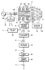
Figure 15 is a block diagram illustrating an eleventh
embodiment of the power conversion device according to the
invention of the present application. The characteristic
features of the apparatus shown in Figure 15 lie in the
internal construction of the PWM controller 10 of Figure 1,
which comprises a reactive current controller 50, limiter 60,
DC voltage controller 70, active current controller 80,
high-pass filter 90, adder 100, and fixed pulse pattern
generator 110.
In Figure 15, an NPC (neutral point clamped) power
conversion device 3 is illustrated as an example of a self-
CA 02337921 2001-02-23
excited voltage power conversion device, but any self-
excited voltage power conversion device could be employed,
there being no particular restriction as to type. Load 5 is
connected to the DC side terminal of the self-excited
voltage power conversion device 3, and may be for example a
voltage inverter.
In the power conversion device of Figure 15, a current
detector 130 and AC detector 140 are provided on the AC side
and a DC voltage detector 150 is provided on the DC side as
l0 means for detecting feedback values for control purposes.
Current detector 130 detects the AC current supplied from AC
power source 1 to power conversion device 3; AC detector 140
calculates the active current Ip and reactive current Iq
supplied from AC power source 1 to power conversion device 3
is using the AC current detected by current detector 130 and
the input voltage of power conversion device 3, and
generates synchronization signal Sy synchronized with the AC
voltage. Active current Ip is supplied as a feedback current
value to the input stage of active current controller 80 and
20 likewise reactive current Iq is supplied to the input stage
of reactive current controller 50 and high-pass filter 90.
The DC side voltage Vd is detected by DC voltage detector
150 and this is supplied as a feedback DC voltage value to
the input stage of DC voltage controller 70.
25 Reactive current controller 50 inputs the deviation of
the reactive current Iq supplied from the AC power source 1
16
CA 02337921 2001-02-23
to the power conversion device with respect to the reactive
current reference value Iq*, and performs control
calculation such as proportional integral control, and
outputs a DC voltage reference value Vd* such as to make
this deviation zero. This DC voltage reference value Vd** is
restricted so that it does not exceed a prescribed amplitude
range by passing it through a limiter 60 and is output as a
new DC voltage reference value Vd**. By comparing the DC
side voltage Vd of the power conversion device with the DC
l0 voltage reference value Vd**, DC voltage controller 70
generates an active current reference value Ip* such as to
make the deviation of these two zero. Active current
controller 80 performs control calculations such as
proportional integral control using the deviation of the
active current Ip supplied from the AC power source 1 to the
power conversion device with respect to the active current
reference value Ip*, and thereby finds and outputs a phase
angle reference value a* corresponding to the ON/OFF phase
of the switching devices of power conversion device 3.
High-pass filter 90 removes the DC component from the
reactive current Iq supplied from the AC power source to the
power conversion device and thereby detects the oscillation
component contained in this reactive current and, by
multiplying this by a suitable coefficient, finds phase
angle reference compensation value ~a*; adder 100 adds this
to the phase angle reference value a* from the active
17
CA 02337921 2001-02-23
current controller 80 to find the compensated phase angle
reference value a**. Fixed pulse pattern generator 110
generates a fixed pulse pattern for controlling power
conversion device 3 in accordance with the phase angle
S reference value a** that is finally obtained. Power
conversion device 3 is controlled by fixed pulse pattern
generator 110 generating a fixed pulse pattern of ON/OFF
phase whose fundamental frequency is synchronized with the
AC power source frequency as switching signal supplied to
l0 power conversion device 3, in accordance with the phase
angle reference value a** with respect to the AC power
source voltage phase.
As an example of the fixed pulse pattern generated by
fixed pulse pattern in generator 110, Figure 16 shows the
15 switching signals GUl, GU2, GX1, GX2 supplied to the U-phase
switching devices SU1, SU2, SX1, SX2 in self-excited voltage
power conversion device 3, and the AC side U-phase voltage
waveform Vsu of self-excited voltage power conversion device
3. It is to be assumed that when a switching signal is "1",
20 the corresponding switching element is in the ON condition
and when it is "0" it is in the OFF condition. The voltages
of the smoothing capacitors 2p and 2n are respectively taken
as Vd. Consequently, the voltage between the DC terminals P
and N is 2Vd.
25 In Figure 16, the number of pulses per AC power source
half-cycle of the fixed pulse pattern is 3 and the ON/OFF
18
CA 02337921 2001-02-23
fundamental phase angle of the fixed pulse pattern is
defined by the phase angles x (ON), y (OFF), z (ON) of first
four half-cycles. These phase angles are:
0° < x < y < z < 90° ...(5)
Taking into account the symmetry of the waveform, the
OFF/ON/OFF phase angles of the second four half-cycles are
determined as:
180 - z, 180 - y, 180 - x ",(6)
likewise the OFF/ON/OFF phase angles of the third four
to half-cycles are determined as:
180 + x, 180 + y, 180 + z ",(
and the OFF/ON/OFF phase angles of the fourth four
half-cycles are determined as:
360 - z, 360 - y, 360 - x ,
..(8)
The harmonic components contained in the AC side U-
phase voltage Vsu of the power conversion device 3 can be
calculated by Fourier expansion of the AC side U-phase
voltage Vsu of Figure 16. By Fourier expansion, the n-th
order harmonic component Vn contained in the AC side U-phase
voltage Vsu of power conversion device 3 is calculated as
follows.
Vn = 4 Vd {cos(nx) - cos (ny) + cos (nz)}/(nn)
... ( 9 )
where n = l, 3, 5, 7, 9, 11...
If no harmonic constituents are present in the AC power
source voltage, the harmonic constituents contained in the
19
CA 02337921 2001-02-23
AC input current of the power conversion device 3 are
determined by the harmonic constituents contained in the
converter AC side voltage. Consequently, by suitably
selecting the phase angles x, y, z so as to reduce the
harmonic components contained in the converter AC side
voltage, the amount of harmonic constituents contained in
the AC input current can be reduced without increasing the
switching frequency.
It should be noted that, although in Figure 16 as an
t0 example of the fixed pulse pattern the case of three pulses
per AC power source half cycle was illustrated, the number
of pulses can be selected at will.
The control action of the active current controller 80
is illustrated with reference to Figure 17. Figure 18 shows
a voltage-current vector diagram at a given instant, Va
being the power conversion device AC side voltage level
determined by the DC side voltage Vd of the power conversion
device and the fundamental component of the fixed pulse
pattern, Is being the AC input current vector, Vs being the
AC power source voltage vector, VL being the voltage vector
applied to a reactor arranged on the AC side of the power
conversion device or to the AC system inductance Ls. Each
voltage vector satisfies the following expression (the
vector symbol is omitted, here and hereinbelow).
VL = Vs - Va ... ( 10 )
CA 02337921 2001-02-23
Also, the AC input current vector Is is given by the
following expression:
I s = VLF (jc~s ~ Ls) ...(11)
where cps is the AC power source frequency.
Considering the case where, from this condition, the
phase angle in the lagging direction with respect to the AC
power source voltage of the fixed pulse pattern applied to
the power conversion device is increased from a to a',
expression (10) changes to the following expression by
change of the voltage level that is applied to inductance Ls
to V'L and the voltage level Va to V'a.
V'L = Vs - V'a ...(12)
Also, the expression for the AC input current vector
becomes the following:
I's = V'L/ (Jws ~ Ls) ...(13)
Consequently, by increasing the phase angle of the
fixed pulse pattern in the lagging direction with respect to
the AC power source voltage, the AC input current Is is
increased and the active current Ip component contained
therein is also increased. Contrariwise, by decreasing the
phase angle in the lagging direction, the active current Ip
component can also be decreased. Furthermore, by controlling
the phase angle in the leading direction, regeneration of
the DC power on the AC side can also be achieved.
With this embodiment, even when the switching signal
that is applied to self-excited voltage power conversion
21
CA 02337921 2001-02-23
device 3 is a fixed pulse pattern, the active current Ip
that is supplied from AC power source 1 to the power
conversion device can be controlled to a desired value by
altering the phase angle with respect to this AC power
source voltage.
As already described, high-pass filter 90 removes the
DC component from the reactive current Iq supplied from AC
power source 1 to the power conversion device and thereby
detects the oscillation component contained in the reactive
l0 current Iq and, by multiplying this by a suitable
coefficient, finds a phase angle reference compensation
value ~a*, which it outputs. This phase angle reference
compensation value ~a* is added to the phase angle reference
value a* to obtain a corrected phase angle reference value
a**. Fixed pulse pattern generator 110 generates a fixed
pulse pattern in accordance with the corrected phase angle
reference value a**.
Thus, thanks to the provision of high-pass filter 90,
oscillation of the active current Ip can be controlled if
the active current Ip that is supplied from the AC power
source 1 to the power conversion device is controlled by
changing the phase angle of a fixed pulse pattern.
However, if there is no need to suppress oscillation of
the active current supplied from the AC power source to the
power conversion device, high-pass filter 90 and adder 100
can be dispensed with.
22
CA 02337921 2001-02-23
DC voltage controller 70 calculates the active current
reference value Ip* using the deviation of the DC side
voltage Vd of the power conversion device and the DC voltage
reference value Vd**, and transmits this to active current
controller 80. Active current controller 80 increases or
reduces the DC side voltage Vd of the power conversion
device by controlling the active current Ip that is supplied
from the AC power source to the power conversion device in
accordance with the active current reference value Ip*.
Thus, by providing a DC voltage controller 70, the DC
side voltage Vd of the power conversion device can be
controlled to a desired value.
If there is no need to control the DC side voltage Vd
of the power conversion device to a desired value, DC
voltage controller 70 can be dispensed with.
Reactive current controller 50 finds the DC voltage
reference value Vd* using the deviation of the reactive
current Iq supplied from the AC power source 1 to the power
conversion device and the reactive current reference value
Iq*, and transmits this to DC voltage controller 70. DC
voltage controller 70 increases or decreases the absolute
value of the power conversion device AC side voltage vector
Va determined by the DC side voltage Vd and the fundamental
component of the fixed pulse pattern by controlling the DC
side voltage Vd of the power conversion device in accordance
with the DC voltage reference value Vd*.
23
CA 02337921 2001-02-23
Figure 18 is a voltage-current vector diagram at a
given instant similar to Figure 17 and describes as an
example the principle of controlling the reactive current Iq
to zero by increasing the AC side voltage vector V'a of the
power conversion device to V~~a in other words the principle
of making Iq = 0 by making the AC input current vector I's
an AC input current vector I~~s of the same phase as AC
power source voltage Vs.
Thus, by providing a reactive current controller 5, the
l0 reactive current Iq that is supplied from the AC power
source 1 to the power conversion device can be controlled to
a desired value: in particular, if the reactive current
reference value Iq* - 0, it is possible to control the AC
power source power factor to 1.
If it is not necessary to control the reactive current
Iq supplied from the AC power source to the power conversion
device to a desired value, reactive current controller 50
can be dispensed with.
Limiter 60 transmits to DC voltage controller 70 a new
DC voltage reference value Vd** obtained by restricting the
DC voltage reference value Vd** that is output by reactive
current controller 100 such that it does not exceed an
arbitrarily specified range. DC voltage controller 70
controls the DC side voltage Vd of the power conversion
device in accordance with DC voltage reference value Vd**.
24
CA 02337921 2001-02-23
With this embodiment, the DC side voltage Vd (or 2Vd)
of the power conversion device can be controlled to within a
desired range.
If there is no need to control the DC side voltage of
the power conversion device to within a desired range,
limn er 60 may be dispensed with.
Although in the embodiments described above, the
individual functional components were described as
consisting of a plurality of discrete components, these
l0 components could be implemented by software using one or
more microprocessors.
With a power conversion device according to the
invention of the present application, the amount of harmonic
components contained in the AC input current can be reduced
without increasing the switching frequency, making it
possible to achieve both an improvement in power conversion
efficiency and reduction in power source harmonics.
Furthermore, according to the invention of the present
application, DC voltage divided in multiple steps could be
2o applied as the DC power source of a multi-level voltage
inverter that converts this into AC voltage.
Furthermore, according to the invention of the present
application, the capacity of a power conversion device could
be expanded by connecting a plurality of power conversion
devices in parallel with an AC power source, and supplying
DC power to a common load.
CA 02337921 2001-02-23
Furthermore, according to the invention of the present
application, by making the pulse pattern of the switching
signal that is supplied to each of the self-excited voltage
type converters a fixed pulse pattern, it becomes possible
to select a pulse pattern such as to reduce the amount of
harmonic components and so to improve the harmonic reduction
effect.
Furthermore, according to the invention of the present
application, the active current that is supplied to the
l0 power conversion device from the AC power source can be
prevented from becoming oscillatory, and can be controlled
in stable fashion.
Furthermore, according to the invention of the present
application, the DC side voltage of the power conversion
device can be controlled to a desired value.
Furthermore, according to the invention of the present
application, the reactive current that is supplied from the
AC power source to the power conversion device can be
controlled to a desired value.
2o Furthermore, according to the invention of the present
application, the active current that is supplied from the AC
power source to the power conversion device can be prevented
from becoming oscillatory, thereby enabling stable control
to be achieved.
26
CA 02337921 2001-02-23
Furthermore, according to the invention of the present
application, the DC side voltage of the power conversion
device can be controlled to a desired value.
Furthermore, according to the invention of the present
application, the reactive current that is supplied from the
AC power source to the power conversion device can be
controlled to a desired value.
Furthermore, according to the invention of the present
application, the DC side voltage of the power conversion
device can be restricted to within a desired range.
Thus, although the present invention has been shown and
described with respect to exemplary embodiments thereof, it
should be understood by those skilled in the art that the
foregoing and various other changes, omissions and additions
may be made therein and thereto, without departing from the
spirit and scope of the present invention.
27