Note: Descriptions are shown in the official language in which they were submitted.
CA 02338058 2001-O1-17
WO 00/04407 PCT/US99/15956
SMALL INLET OPTICAL PANEL AND A METHOD OF MAKING
A SMALL INLET OPTICAL PANEL
CROSS REFERENCE TO RELATED APPLICATIONS
This application is a continuation-in-part of U.S Patent Application Serial
Number
09/118,270, filed 7/17/98, and entitled "SMALL INLET OPTICAL PANEL".
STATEMENT REGARDING FEDERALLY SPONSORED RESEARCH OR DEVELOPMENT
o This invention was made with Government support under contract number
DE-AC02-98CH10886, awarded by the U.S. Department of Energy. The Government
has
certain rights in the invention.
BACKGROUND OF TIDE INVENTION
Field of the Invention
The present invention is directed generally to a planar optical display, and,
more
particularly, to a small inlet optical panel and a method of making a small
inlet optical panel.
Description of the Background
2o It is known in the art to form an optical panel from a plurality of stacked
waveguides.
The waveguides collectively define an inlet face at one end of the waveguides
and an outlet face
at an opposite end. The outlet face may be disposed obliquely with the inlet
face. The outlet
CA 02338058 2001-O1-17
WO 00/04407 PCT/US99/15956
face may form an small acute face angle with the longitudinal axes of the
waveguides, thus
allowing the height of the screen to be substantially larger than the depth or
thickness of the
panel. The panel inlet face generally extends the full width of the panel
correspondent to the
width of the outlet face, but is very narrow due to the thinness of the panel.
For example, where
an inlet face has a width of 133 cm, the corresponding length in the prior art
would be 2.54 cm.
The narrow inlet face necessitates the use of a complex light projection
system for
distributing and focusing the image light across the full width and depth of
the panel, thereby
allowing for accurate display on the outlet face. This complex light
projection system increases
the complexity and cost of the overall system, and increases the space
requirements of the
display panel.
Therefore, the need exists for a waveguide optical panel having an aperture
inlet which
allows for simplification of light projection and focusing at the inlet,
without a loss of image
resolution at the outlet face.
~5 BRIEF SUMMARY OF THE INVENTION
The present invention is directed to a small inlet optical panel, which
includes a first
plurality of stacked optical waveguides which forms an outlet face body with
an outlet face,
which includes a second plurality of stacked optical waveguides which forms an
inlet face body
with an inlet face, and an optical coupling element connected to the first
plurality and to the
2o second plurality, wherein the optical coupling element redirects light
along a parallel axis of the
inlet face to a parallel axis of the outlet face. In the preferred embodiment
of the present
invention, the inlet face is disposed obliquely with and askew from the outlet
face.
CA 02338058 2001-O1-17
WO 00/04407 PCT/US99/15956
The present invention is also directed to a method of making a small inlet
optical panel
which includes individually coating a plurality of glass sheets in a substance
having an index of
refraction lower than that of the glass sheets, stacking the plurality of
coated glass sheets,
wherein each coated glass sheet is fastened to an adjoining glass sheet using
an adhesive,
applying pressure to the stack. curing the adhesive, cutting the stack to form
an outlet face body
having a first wedge shape with an outlet face thereon, repeating the
individually coating. the
stacking, the applying, and the curing to form a second stack, cutting the
second stack to form an
inlet face body having a second wedge shape correspondent to the first wedge
shape and having
an inlet face thereon. and joining together the inlet face body and the outlet
face body at an
1o optical coupling element, wherein the outlet face is disposed askew from
the inlet face, for
redirecting light incident into the inlet face body to a direction incident
into the outlet face body.
The present invention solves difficulties encountered in the prior art by
providing a
waveguide optical panel having a small aperture inlet, which allows for
simplification of light
projection and focusing at the inlet, without a loss of image resolution at
the outlet face.
I5
BRIEF DESCRIPTION OF THE SEVERAL VIEWS OF THE DRAWINGS
For the present invention to be clearly understood and readily practiced, the
present
invention will be described in conjunction with the following figures,
wherein:
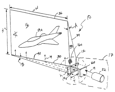
FIG. 1 is an isometric view schematic illustrating a small inlet optical
panel;
2o FIG. 2 is an isometric view schematic illustrating a horizontal and
vertical cross-section of
a small inlet optical panel;
CA 02338058 2001-O1-17
WO 00/04407 PCT/US99/15956
FIG. 3 is a schematic illustrating an exagerrated horizontal and vertical
cross section of the
small inlet optical panel;
FIG. 4 is a horizontal and vertical cross section of the small inlet optical
panel illustrating
an alternative embodiment of the panel using one plurality of waveguides;
FIG. ~ is an isometric view schematic illustrating an alternative embodiment
of the small
inlet optical panel which includes an optical coupler in the form of a
holographic optical element;
FIG. 6 is an isometric view schematic illustrating an alternative embodiment
of the small
inlet optical panel wherein the inlet face is coplanar with the outlet face;
and
FIG. 7 is an isometric view schematic illustrating an alternative embodiment
of the small
to inlet optical panel wherein the inlet face is opposite the outlet face.
DETAILED DESCRIPTION OF THE INVENTION
It is to be understood that the figures and descriptions of the present
invention have been
simplified to illustrate elements that are relevant for a clear understanding
of the present
15 invention, while eliminating, for purposes of clarity, many other elements
found in a typical
optical display panel. Those of ordinary skill in the art will recognize that
other elements are
desirable and/or required in order to implement the present invention.
However, because such
elements are well known in the art, and because they do not facilitate a
better understanding of the
present invention, a discussion of such elements is not provided herein.
20 FIG. 1 is an isometric view schematic illustrating a small inlet optical
panel 10. The
display panel 10 includes an inlet face 12 for receiving light 14. and an
outlet face 16 disposed
obliquely with and askew from the inlet face 12 for displaying light 14. The
light 14 is generated
4
CA 02338058 2001-O1-17
WO 00/04407 PCT/US99/15956
by a light generator 17. The inlet face 12 and outlet face 16 are each formed
by a plurality of
waveguides 12a, 16a, wherein one end of each waveguide 12a, 16a forms an inlet
for that
waveguide 12a, 16a, and wherein the opposite end of each waveguide 12a, 16a
forms an outlet
for that waveguide 12a, 16a.
The inlet face 12 is preferably disposed generally perpedicular to and askew
from the
outlet face 16 for receiving the light 14 from the modulator 20 and projector
22. The horizontal
extension of each waveguide 12a of the inlet face 12 is disposed below and
substantially
perpendicular to the horizontal extension of each waveguide 16a of the outlet
face 16. The
plurality of stacked waveguides 12a of the inlet face 12 extends vertically.
1 o Each waveguide 16a extends horizontally, and the plurality of stacked
waveguides 16a
extends vertically, along the outlet face 16. The light 14 is displayed on the
outlet face 16 in a
form such as, but not limited to, a video image 14a. The outlet face 16 may be
generally formed
into a triangular wedge having an acute face angle A between the bottom 30 of
the body 32 of the
outlet face 16 and the back 34 of the body 32 of the outlet face 16. The acute
face angle A may
be in the range of about 5 to 10 degrees, for example, with the panel 10
increasing in thickness
from a minimum at the top 36 of the body 32 of the outlet face 16, to a
maximum thickness at the
bottom 30 of the body 32 of the outlet face 16. The maximum thickness may be
chosen as small
as is practicable in a given application. The panel 10 has a height from the
top to the bottom of
the outlet face 16, and a width from the left to the right of the outlet face
16. The width and
2o height may be selected to produce width to height aspect ratios of 4:3 or
16:9, for example, for
uses such as a typical television application. In an exemplary embodiment of
the outlet face 16
of the present invention, a maximum thickness in the range of about $ cm may
be chosen, in
5
CA 02338058 2001-O1-17
WO 00/04407 PCT/US99115956
conjuction with a height of 100 cm and a width of 133 cm. The left to right
width of the inlet
face 12 is chosen to be the same as the maximum thickness T of the panel 10.
The inlet face 12
has a suitable vertical height h, which is a matter of design choice. The
inlet face 12 has a width
to height aspect ratio which, for the purpose of ease of interface with the
outlet face 16, is
preferably also 4:3. Correspondingly, the panel 10 diverges in two wedge
shapes, one from the
bottom 30 to the top 36 of the outlet face body 32, and the second at the
bottom 30 of the outlet
face body 32, from the left of the interface 40 to the inlet face 12.
The disposition of the inlet face 12 with the outlet face 16 necessitates the
redirection of
the light 14, which light 14 is incident on the inlet face 12 in an
approximately horizontal plane
~ 0 and must be redirected to a vertically upwardly direction through the
waveguides 16a of the
outlet face 16. This periscopic optical path permits the use of a relatively
small area modulator
20 at the bottom of the panel 10 to provide a small aperture light source
which is expanded
through the panel 10 for display on the outlet face 16 at a substantially
increased viewing area.
The light generator 17 generates light 14 and passes the light 14 to inlet
face 12, and the
surface area of light generation immediately adjacent to the inlet face 12
preferably is equivalent
to the surface area of the inlet face 12. The light generator 17 may include a
light source 22, a
light modulator 20, or imaging optics. The light 14 may be initially generated
by the light source
22. The light source 22 may be, for example, a bright incandescent bulb, a
laser, a plurality of
phosphors, at least one LED, at least one OLED, at least one FED, or a
projector. The light 14
2o from the source 22 is preferably collimated. The light 14 may be modulated
by the modulator 20
for defining individual picture elements, known in the art as pixels. The
modulator 20 may take
a form known in the art, such as, but not limited to, a liquid crystal display
(LCD), a Digital
6
CA 02338058 2001-O1-17
WO 00/04407 PCT/I3S99/15956
Micromirror Device (DMD), a GLV, a raster scanner, avector scanner, a PDLC, an
LCOS, a
MEMS, and a CRT. The imaging optics may include light folding mirrors or
lenses. The
imaging optics may be optically aligned between the inlet face 12 and the
light modulator 20 for
compressing or expanding and focusing the light 14 as required to fit the
inlet face 12. The
modulated light 14 is generally incident on the inlet face 12 from the imaging
optics as a
compressed image which is transmitted horizontally through the inlet face 12,
turned for
transmission vertically upwardly through the outlet face body 32 for display,
and expands for
suitable horizontal and vertical resolution and scale.
FIG. 2 is an isometric view schematic illustrating a horizontal and vertical
cross-section
t0 of a small inlet optical panel 10 of FIG. 1. The panel 10 includes a first,
or top, plurality of
stacked optical waveguides 16a forming an outlet face 16, a second, or bottom,
plurality of
stacked waveguides 12a stacked perpendicularly to the outlet face 16 to form
an inlet face 12
below the bottom 30 of the body 32 of the outlet face 16, and a light
redirection element 50
disposed inside the panel 10 at the interface 40 between the inlet face
waveguides 12a and the
15 outlet face waveguides 16a for redirecting the light 14 for periscopic
transmission through the
waveguides 12a, 16a.
The waveguides 12a, 16a are configured in two independent groups with the
first
plurality of waveguides 16a forming a wedge defining the outlet face 16 and
the interface 40.
The second plurality of waveguides 12a are disposed below the light
redirection element 50 at
2o the interface 40, and forms a wedge defining the inlet face 12. The second
plurality of
waveguides 12a are configured in a wedge correspondent to the wedge shape of
the outlet face
body 32. The body 32 of the outlet face 16 wedge receives the light 14 for
transmission
CA 02338058 2001-O1-17
WO 00/04407 PCT1US99/15956
vertically upwardly to the outlet face 16. The body 32 of the outlet face 16
receives light 14
along the surface of the bottom 30 of the body 32, adjacent the light
redirection element 50. The
light 14 received at the bottom 30 of the body 32 is passed through the body
32, and is displayed
on the outlet face 16. The body 60 of the inlet face 12 wedge receives the
light 12 at its vertical
inlet face 12 for transmission substantially horizontally to emission at the
light redirection
element 50. -The inlet face 12 may be sized to match the area of the modulator
20 for receiving
the light 14, and the inlet face 12 is also substantially smaller in area than
the interface 40 at the
light redirection element S0. The angle A of the outlet face 16 wedge may be
about 5 to 10
degrees, and the second angle B of the inlet face 12 wedge is then be suitably
smaller.
l0 The plurality of stacked waveguides 12a, 16a used to form the inlet face 12
and the outlet
face 16 may be formed of any material known in the art to be suitable for
passing
electromagnetic waves therethrough, such as, but not limited to, glass,
plastics, or polymers. The
preferred embodiment of the present invention is implemented using individual
glass sheets,
which are typically approximately 2 - 40 microns thick. Two different
thicknesses of glass sheet
I5 may be used simultaneously in a given application of the present invention,
one to form the
outlet face 16, and one to form the inlet face 12. In the preferred embodiment
of the present
invention, the glass sheets used within the inlet face 12 are approximately
the same thickness,
and the glass sheets used within the outlet face 16 are approximately the same
thickness. The
glass used may be of a type such as, but not limited to, glass type BK-7, or
may be a suitable
2o plastic laminate, such as Lexan~, commercially available from the General
Electric Company~.
The waveguides 12a, 16a are discussed with more particularity with respect to
FIG. 3.
CA 02338058 2001-O1-17
WO 00/04407 PCT/US99/15956
The light redirection element 50 is disposed between the body 60 of the inlet
face 12 and
the body 32 of the outlet face 16. The light redirection element 50 may be,
for example, an
optical coupling element, and may be fastened to each plurality of waveguides
12a, 16a using
methods known in the art, such as an optically transparent epoxy. The function
of the coupler SO
is to redirect the initially horizontally directed light 14 from the bottom
plurality of waveguides
12a vertically upwardly into the top plurality of waveguides 16a. Both the
waveguides 12a, 16a
and the coupler 50 of the present invention are passive optical devices. The
light redirection
element 50 is discussed with more particularity with respect to FIG. 3.
FIG. 3 is a schematic illustrating an exagerrated horizontal and vertical
cross section of
1o the small inlet optical panel 10 embodied in FIG. 2. The light redirection
element 50 redirects
the light 14 flowing into the inlet face 12, which then flows through the
bottom plurality of
waveguides 12a and is thereby incident on the light redirection element 50, to
flow into the top
plurality of waveguides 16a, and thereby be incident on the outlet face 16.
The light redirection
element 50 preferably includes a plurality of fresnel prismatic grooves SOa
which are straight
15 along the width of the bottom waveguides 12a in the direction of the panel
thickness T for
redirecting the image light 14 vertically upwardly into the top plurality of
waveguides 16a. In a
preferred embodiment, the light redirection element 50 is an optical coupler
50 in the form of a
Transmissive Right Angle Film (TRAF) II, which is commercially available from
the 3M
Company of St. Paul, Minnesota. The TRAF II coupler 50 is effective for
turning the image
20 light at an angle of up to approximately 90°. In an alternative
embodiment of the present
invention, the light .redirection element 50 may be in the form of a
diffractive grating 50, which
diffractive grating 50 includes an extremely small series of straight gratings
configured for
9
CA 02338058 2001-O1-17
WO 00/04407 PCT/US99/15956
optically diffracting the light 14 in order to turn the light flowing
substantially horizontally
through the bottom plurality of waveguides 12a vertically upwardly into the
top plurality of
waveguides 16a. The diffractive grating 50 has a lower turning angle
capability than the TR.AF
II embodiment.
An individual waveguide 12a, 16a used in the present invention typically
includes a
cental core 100 laminated between cladding layers 102, a receiving end 104,
and an outlet end
106. The central core 100 channels the image light 14 through the waveguide
12a, 16a, is
disposed between cladding layers 102, and extends from the receiving end 104
to the outlet end
106. The central core 100 is, in the preferred embodiment, a glass sheet of
thickness T in the
1 o range between 2 and 40 microns, as discussed hereinabove. The central core
100 has a first
index of refraction. The cladding layers 102 also extend from the receiving
end 104 to the outlet
end 106. The cladding layers 102 may be black in color to improve contrast and
brightness.
Alternatively, a black layer may be disposed between adjoining cladding layers
102 for
absorbing ambient light at the outlet end 106, where the adjoining cladding
layers 102 are
transparent. The term black is used herein to encompass not only pure black
color, but
additionally, any functionally comparable dark color suitable for use in the
present invention,
such as dark blue. The cladding layers 102 have a second index of refraction,
lower than that of
the central core 100, for ensuring total internal reflection of the image
light 14 as it travels from
the receiving end 104 to the outlet end 106.
2o The top plurality 16a and the bottom plurality 12a of stacked waveguides
may be made
by several methods. A plurality of glass sheets may be individually coated
with, or dipped
within, a substance having an index of refraction lower than that of the
glass, and a plurality of
CA 02338058 2001-O1-17
WO 00/04407 PCT/LTS99/15956
coated sheets may then be fastened together using glue or thermally curing
epoxy. Alternatively,
the glue or epoxy could form the cladding layers and be applied directly to
the glass sheets. In
one embodiment of the present invention, a first coated or uncoated glass
sheet is placed in a
trough sized slightly larger than the first coated glass sheet, the trough is
filled with a thermally
curing black epoxy, and the coated or uncoated glass sheets are repeatedly
stacked at an angle,
forming a layer of epoxy between each coated or uncoated glass sheet. The
stacking is
preferably repeated until between approximately 500 and 800 sheets have been
stacked. The
number of waveguides 16a which are stacked to form the outlet face 16 are
selected for
providing a corresponding vertical resolution of the outlet face 16. For
example, 525 of the
o waveguides 16a may be stacked in the outlet face 16 to produce 525 lines of
vertical resolution in
the outlet face 16. Uniform pressure may then be applied to the stack,
followed by a cure of the
epoxy, and a sawing of the stack into a wedge shape of an angle dependant on
the use of the
stack as an outlet face 16 or an inlet face 12. The wedge may be sawed curved
or flat, and may
be frosted or polished after sawing.
FIG. 4 is a horizontal and vertical cross section of the small inlet optical
panel 10
illustrating an alternative embodiment of the panel 10. In this alternative
embodiment, the top
plurality of waveguides 16a extend vertically, continuously from the outlet
face 16 to the side
inlet face 12, with the interface 40 being horizontal and disposed at the
bottom edge 30 of the
outlet face 16.
2o In this alternative embodiment, the light redirection element SOc, is
disposed at the
bottom of the panel 10 and is inclined from the inlet face 12 at the right
side of the outlet face 16
to the opposite side of the outlet face 16. The bottom of the plurality of
waveguides 16a, as well
tt
CA 02338058 2001-O1-17
WO 00/04407 PCT/US99/15956
as the element SOc, are therefore inclined at the small acute angle B from the
bottom of the panel
10, thereby defining a bottom wedge portion. Also in this alternative
embodiment, the element
SOc includes a plurality of tilted reflective facets or mirrors 50c optically
aligned between the
inlet face 12 and the interface 40 for reflecting the substantially
horizontally directed light 14
vertically upwardly to the outlet face 16.
FIG. 5 is an isometric view schematic illustrating an alternative embodiment
of the small
inlet optical panel 10, and includes a light redirection element SOd in the
form of a holographic
optical element SOd configured to reflect the image light 14 from the inlet
face 12 across the
interface 40 for display on the outlet face 16. The holographic coupler 50d
may take a
to conventional form known in the art for turning the light 14 from a
substanitally horizontal
direction to the vertical direction required for internal transmission through
the top plurality of
waveguides 16a to the outlet face 16.
FIG. 6 is an isometric view schematic illustrating an alternative embodiment
of the small
inlet optical panel 10, including a top plurality of waveguides 16a configured
as in the above
embodiments. The alternative embodiment of FIG. 7 also includes a bottom
plurality of
waveguides 12a which are continuous along the full width W of the outlet face
16 and are
stacked vertically. In this embodiment, the inlet face 12 extends the full
width W of the outlet
face 16 directly below the outlet face 16 at the front of the panel 10.
FIG. 7 is an isometric view schematic illustrating an alternative embodiment
of the small
2o inlet Optical panel 10, wherein the inlet face 12 extends the full width W
of the outlet face 16, but
is disposed at the back of the panel 10.
12
CA 02338058 2001-O1-17
WO 00/04407 PCT/US99/15956
Those of ordinary skill in the art will recognize that many modifications and
variations of
the present invention may be implemented. The foregoing description and the
following claims
are intended to cover all such modifications and variations.
Ij