Note: Descriptions are shown in the official language in which they were submitted.
CA 02338106 2001-O1-18
WO 00/05792 PCT/US99/15892
-1-
HIGH POWER LATERALLY ANTIGUIDED SEMICONDUCTOR
LIGHT SOURCE WITH REDUCED TRANSVERSE OPTICAL
CONFINEMENT
FIELD OF THE INVENTION
This invention pertains generally to the field of semiconductor diode
lasers and amplifiers and particularly to antiguided diode lasers and
amplifiers.
BACKGROUND OF THE INVENTION
Semiconductor diode lasers are formed of multiple layers of
semiconductor materials. The typical semiconductor laser includes an n-type
layer,
a p-type layer, optical confinement layers and an undoped active structure
between
them such that when the diode is forward biased electrons and holes recombine
in
the active structure with the resulting emission of light. The layers
surrounding the
active structure typically have a lower index of refraction than the active
structure
and form a dielectric waveguide that confines the emitted light transversely
to the
active structure. Semiconductor lasers may be constructed to be either edge
emitting or surface emitting.
To confine the emitted light laterally, positive-index guided or
negative-index guided (antiguided) structures may be employed in a laser or
amplifier diode array. In a positive-index guided structure the refractive
index is
highest in regions where the laser light has high field intensity and is low
in regions
of low field intensity, effectively trapping light within the high-index
regions, i.e.,
the laser array elements. in a negative-index guided or antiguided structure,
the
refractive index is lowest and the optical gain is highest in regions where
the laser
light has maximum field intensity, i.e., the laser array elements, and the
refractive
index is highest and there is little or no optical gain in regions that
contain relatively
CA 02338106 2001-O1-18
WO 00/05792 PCT/tJS99/15892
-2-
low field intensity. Consequently, some of the generated light will pass into
the
higher refractive index interelement regions and thus will not be confined to
the
lasing element regions, but this lost light is compensated for by the excess
gain in
the array element regions.
$ An array of laser emitters can typically oscillate in several possible
modes. In a fundamental or in-phase array mode, all emitters oscillate in
phase with
each other, and a far field pattern is produced in which most of the energy is
concentrated in a single lobe which is ideally diffraction limited. In
general, there
are many possible array modes for a multiple element array, and many laser
arrays
operate in two or three array modes simultaneously and produce beams that are
typically two or three times wider than the diffraction limit. The problems
associated with the operation of laser arrays at high power with high beam
quality
are discussed in U.S. Pat. No. 4,985,897, entitled Semiconductor Laser Array
Having High Power and High Beam Quality. That patent describes a laser diode
array structure, which may be implemented in an antiguided configuration,
operated
at or near the in-phase-mode resonance condition for which coupling occurs
equally
between all elements of the array.
The development of high-power (greater than one watt) coherent
diode laser sources has been an area of continued research efforts. Positive
index-
guided single-element devices have been demonstrated up to about 0.6 watt (W)
continuous wave (CW) coherent power, with reliable operation demonstrated to
about 0.2 W, primarily being limited by the relatively small waveguide width
of ~3
pin. Single-element antiresonant reflecting optical waveguide (ARROW) lasers
have also demonstrated single-mode optical power up to ~0.5 W, with the added
benefit of a drive-independent beam pattern, due to strong lateral optical-
mode
confinement in devices of 4-6 pin aperture width. See L.J. Mawst, D. Botez, C.
Zmudzinski, and C. Tu, "Design optimization of ARROW-type diode lasers," IEEE
Photon. Technol. Lett., Vol. 4, pp. 1204-1206, November 1992. In fact, single-
mode ARROW devices with aperture width of up to 10 pin are possible, which
CA 02338106 2001-O1-18
WO 00/05792 PCT/US99I15892
-3-
should allow for reliable powers of ~0.5 W CW from devices with nonabsorbing
mirrors.
Research on phase-locked diode laser arrays in an attempt to increase
the aperture width and operating power met with little success in controlling
the
complicated mode structure until the development of resonant-optical-waveguide
(ROW) antiguided arrays. Such arrays are described in D. Botez, L.J. Mawst,
G.L.
Peterson, and T.J. Roth, "Phase-locked arrays of antiguides: Modal content and
discrimination," IEEE J. Quantum Electron., Vol. 26, pp. 4$2-495, March 1990.
Antiguided arrays have demonstrated near-diffraction-limited CW operation at 1
W
from a 120 p.m aperture, with up to 0.6 W in the central lobe of the far-field
emission pattern, and reliable operation over 3500 hours has been achieved at
0.5 W
CW output, thus making ROW arrays the only high-power coherent device type to
date that has demonstrated long-term reliability. However, since such devices
are
based on meeting a (lateral) optical resonance condition, the fabrication
tolerances
on their structural parameters have been experimentally and theoretically
determined
to be very tight, especially as the number of elements increases. See D.
Botez, A.
Napartovich, and C. Zmudzinski, "Phase-locked arrays of antiguides: Analytical
theory II," IEEE J. Quantum Electron., Vol. 31, pp. 244-253, February 1995.
A semiconductor laser having antiguide elements and interelement
structures with high loss coefficient is described in U.S. Patent 5,606,570 to
Botez,
et al. , entitled High Power Antiguided Semiconductor Laser with Interelement
Loss.
Such a structure can be used to provide excellent discrimination between the
resonant in-phase mode and the unwanted nonresonant modes, and allows
relatively
large fabrication tolerances.
Currently, in symmetric transverse waveguide lasers, the power can
be significantly increased by increasing the waveguide for the same quantum-
wells)
size. In turn, the transverse optical confinement factor t (the percent of
light
energy in the active region) decreases significantly, which, in turn, provides
a large
equivalent transverse spot size, d/r, where d is the quantum-wells) total
thickness.
The lowering of r does not significantly affect the threshold-current density
as long
CA 02338106 2001-O1-18
WO 00/05792 PCT/US99/15892
-4-
as the internal loss coefficient is small (1-2crri'), and the cavity length is
increased
roughly in the same proportion that r was decreased. Using such structures,
very
high spatially incoherent powers (e.g., 8-10 W CW) have been achieved from
broad-stripe (100 Vim) devices. However, since transversely the optical mode
hardly penetrates into the cladding layers, it is practically impossible to
obtain
effective lateral mode confinement for 2-D spatial-mode coherence.
SUMMARY OF THE INVENTION
In accordance with the present invention, semiconductor light
emitting sources such as lasers and amplifiers are formed in multilayer
semiconductor structures that incorporate antiguided lateral confinement of
emitted
light. The semiconductor structure of the invention also incorporates an
asymmetric
transverse optical waveguiding structure to provide a large equivalent
transverse
spot size. In addition, the effects of intra element gain spatial hole burning
are
significantly reduced, allowing the core elements to be made significantly
larger
than conventional cores. These features enable semiconductor light sources
having
a significantly increased overall spot size as compared to similar
semiconductor
structures formed in a conventional manner. Spot sizes up to five times larger
than
conventional structures are quite feasible, enabling five times more reliable
power
for semiconductor lasers incorporating such structures or five times higher
saturated
power P~~ for semiconductor amplifiers.
The semiconductor light emitting source of the invention is comprised
of a multilayer semiconductor structure including, in the transverse
direction, a
substrate, an active region, and confinement and cladding layers on each side
of the
active region to surround the active region. At least one core element or
element
region is formed laterally in the structure at which light emission primarily
occurs
and interelement regions are formed adjacent to the core element. The core
element
has a selected effective refractive index for the emitted light and the
effective
refractive index of the interelement regions is higher than that of the core
element to
provide effective antiguiding of light generated in the active region. The
optical
confinement and cladding layers on opposite sides of the active region have
different
CA 02338106 2001-O1-18
WO 00/05792 PCT/US99/15892
_>_
indexes of refraction to provide an optical waveguiding structure in the
transverse
direction in the core element which is asymmetrical and which favors lasing
only in
the transverse fundamental optical mode. Preferably, the optical confinement
and
cladding layers provide an optical confinement factor in the active region of
less
than about 2 % , and wherein there is an effective refractive index step
between the
core element and the interelement regions lower than about 0.05 and an
attenuation
coefficient in the interelement regions lower than about 100 cm'. Where the
semiconductor source is to be operated as a laser, means for providing optical
feedback are incorporated in the structure to provide lasing action in the
core
elements. For incorporation in an amplifier, facets at the longitudinal edges
of the
semiconductor structure are formed to be sufficiently antireflective so that
the
semiconductor source operates as an amplifier.
The present invention can be configured using various lateral
antiguided structures, including as a simplified ARROW structure, as a single
core
element ARROW structure, or as a multicore (e.g., three) ARROW structure.
Plural core elements may be separated by interelement regions to define a ROW
array. If desired, the ARROW structure may be tapered longitudinally so that
the
core element is wider at one edge of the structure than at the other edge.
Various
means may be provided in the semiconductor structure to restrict current
applied to
the structure to the core element.
Further objects, features and advantages will be apparent from the
following detailed description when taken in conjunction with the accompanying
drawings.
BRIEF DESCRIPTION OF THE DRAWINGS
In the drawings:
Fig. 1 is a simplified diagram illustrating the profile of the index of
refraction and the optical mode profile in the transverse direction in the
light
emitting core element of the semiconductor source of the invention.
Fig. 2 is a simplified diagram illustrating the index of refraction
profile and the optical mode profile in the transverse direction in the
interelement
CA 02338106 2001-O1-18
WO 00/05792 PCT/US99/15892
-6-
regions that are adjacent to the core element (or elements) in the
semiconductor
source of the invention.
Fig. 3 is a diagram of an exemplary transverse index profile in the
core element of a semiconductor source laser of the invention having an
InGaAsP
active region with InGaAs double quantum wells.
Fig. 4 is a diagram of an exemplary transverse index profile in the
higher effective refractive index interelement regions that are adjacent to
the core
element having the profile shown in Fig. 3.
Fig. 5 is a diagram of another exemplary transverse index profile in
the higher effective refractive index interelement regions that are adjacent
to the
core element having the profile shown in Fig. 3.
Fig. 6 is an illustrative cross-sectional view through a semiconductor
source in accordance with the invention having a simplified ARROW (S-ARROW)
lateral configuration.
Fig. 7 is a partial cross-sectional view of a portion of an exemplary
current blocking structure for the source of Fig. 6.
Fig. 8 are graphs illustrating calculated edge radiation losses as a
function of passive waveguide thickness in the clad regions for the
fundamental
mode and the first order mode for the source of Fig. 6.
Fig. 9 is an illustrative cross-sectional view through a semiconductor
source in accordance with the invention having a single core and an ARROW
lateral
structure.
Fig. 10 is a plan view of the core element and adjacent elements for
an ARROW structure as in Fig. 9 which has tapered lateral dimensions.
Fig. 11 are graphs illustrating calculated edge reflection losses versus
passive waveguide thickness in the clad regions for the semiconductor source
of Fig.
9, illustrating the fundamental mode (mode 4) and higher order modes.
Fig. 12 is an illustrative cross-sectional view of a semiconductor
source in accordance with the invention having a triple core ARROW lateral
structure.
CA 02338106 2001-O1-18
WO 00/05792 PCT/US99l15892
_7_
Fig. 13 are graphs illustrating calculated edge reflection losses as a
function of passive waveguide thickness for the semiconductor source of Fig.
12
with a core width of 8.5 pin for the fundamental mode (mode 8), adjacent
modes,
and out-of-phase modes.
Fig. 14 are calculated graphs for the laser of Fig. 12 as in Fig. 13
calculated for a core width of 10 pin.
Fig. 15 is a simplified diagram of transverse index of refraction
profile and optical mode profile of a core element having a narrow light trap
separated from a narrow active region.
Fig. 16 is a simplified diagram of transverse index of refraction
profile and optical mode profile for the interelement structures adjacent to
the core
element of Fig. 15.
Fig. 17 is an exemplary cross-sectional view through a semiconductor
source structure in an AIGaAs based system comprising a single-clad ARROW
structure.
Fig. 18 is an exemplary transverse index of refraction profile in the
core element for the source structure of Fig. 17.
Fig. 19 is a table showing exemplary layer thicknesses and Al
percentages for each of the layers in the semiconductor structure of Fig. 18
(top
row) as well as for those for an interelement region (bottom row).
DETAILED DESCRIPTION OF THE INVENTION
The present invention allows the attainment of higher power levels in
semiconductor lasers and amplifiers (generally referred to herein as
semiconductor
sources) by achieving lateral mode confinement for two-dimensional spatial-
mode
coherence. Large transverse spot size (d/r) as well as strong lateral mode
confinement are obtained utilizing an asymmetric transverse optical
waveguiding
structure. A simplified diagram illustrating an exemplary asymmetric
transverse
index of refraction profile in the core element of the source structure of the
invention is illustrated in Fig. 1. The index of refraction is at a first
level 20 in a
lower cladding layer, at a second higher level 21 in a confinement layer, at a
higher
CA 02338106 2001-O1-18
WO 00/05792 PCT/US99/15892
_g_
index level 22 in the active region (which is of width d), at a level 23
{which is the
same as the level 21) in the top confinement layer adjacent to the active
region, and
at a lower level 24 in an upper cladding layer that is at a higher level than
the lower
cladding index level 20. The thickness of the upper confinement layer 23 is
also
preferably greater than that of the lower confinement layer 21. The result is
an
optical mode profile illustrated by the graph 26. Such a structure allows
lasing only
in a single (optical) transverse mode which has a d/r value at least three
times
higher than that of conventional symmetric-guide laterally antiguided coherent
laser
structures.' The core element, the profile of which is illustrated in Fig. 1,
is
bounded laterally by interelement regions which, for an antiguided structure
in
accordance with the invention, have a higher effective refractive index than
that of
the core element. As illustrated in Fig. 2, the index profile in the
interelement
region may have the same layers of index levels 20, 21, 22, 23 and 24 as the
core
element and an additional layer of high refractive index level 28 which
provides a
higher effective refractive index for the entire interelement or boundary
region than
that of the core element. The optical mode profile in the interelement region
is
illustrated by the graph 29 in Fig. 2. As illustrated in Figs. 1 and 2, there
is
sufficient field overlap between the fields in the core element and the
interelement
regions to provide adequate lateral antiguiding.
A semiconductor source structure with a core element having an
asymmetric index profile, as illustrated in Fig. 1, bounded by higher
effective index
interelement regions, as illustrated in Fig. 2, has two main advantages due to
its
relatively small r value, the first being a large equivalent transverse spot
size, d/r,
and the second being that the effects of intraelement gain spatial hole
burning are
significantly reduced, allowing the core elements to be larger than in
conventional
laser structures by a factor proportional to 1/~r . For example, if T is
reduced
three times from 4.3 % (typical for conventional laser structures) to 1.3 % ,
then d/1,
triples and the core element size can be increased by a factor of ~3 . Thus,
the
overall spot size increases by a factor of about 5. A five times larger spot
size
implies that five times more reliable power can be obtained for lasers and a
five
CA 02338106 2001-O1-18
WO 00/05792 PCT/US99/15892
-9-
times higher saturation power, Psa" can be obtained for amplifiers. As an
example,
for typical 3p.m wide ridge-guide type devices, with nonabsorbing mirrors, the
typical reliable single-mode power level is about 0.2 W. Thus, for an aperture
five
times larger, reliable operation in a single spatial mode can be obtained at
five times
S this power, e.g., 1 W continuous wave (CW).
A first exemplary embodiment of the invention is illustrated in Fig.
3, which is an aluminum free active region structure ideally suited for the
etch and
regrowth techniques that are needed to make large lateral spot size antiguided
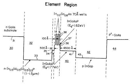
structures. The exemplary structure of Fig. 3 includes a substrate 30 of n-
type
GaAs having a refractive index level 31, a lower cladding layer 32 of n-type
Ino.S(Alo.SGao,S)o.sP having a lower index of refraction level 33 (with a
width of e.g.,
0.7 to 1.5 Vim), a lower confinement layer 34 of InGaAsP having an index level
35
and a width of, e.g. 500 A, an active region 36 having an index level 37 for
InGaAsP barrier layers and a double well quantum structure, each well formed
of
Ino,2Gao,8As (with exemplary dimensions of 70 A for each of the wells and 100
A
spacing between the wells 38 and between the wells and the edges of the active
region), an upper confinement layer 40 having an index level 41 (e.g., 6500 A
wide), and an upper cladding layer 42 having an index level 43. It is
understood, of
course, that reference to "upper" and "lower" are for convenience only, and
simply
distinguish between layers on one side or the other of the active regions. As
illustrated, the index level 43 of the upper cladding layer 42 is higher than
the index
level 33 of the lower cladding layer 32. The upper cladding layer 42 is formed
of p-
type InGaP. The index profile of an exemplary interelement region is
illustrated in
Fig. 4. The structure of the interelement region is similar to that of the
core
element except for the addition of a layer 50 of n-type GaAs within the upper
cladding layer 42 having a higher level 51 of index of refraction than the
index level
43 of the cladding layer 42. An alternative interelement region index profile
is
shown in Fig. 5. It is similar to that shown in Fig. 4 except that the layer
50 of n-
type GaAs includes a thin layer 52 of Ino.zGao.BAs (e.g., 70 A wide) within
the layer
50. The layer 50 provides a greater effective index of refraction for the
CA 02338106 2001-O1-18
WO 00/05792 PCT/US99/15892
-10-
interelement region than the effective index of the core element. Layer 52 in
Fig. 5
introduces interelement absorption loss for devices that need it for
intermodal
discrimination (e.g., triple-core ARROW laser structures). A p+ type GaAs
contact layer 44 may be formed on top of the cladding layer 42.
The structure of Fig. 3 is designed to favor lasing only in the
fundamental transverse optical mode. To assure asymmetry, the lower cladding
layer 32 is n-type InGaAIP, a material of higher band gap and lower index of
refraction than the upper cladding layer 42 (of p-type InGaP).
The transverse structures illustrated in Figs. 3, 4 and 5 may be
utilized in various lateral geometries in accordance with the invention. A
first such
lateral structure is a simplified ARROW (S-ARROW) configuration illustrated at
53
in Fig. 6. The S-ARROW configuration is an ARROW structure with only one
antiresonant interelement region on each side of the single core element. As
used
herein, the interelement regions may be located at the lateral boundaries of a
single
core element, or may be between multiple core elements and at the boundaries
of the
outermost elements. The S-ARROW structure has the advantage of being much
simpler to fabricate than conventional single core ARROW or multiple core
ARROW devices, and it has only two competing lateral modes so that it is
relatively
easy to obtain effective intermodal discrimination. The core element 54 may be
formed having the layer structure illustrated in Fig. 3, utilizing a separate-
confmement-heterostructure (SCH) double-quantum-well (DQW) active region. It
is
bounded by interelement regions 55 whose layer structure is shown in Fig. 4,
which
in this case serve as boundary regions since there is a single core element,
and the
interelement regions include the higher index region 50 as well as additional
layers
of n-type AIInP 57 and n-type GaAs 58 which extend across the entire
structure.
The n-type regions 57 and 58 provide a back biased n-p junction with the p-
type
layer 42. Thus, when voltage is applied between conductive electrodes 60 and
61
formed on the opposite faces of the semiconductor structure 53 to supply
current
across the structure, the current is restricted by the back biased p-n
junctions to the
core element 54 so that light emission occurs in the quantum well layers 38,
CA 02338106 2001-O1-18
WO 00/05792 PCT/US99/15892
-11-
embedded in the active region 36, primarily or entirely in the core element.
Various other alternative means for restricting the current flow to the core
element
may be utilized. These include incorporating an oxide layer at the top of the
p+-
GaAs layer 44 that has a stripe-shaped opening above the core element 54, the
stripe
opening having a width that is narrower than the width of the core (e.g., ? pm
stripe
width for d~o,e=10 ~.m) and centered above the core. Thus, when current is
applied
to the electrode 60 the current flows only through the oxide-defined stripe
contact.
Another alternative is illustrated in Fig. 7 in which a layer of n-type GaAs
is formed
at the top of the layer 42 of p-type InGaP to form a back biased p-n junction.
An
oxide layer 64 may be formed over the entire structure except at an opening 65
at
which a conductive impurity material (e.g., Zn) may be diffused through the
opening 65 and through the p-n junction between the layers 63 and 42 to define
a
conductive contact region 66, as illustrated in Fig. 7, that extends through
the p-n
junction and lies above the core element 54. Another means to restrict current
flow
to the core element is to exploit the technique of selective wet oxidation of
AIGaAs.
This is discussed in, e.g., K.D. Choquette, K.M. Geib, C.I.H. Ashby, R.D.T.
Westen, O. Blum, H.Q. Hou, D.M. Follstaedt, B.E. Hammons, D. Mathes, R.
Hull, "Advances in Selective Wet Oxidation of AIGaAs Alloys," IEEE J. Selected
Topics in Quantum Electronics, Vol. 3, No. 3., June 1997, pp. 916-925.
Selectively oxidized thin layers of Al-containing compound can be formed on at
least one side of the active region to define a stripe opening or openings
adjacent the
core element region. For example, a layer of high Al content (x ? 0.95)
AlxGa,_xAs
can be embedded within the upper or lower cladding layers (layers 42 or 22 in
Fig.
6), or used to replace layer 57 in Fig. 6. Post-growth processing involves
selective
wet oxidation of the AIXGa,_xAs layer outside the core element, initiated from
the
lateral edges of the device structure.
The boundary interelement regions 55 function as lateral cladding
regions for the simplified ARROW structure 53 and are selected to correspond
approximately to the antiresonance condition for the fundamental lateral mode.
The
high index interelement cladding regions 55 support both even and odd
transverse
CA 02338106 2001-O1-18
WO 00/05792 PCT/US99I15892
-12-
modes, which cause lateral antiguidance and guidance, respectively. The theory
and
construction of such simplified core ARROW structures is discussed further in
I . V .
Goltser, L.J. Mawst, and D. Botez, "Single-Cladding Anti-Resonant Reflecting
Optical Waveguide-Type Diode Laser," Optics Letters, Vol. 20, No. 21, November
1, 1995 , pp . 2219-2221.
An example of this structure was modeled, utilizing the MODEM
code for two-dimensional (2D) calculations described in D. Botez, "High-Power
Monolithic Phase-Locked Arrays of Antiguided Semiconductor Diode Lasers,"
Proc. IEE - J, Vol. 139, No. 1, February 1992, pp. 14-23. The following key
parameters are used: r =1.45 %a , d~ =10 pm, interelement region width s =
2.55 pm,
and index step 0n=0.022. Calculated graphs showing edge radiation losses are
shown in Fig. 8 for the fundamental mode at 68 and for the first order mode at
69.
Such calculations show a discrimination of 10 to 15 cm' over a wide range in
the
GaAs passive waveguide thickness. For the exemplary structure of the
invention,
d~=10~m and d~,;~e/r is approximately equal to 1.0 pm. In comparison, for a
conventional simplified ARROW (S-ARROW) with d~=4-6 p.m, and T'=4.3%,
da~,~~e~r is about equal to 0.3 p,m. Thus, for the exemplary structure of the
invention, the lasing spot is 1.7 times larger laterally and three times
larger
transversely than the conventional S-ARROW, i.e., the lasing spot is five
times
greater in area than that for a conventional S-ARROW structure.
It is understood that mirrored facets may be provided at the
longitudinal end edges of the structure to provide optical feedback for lasing
action
in a conventional manner. Alternately, feedback may be provided by a buried
DFB
grating in case single-frequency operation is needed as well.
A conventional ARROW structure with a single core element 54 is
illustrated in Fig. 9. In this conventional structure, an additional layer 71
of n-type
GaAs is formed over the layers 57 and 58 and is spaced from the layer 50 by an
opening 72. The structure of Fig. 9 may be longitudinally uniform or, as
illustrated
in Fig. 10, tapered such that the width d~ of the core element 54 at the front
edge 74
CA 02338106 2001-O1-18
WO 00/05792 PCT/US99/15892
-13-
of the laser structure is greater than at the back edge 75. The edges 74 and
75 may
be mirrored facets for optical feedback.
Conventional ARROW devices have been found to work well
(including single mode high power devices) as long as the core element width
dale,
is less than or equal to about 4 pm. Above this width for the core element,
significant problems are encountered, since a high order mode can be excited
at high
drive levels. 2D calculations done in MODEM for a single core ARROW device in
accordance with the present invention with r=1.45%, ~n=0.022, and with various
core widths d~ore up to 10 pm, show that significant improvements over
conventional
ARROW structures can be obtained. The results of calculations for d~ore=10
p.m, an
emission wavelength ~,=0.98 Vim, and a width s of the reflecting interelement
regions 59 equal to 2.5 pm, are shown in Fig. 11, which illustrates for the
fundamental mode (mode 4) and first order and higher modes edge radiation
losses
versus the GaAs passive guide layer (layer 50) thickness in the lateral clad
regions
59. For d~=10 pm, the fundamental mode has very small losses (less than 1
cni'),
which is much less than for the S-ARROW . Intermodal discrimination is high,
in
the range of 10 to 15 cm' over a wide range in passive-guide layer thickness.
Although mode 7 may be a problem above threshold, a tapered ARROW structure
may be utilized, as shown in Fig. 10, because mode 7 is too lossy to be a
problem if
d~ is less than about 6 p.m, and thus a tapered ARROW design with d~,ba~k = 4
pm
and d~,fTO"~ = 10 pm will suppress mode 7. Again, a lasing spat size having an
area
at least five times greater than that of a conventional ARROW device is
obtained.
The present invention may also be incorporated into mufti-core (e.g.,
three core) ARROW devices. An example of a three-core ARROW structure in
accordance with the invention is illustrated in Fig. 12. All interelement
regions
have the transverse structure shown in Fig. 5. The three core elements 54 are
separated by interelement regions 59" which have the same multilayer structure
as
the boundary interelement regions 59' . The ARROW edge structures defined by
the
layers 71, 57 and 58 and the gap 72 are similar to the ARROW structure of Fig.
9
with the exception that layer 71 includes the absorbing layer 52 shown in Fig.
5.
CA 02338106 2001-O1-18
WO 00/05792 PCT/US99/15892
-14-
For a triple-core ARROW device, the aperture is three times larger than for an
S-
ARROW or a conventional single-core ARROW device, but only about 60% of the
light resides in the far-field central lobe. Thus, about twice the single mode
power
is obtained compared to S-ARROW and ARROW devices, with 2 W CW
diffraction-limited power being obtainable. Graphs illustrating calculated
mode
losses versus passive guide thicknesses for the triple-core ARROW are shown in
Fig. 13 for a core element width equal to 8.5 pm. and in Fig. 14 for a core
element
width of 10 Vim. For both sets of calculations, the width of the boundary
interelement regions 59' is 2.55 pm and the width of the interelement regions
59" is
1.7 Vim, which corresponds approximately to resonant optical transmission
between
the three core elements. For a core element 54 width equal to 10 pm, it is
seen that
the in-phase mode {the fundamental mode) has low loss, about 0.5 cni', and
that the
intermodal discrimination is large (greater than 4 cm') over a wide range in
guide-
layer thickness variation (due to about 66 cm' interelement absorption loss).
It is
seen that the spot size for such devices is again about five times that of the
conventional triple-core ARROW device. The structure of multi-core and
particularly three-core ARROW devices with interelement loss is described in
the
aforesaid U.S. Patent No. 5,606,570 to Botez, et al., entitled "High Power
Antiguided Semiconductor Laser With Interelement Loss."
The present invention may also be incorporated in ROW arrays.
Typically, a 20 element, 120 ~m aperture antiguided array (a so-called ROW
array)
will provide 0.5 to 0.6 W coherent reliable power. Tripling or quadrupling the
value of d/r, the reliable power scales accordingly to 1.5 to 2 W. By
utilizing
nonabsorbing mirrors, it is possible to increase the reliable coherent power
to 3-5
W.
For conventional flared-antiguided MOPA's 130 p,m wide aperture
devices have been demonstrated as shown in D. Botez, M. Jansen, C. Zmudzinski,
L.J. Mawst, P. Hayashida, C. Tu and R. Nabiev, "Flat-Phase Front Fanout-Type
Power Amplifier Employing Resonant-Optical-Waveguide Structures, Appl. Phys.
Lett., Vol. 63, No. 23, Dec. 1993, pp. 3113-3115. By tripling or quadrupling
the
CA 02338106 2001-O1-18
WO 00/05792
-15-
PCT/U 599/15892
transverse spot size in accordance with the present invention, and using
nonabsorbing mirrors, the reliable power obtainable with such devices may be
increased to 3 to 5 W of reliable spatially and temporally coherent power.
The invention may also be applied to ARROW amplifiers, which
comprise ARROW or S-ARROW devices. The devices with r = 1.45 % and 0n =
0.022 may be utilized with up to 10 ~m wide core element size d~. The same
structure is utilized for amplifiers as was described above for lasers except
that the
end facets are anti-reflective (AR) coated (preferably less than 0.1 %
reflectivity) to
prevent lasing oscillation. Another alternative for amplifiers is to utilize
angle-
striped devices (2-7° with respect to the cleaved facets) with low
reflective (LR)
coating (about 1 % reflectivity). Because the spot size of a single-mode
device
increases five-fold, the implications are that for unsaturated regime
amplifier
devices (e.g., for fiber optic communications), the saturated power (P~,) will
increase five times to 50 mW compared to a conventional value of 10 mW . Such
power levels will enable transparent switching networks utilizing such
devices. For
saturated-regime devices, 2 to 4 mm long devices will provide 0.8-1.0 W
amplified
power. By utilizing proper facet passivation, such power may be delivered
reliably,
enabling high powered tunable single-frequency sources (for example, where the
amplifier is placed at the output of an external-cavity-controlled diode
laser).
As a further alternative, the low index core element may be formed
asymmetrically in the transverse direction but of two waveguides rather than
one: a
narrow guide incorporating the active region and a wide guide to spread out
the
mode and make it asymmetric with respect to the active region, as illustrated
in Fig.
15. The core element region may include an index profile as illustrated in
Fig. 15
having a base index level 80, a light trap at a higher index level 81
separated from
an active region and confinement layers 82 by a lower index level region 83,
and an
upwardly adjacent layer at again a lower index level 84. The resulting optical
mode
profile is illustrated by the graph 86. The light trap has a width such that
d~0(n2) is
less than ~,/4. The interelement region shown in Fig. 16 has an additional
light trap
layer 87 that is separated from the active region/confinement layers 82, with
a field
CA 02338106 2001-O1-18
WO 00/05792 PCT/US99/15892
-16-
distribution as illustrated by the graph 88 in Fig. 16. The field
distributions provide
enough overlap for effective lateral antiguiding.
The present invention may also be incorporated in aluminum based
devices, e.g., AIGaAs based. A schematic structure for an S-ARROW device in
such a material system is illustrated in Fig. 17. This device includes an
AIGaAs n-
type cladding layer 90, a confinement layer 91, a double quantum well active
region
92, and an upper confinement layer 93. The structure of Fig. 17 has a further
AIGaAs layer 94 within which is formed a stop-etch layer 96 of GaAs.
Additional
layers of GaAs 97 and GaAs 98 are formed over it, with wells 99 formed at
spaced
positions, as described further below. The structure further includes a p-type
cladding layer 100 of AIGaAs and a p+ capping layer of GaAs 101. Current
confinement may be obtained by utilizing V-grooves (e.g., 2-3 pin wide)
outside the
high-index regions, together with oxide-defined stripes, a preferential Zn
diffusion
(as illustrated in Fig. 7), proton implantations, or oxide-defined stripes
narrower
than the core region. Conducting electrodes 103 and 104 may be formed on the
top
and bottom of the structure to apply power thereto, as desired, with the
former
made taking into account the current confinement scheme. The core element 105
is
defined between the wells 99, which themselves define the interelement regions
106.
An exemplary confinement layer, active region and cladding layer structure
diagram
in Fig. 18, illustrates the index profile for such a structure in the core
element
region, and Fig. 19 illustrates the exemplary constituents and thicknesses of
the
layers for both the core element region 105 (Fig. 17), as well as for the
interelement
region 106. The following key parameters are used: I'= 1.38%, d~=lOpm,
interelement region width s~2.5pm, and index step On~0.023 (in the 2-D MODEM
calculation).
It is understood that the invention is not confined to the particular
embodiments set forth herein as illustrative, but embraces all such forms
thereof that
come within the scope of the following claims.