Note: Descriptions are shown in the official language in which they were submitted.
CA 02338114 2001-O1-18
WO 00/76068 PCT/US00/15533
SINGLE RAIL DOMINO LOGIC FOR FOTJR-PHASE CLOCKING SCHEME
BACKGROUND OF THE INVENTION
The present invention relates generally to digital electronic circuits. and
more particularly
relates to domino logic circuits.
Modern integrated circuits are required to perform ever increasing tasks, and
at ever
increasing operating speeds. The requirement to increase operating speeds has
often been met
by increasing the clock speed at which a circuit operates. For example. while
integrated circuit
operation once occurred at clock speeds on the order of 10 to 50MHz, clock
speeds now are often
significantly greater than 1 OOMHz, and in some cases are even on the order of
400MHz or more.
Increasing clock speeds, however, is not the only method available to circuit
designers to
increase the speed at which circuit operations occur. Circuit designers have
also implemented
circuitry which operates in a staged manner. with each stage evaluating over
only a portion of a
clock cycle and subsequent stages evaluating over subsequent portions of the
clock cycle. That
is, circuit designers arrange logic operations in a sequential manner, with
each logic cell in the
sequence providing information to subsequent logic cells in the sequence.
These logic cells are
evaluated during only a portion of the clock cycle, with subsequent logic
cells evaluated in
subsequent portions of the clock cycle. These logic cells therefore operate in
a domino manner,
and are often referred to as domino logic cells. The use of domino logic
circuits allows designers
to increase the effective speed of logic components without resorting to
increasing clock speed.
In order to allow logic cells to evaluate their inputs in less than an entire
clock cycle logic
cells are often precharged. Precharging the logic cell is accomplished by
driving the logic cell
either to a mid range or to a high state. Driving the logic cell to a mid-
range state allows the logic
cell to change state with only a slight change in voltage. Thus the logic cell
is able to change
state at a faster rate than otherwise would occur. More often, however, the
outputs of logic cells
are driven to a high state. This is because PMOS transistors generally have a
relatively large rise
time due to parasitic capacitances. Accordingly, logic cell operation response
time may be
increased by charging the output to a high level prior to evaluation of the
logic cell.
In a single clock cycle, therefore, a logic cell must be precharged, and
thereafter allowed
to evaluate its inputs. This is often accomplished by precharging the logic
cell during one-half
of a clock cycle, and allowing the logic cell to evaluate its inputs during
the other half of the
clock cycle. One constraint of such a methodology. however, is that the logic
cell must evaluate
and provide its outputs to a subsequent logic cell in one half of the clock
cycle. Further.
subsequent precharging of the logic cell during the first half of a subsequent
clock cycle may
modify the outputs of the logic cell. Accordingly, the logic cell should not
begin precharging
until after the subsequent logic cell has evaluated its inputs.
In order for domino logic circuits to meet such requirements, particularly
when the circuits
are also operating at high clock speeds, the derivation and use of additional
signals based on the
CA 02338114 2002-12-17
output of the logic cell should be kept to a minimum. One such additional
signal is a
complement of the output signal. Forming a complement of the output signal,
using
an inverter for example, poses several problems. The additional inverter used
to form
the output signal complement places a delay in a signal path of an input to
the
subsequent logic stage, thereby limiting the period in which the logic cell
has to
evaluate its inputs. Further, this delay effects only the complementary signal
path
(ignoring fan out related delays), and the output signal path does not include
this
delay. Accordingly, changes in the output signal during subsequent precharging
are
not delayed by the inverter in the signal path of the output complement
signal. Thus,
the period in which the subsequent logic cell may evaluate its input, starting
from the
time when the complementary output of the logic cell goes valid and ending at
the
time the effects of precharging propagate to the output signal of the logic
cell, is
reduced due to the use of the output signal complement.
Therefore, when use of an output signal complement is desired a dual rail, as
opposed to signal rail, domino logic design is generally used. Single rail
designs
generally only have a single output per logic cell. Thus, a single rail design
is
monotonic in nature. In a dual rail design a first set of logic cells produces
a set of
signals, and a second set, or rail, of logic cells produces the complements of
these
signals. Dual rail designs, however, require significantly greater number of
gates than
a single rail design, resulting in increased chip layout space as well as
increased
power consumption.
The requirement for increased functionality of integrated circuits, thus,
results
in a need to decrease the area occupied by logic while also increasing the
size of the
integrated circuit as a whole. To the extent the need for increased
functionality
outstrips the ability to decrease gate size and increase chip die size, chip
area is placed
at a premium. The use of dual rail designs, therefore, impacts the ability of
designers
to provide increased functionality in integrated circuits.
SUMMARY OF THE INVENTION
Thus, the present invention provides a domino logic circuit providing both an
output signal and a complement of the output signal. The present invention
includes a
logic circuit with a precharger. A logic circuit with a precharger includes a
logic cell
-2-
CA 02338114 2002-12-17
and a precharged circuit including multiple transistors. In another
embodiment, the
invention comprises a single rail domino logic circuit. The single rail domino
logic
circuit includes a plurality of logic cells providing information. The logic
cells are
arranged in a sequence from a first logic cell to a last logic cell, with each
of the logic
cells subsequent in the sequence providing information from a prior logic
cell. Each
of the logic cells has an associated precharged circuit, and each of the
precharged
circuits comprises a pair of transistors.
In accordance with one aspect of the invention, there is provided a single
rail
domino logic circuit comprising a plurality of logic cells in a sequence, the
logic cells
providing an output and a complement of the output to succeeding logic cells
in the
sequence, a plurality of precharge circuits, a precharge circuit coupled to
each logic
cell, each precharge circuit including a first transistor and a second
transistor, with the
first transistor and the second transistor receiving clock signals out of
phase with each
other.
In accordance with another aspect of the invention, there is provided a single
rail domino logic circuit comprising a plurality of logic cells providing
information,
the logic cells being arranged in a sequence from a first logic cell to a last
logic cell,
each of the logic cells subsequent in the sequence from the first logic cell
being
provided an information signal and a complement information signal from a
prior
logic cell in the sequence, and a plurality of precharge circuits, each of the
precharge
circuits being coupled to a corresponding one of the plurality of logic cells,
and each
one of the precharge circuits comprising a pair of transistors, the pair of
transistors
receiving two clock signals, the two clock signals being out of phase with
each other.
In accordance with another aspect of the invention, there is provided a single
rail domino logic circuit comprising a plurality of logic cells, each of the
logic cells
producing a corresponding output signal, a plurality of driving inverters,
each of the
driving inverters being coupled to a corresponding logic cell so as to receive
the
corresponding output signal and to propagate the inverse of the corresponding
output
signal to a subsequent logic cell, a plurality of complementary inverters,
each of the
complementary inverters being coupled to a corresponding driving inverter so
as to
receive the inverse of the corresponding output signal and to propagate a
complement
of the inverse of the corresponding output signal to a subsequent logic cell,
a plurality
-2a-
CA 02338114 2002-12-17
of first PMOS precharge transistors, each of the plurality of first PMOS
precharge
transistors being coupled to a corresponding one of the plurality of logic
cells by their
sources, and a plurality of second PMOS precharge transistors, each of the
plurality of
second PMOS precharge transistors being coupled to a corresponding one of the
plurality of first PMOS precharge transistors.
In accordance with another aspect of the invention, there is provided a method
of producing data using a single rail domino logic circuit using a four-phase
clock
comprising precharging a first logic cell in a first quarter clock cycle,
evaluating
inputs to the first logic cell to produce a first logic cell output and a
first logic cell
complementary output and precharging a second logic cell in a second quarter
clock
cycle, and holding the first logic cell output and the first logic cell
complementary
output.
Many of the attendant features of this invention will be more readily
appreciated as the same becomes better understood by reference to the
following
detailed description considered
-2b-
CA 02338114 2001-O1-18
WO 00/76068 PCT/US00/15533
in connection with the accompanying drawings in -which like reference symbols
designate like
parts throughout.
DESCRIPTION OF THE DRAWINGS
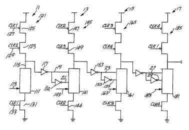
FIG. 1 is a semi-schematic semi-block diagram of a domino logic circuit of the
present
Invention;
FIG. 2 is a timing diagram of clock signals generated by a four-phase clock
used in the
present invention; and
FIG. 3 is a timing diagram of operation of the domino logic circuit of the
present
invention.
DETAILED DESCRIPTION
FIG. 1 illustrates a single rail domino logic circuit of the present
invention. The domino
logic circuit has a first stage 11. a second stage 13, a third stage 15, and a
fourth stage 17. The
first stage provides a first stage output signal 19, and its complement 21, to
the second stage.
Similarly, the second stage provides the third stage a second stage output
signal 23, and its
complement 25, to the third stage, and the third stage provides a third stage
output signal 27, and
its complement 29, to the fourth stage. Thus, the four stages are arranged in
a domino fashion,
with subsequent stages following preceding stages. Further, each stage
provides a differential,
i.e., complementary. output signal to a subsequent stage.
The domino logic circuit is provided four clock signals forming a four phase
clocking
scheme. This is accomplished by having each of the four clock signals be of
the same frequency,
but phase shifted with respect to the other clock signals in ninety degree
increments. The clock
signals, therefore, are symmetrically phase-shifted. Each stage receives two
of these clock
signals.
The first stage includes NMOS first stage logic circuitry I 11 which acts on
logic inputs
113. Coupled to the first stage Logic circuitry is precharge circuitry 121.
The precharge circuitry
is a stacked PMOS pair, with a source of a first PMOS transistor 12~ connected
to a power
supply and a source of a second PMOS transistor 123 connected to the drain on
the first PMOS
transistor. The drain of the second PMOS transistor is, in turn, connected to
the logic circuitry.
A gate of the first PMOS transistor of the precharge circuitry is provided a
first clock
signal (CLK1 ). A gate of the second PMOS transistor is provided a second
clock signal (CLK2).
The first and second clock signals are of the same frequency, but the second
clock signal is phase
shifted by 90° with respect to the first clock signal. Thus, the second
clock signal has a rising
edge delayed by a quarter clock cycle compared to the first clock signal.
Likewise, a falling edge
of the second clock signal is delayed by a quarter clock cycle compared to a
falling edge of the
first clock signal. This is illustrated graphically in FIG. 2. As is
illustrated in FIG. 2, at time t,
the first clock signal has a rising edge. while the second clock signal
remains low. A quarter
-3-
CA 02338114 2001-O1-18
WO 00/76068 PCT/US00/15533
1 clock cycle later, at time t3, the second clock signal leas a rising edge.
Similarly, a quarter clock
cycle after time t;, namely at time t4, the first clock signal has a falling
edge while the second
clock signal remains high. At time t5, which is a quarter clock cycle after
time t4, the second
clock signal has a falling edge.
As the first and second clock signals are provided to the gate of the first
PMOS transistor
and the gate of the second PMOS transistor, respectively, the first and second
PMOS transistors
are both on only when both the first clock signal and the second clock signal
are low. As the first
clock signal and the second clock signal are both low only for a quarter of
each clock period, the
precharge circuitry unly precharges the NMOS logic for a quarter clock cycle.
In addition, the
drain of the second PMOS transistor is connected to an inverter 117. The
inverter 117 provides
the first stage output. One of the primary purposes of the inverter 117 is to
drive the first stage
output signal to the succeeding stage. In addition, the first stage output is
provided to a second
inverter I 19. The second inverter provides the complement of the first stage
output signal and
similarly serves to drive the complement of the first stage output signal to
the succeeding stage.
The logic circuitry I 11 is also connected to a drain of an NMOS driving
transistor 131.
The gate of the driving transistor 131 is provided the first clock signal.
Thus, when the first clock
signal goes high the driving transistor becomes active and the logic circuitry
evaluates its inputs.
As the precharge circuitry becomes inactive when the first clock signal goes
high, the output of
the first stage is dependent on the inputs of the logic circuitry.
Accordingly, for every complete
clock cycle the first stage will precharge during a quarter of the clock
cycle, and hold its output
for three-quarters of the clock cycle at which time precharging once again
occurs.
The second stage is similar to the first stage. The second stage includes
second stage logic
circuitry 141. The second stage logic circuity receives logic inputs 143, as
well as the
complementary outputs from the first stage. The second stage also has
precharge circuitry 145
comprising a stacked PMOS pair of transistors 147 and 149. The stacked PMOS
pair of the
second stage receives as inputs to their gates the second clock signal and a
third clock signal
(CLK3). The third clock signal is delayed by a quarter clock cycle with
respect to the second
clock signal, and is therefore 90° out of phase from the second clock
signal and 180° out of
phase from the first clock signal. Thus, whereas the first stage precharges
between times t, and
t,, the second stage precharges between times t~ and t;. Accordingly, the
second stage operates
with a quarter clock cycle delay as compared to the first stage.
The drain of the second PMOS transistor 149 is connected to an inverter 153.
The
inverter 153 acts as a driving inventor, and produces the second stage output.
The second stage
output is also provided to an inventor 155 which provides the complement of
the second stage
output. The second stage output and the complement of the second stage output
are provided to
the third stage.
The second stage logic circuitry 111 is also connected to a drain of an NMOS
driving
transistor 144. The gate of the driving transistor I 44 is provided the second
clock signal. Thus,
-4-
CA 02338114 2001-O1-18
WO 00/76068 PCT/US00/15533
1 when the first clock signal goes high the driving transistor becomes active
and the logic circuitry
evaluates its inputs. As the precharge circuitry becomes inactive when the
second clock signal
goes high, the output of the first stage is dependent on the inputs of the
logic circuitry.
Accordingly. for every complete clock cycle the first stage will precharge
during a quarter ofthe
S clock cycle and hold its output for three-quarters of the clock cycle at
which time precharging
once again occurs.
The third stage is similar to the first and second stages. As with the first
and second
stages. the third stage includes logic circuitry 161 having as inputs the
second stage output and
the complement of the second stage output, as well as logic inputs 163.
Coupled to the logic
circuitry is precharge circuitry 165. As with the first and second stages, the
precharge circuitry
includes a stacked PMOS pair. The gates of the stacked PMOS pair are provided
the third clock
signal and a fourth clock signal (CLK4). The fourth clock signal is 90
° out of phase from the
third clock signal, and 270 ° out of phase from the first clock signal.
Thus, the third stage logic
circuitry is precharged beginning at time t3 until time t4.
The fourth stage is similar to the first, second, and third stages. As with
the prior stages,
the fourth stage includes logic circuitry 181 having as inputs the third stage
output and the
complement of the third stage output, as well as logic inputs 183. Coupled to
the logic circuitry
is precharge circuitry 185. As with the prior stages, the precharge circuitry
includes a stacked
PMOS pair. The gates of the stacked PMOS pair are provided a fourth clock
signal and the first
clock signal. Thus, the fourth stage logic circuitry is precharged beginning
at a time t4 until time
t5, and evaluates beginning at time t5.
FIG. 3 illustrates the timing diagram of the operation of the domino logic
circuit of FIG.
1 when supplied the clock signals of FIG. 2. At time t, the second clock
signal goes low, and the
first clock signal is already low. Slightly after time t,, therefore, a signal
S"S at the drain of the
second PMOS transistor 123 goes high. Using .25 micron technology, the change
in the signal
S"5 occurs approximately .2 nanoseconds after the second clock signal goes
low. Thus, shortly
after the second clock signal goes low at time t, the first domino logic stage
begins precharging.
When the first domino logic stage begins precharging the input to inverter 117
also goes
high. The output of the first stage, 5,9, therefore goes low one inverter
delay after the drain of the
second PMOS transistor goes high. Similarly, the output of the second inverter
119, producing
the complement of the first stage output, goes high one inverter delay after
the output to the f rst
inverter goes low.
The output of the first stage S,9 stays low until the first clock signal goes
high at time t2.
Once the first clock signal goes high at time t, the first domino logic stage
evaluates and the
output signal S,y may change depending on the results of that evaluation.
The second domino logic stage begins precharging also at time t, as the second
clock
signal is low and the third clock signal goes low. The second domino logic
stage continues
precharging until time t, when the second clock signal goes high and the
second domino logic
-5-
CA 02338114 2001-O1-18
WO 00/76068 PCT/US00/15533
1 stage evaluates. Accordingly, the first domino logi;, stage should have a
completed evaluation
and propagated its output signals to the second domino logic stage.
The third domino logic stage begins precharging At time t3 as the fourth clock
signals goes
low and the third clock signal is already low. Thus. shortly after time t3 the
output from the
inverter, signal 5,,, goes low.
The third clock signal goes high at time t4 and the third domino logic stage
begins
evaluation. Accordingly. by time to the second domino logic stage should have
evaluated its
inputs and propagated its outputs to the third domino stage. Also at time t,
the fourth domino
logic stage begins precharging as the first clock signal goes low and a fourth
clock signal is
already low.
At time is the second clock signal goes low and the first signal is already
low.
Accordingly, the first domino logic stage once again begins precharging.
Shortly after time tS
therefore the first stage output goes low. As the first stage output going low
may affect the
second stage output, the third stage should have completed evaluation prior to
the time at which
I S the first stage begins precharging, taking into account signal propagation
delays.
Thus, each stage of the four stage single rail domino logic circuit precharges
for one-
quarter of a clock cycle, and evaluates and holds its output for each
remaining three-quarters of
a clock cycle. This is illustrated in Table I.
Table I
CLOCK CYCLE
1/4 2/4 3/4 4/4
Stage 1 P E H H
Stage 2 H p E H
Stage 3 H H P E
Stage 4
E H H P
As shown in Table I, the first stage precharges during a first quarter clock
period, and
evaluates during a second quarter clock period. The first stage holds its
outputs during a third
quarter clock period, during which time a second stage evaluates, and further
holds its outputs
during a fourth quarter clock cycle while the third stage evaluates. Holding
the outputs for two
quarter clock periods aids in preventing a race condition.
More fully, a total time period T with respect to any stage may be described
as T = tP + te,
where tPis the time allotted for precharging and to is the time allotted for
evaluation of inputs and
holding outputs stable so that subsequent stages may evaluate. In the absence
of time borrowing,
tP should be greater than or equal to the actual precharge time
tP~e~na~ge,plus any time required to
-6-
CA 02338114 2001-O1-18
WO 00/76068 PCT/US00/15533
1 account for clock skew. Similarly to should be great.;r than or equal to the
actual evaluation time
plus the hold time plus any time required to account for signal skew. With
respect to the
described embodiment, tP is a quarter clock cycle, evaluation of inputs is a
greater clock cycle.
and hold time is budgeted as two quarter clock cycles (although it should be
noted that the logic
for a stage is isolated from both Vpp and VSS for only a quarter clock cycle).
Thus. T = tPrecharge
~' ~~4T '~ thold + 2tskew, Or T - tprecharge + 3~4T '+ 2tskew.
The present invention therefore provides a single rail domino logic circuit
for a four-phase
clocking scheme. The signal rail domino logic circuit of the present invention
is able to provide
complementary output signals without the need of a dual rail design. For
example, a 64 bit adder
using the single rail domino logic circuit of the present invention, under .25
micron technology
and provided a 250 MHZ clock frequency, results in reduced gate count of
approximately thirty
percent. Accordingly, the present invention provides reduced gate count with
respect to a dual
rail design.
Although this invention has been described in certain specific embodiments,
many
additional modifications and variations would be apparent to those skilled in
the art. It is.
therefore, to be understood that this invention may be practiced otherwise
than as specifically
described. Thus, the present embodiments of the invention should be considered
in all respects
as illustrative and not restrictive, the scope of the invention to be
determined by the appended
claims and their equivalents rather than the foregoing description.
25
3~