Note: Descriptions are shown in the official language in which they were submitted.
aiAN-16-O1 09:56 P 02 R-501 Job-678
~~a~.18. 2001 11:i0AM No.9834 P. 2
Description
Switching matrix for a communications network
The invention relates to a switching matrix for coupling input
lines (EL) and output lines (AL) of a switci~ing center to a
network node in a communications network, in particular an ATM
(Asynchronous Transfer Mode) communications network with
prims3ry switching elements in order to select input signals
i0 which arrive via the input lines at the respective primary
switching element and to output only the selected input
signals on the output aside.
Switching matrices at network nodes in a communications
.'.5 network, in particular an ATM communications network, are
known. Tn a known switching matrix, 16 input lines, for
example, are coupled to Z6 output lines, so that input signals
whic~n arrive at the switching matxix via each of the input
liners can be passed or switched to any of the output lines.
For example, the switching elements in the switching matrix
identify the correct output line to which the input signal is
intended to be passed, on the basis of information, which ie
defined in a known manner, in the cell header of an ATM cell,
which represents the input signal or part of the input signal.
:~5 In p,~rtieular, it is also known for the input signals or a
number of input lines, or on a number of transmission channels
which are connected on the input side, to be transmitted via a
common transmiosion medium, far example a glass-fiber cable,
opt ically to the switching matrix. An optica~./eleetrical
~~0 converter is then located at an appropriate input of the
switching matrix and converts the optical signals into
electrical signals, which are distributed or switched within
the switching matrix. The electrical s:igna,~s are then passed
either individually, or with a number of them
_1_
CA 02338236 2001-O1-19
JAN-18-01 09:56 P 03 R-501 Job-6T8
~an.l8. 20C1 11:10AM No.9834 P. 3
jointly, via the input lines to the primary switching
elements.
Such a switching matrix is also known, in which an
optical/electrical converter is arranged on a base board. The
base board is also fitted with a bus structure, which connects
the optical/electrical converter to the pximary switching
elements. In the case of the 16/16 switching matrix mentioned
above, that ie to say the switching matrix having 16 inputs
and 7.6 outputs, via which the signals can arrive at and depart
from the switching matrix, respectively, the bus structure
distributes the input signals between a total of eight 16/2
ewitc:hing elements, that is to say primary switching elements,
which each have 16 input ports and two output ports. From the
output ports of the 16/2 switching elements, the input signals
which may be selected by the switching elements are passed as
output signals to in each case one electrical/optical
convErter, and whose output they are passed to a gla6s-fiber
cable having two output channels.
The bus structure of such a switching matrix, which is mounted
an a base board, can be produced at a relatively law cost and
can be loaded up to an overall digital data rate o~ about 10
to 15 Gbit/s, and in the specific case of the 15/1 switching
matrix, for example, can be loaded up to an overall data rate
of Z6 x 800 Mbit/s - I2.8 Gbit/e.
Ag communications networks have become increasingly complex,
switching matrices have been proposed which can handle a
considerably greater overall data rate than 15 Gbit/e. For
example, a 64/64 switching matrix hoe been proposed having
four glass-fiber cables on the input side, via each of which
znput signals from 16 connections or channels can be passed to
the switching matrix. Accordingly, the switching matrix has 32
-2-
CA 02338236 2001-O1-19
,IAN-16-O1 09:56 P 04 R-501 Job-6T8
.;an.!8. 2C~1 ??~?CAM No.9834 P. 4
assemblies, each having fQUr primary 16/2 switching elements,
with in each case one of the four primary 16/2 switching
elements in each assembly being allocated to one of four
glass-fiber cables on the input side, and being connected to
it. The total of eight output ports of the four primary 16/2
switching elements of each assembly are connected to input
ports of a secondary switching element of the respective
assembly, whose twv output ports are in turn connected to in
each case one electrical/optical converter in order to output
the output signals from the switching matrix.
With such a switching matrix, with a high overall data rate, a
simple bug structure which, as described above using the
example of the 16/16 switching matrix, is mounted on a single
base board, is no longer sufficient to connect all the inputs
of the switching matrix to the primary switching elements. It
has thus been proposed that optical dividers be provided
which, in the signal propagation direction, are arranged on
the input side upstream of the optical/electrical converters.
At the optical dividers, the input signals on each glass-fiber
cable or each glass-fiber cable harness are duplicated, with
in each case one of the duplicated input signsl.s being passed
to one optical/electrical converter, which is provided at the
input: of one of a numbex of base boards each having a bus
structure. Each of the base boards or bus structures has a
number of optical/electrical converters on the input side,
this number being equal to the number of glass-fiber cables on
the input side, or to the number of glass-fiber cable
harnE>sses on the input side of the switching matrix. A part of
the task of distributing the input signals between the primary
switching elements is thus taken over by optical dividers and,
on the output side, glass-fiber cables connected to them. This
has the disadvantage that the optical division results in the
light intensity of each input signal being reduced, which
CA 02338236 2001-O1-19
JAN-18-Ol 09:56 P.05 R-501 Job-678
~'an.l8. 2601 '':11AM No.9834 P. 5
meaner that it is necessary to operate with a relatively high
signal light intensity on the transmission paths upCatream Of
the optical dividers, and/or to use high-quality, and thus
expensive, optical dividers. Furthermore, a greater number of
optic;al/electrical converters are available than the number of
input: 1 roes .
It has also been proposed that a considerably more complex bus
structure than the bus structure which is known from the 16/16
switching matrix described above be used, which connects all
the _Lnputs of the switching matrix to the required primaxy
switching elements. However, this complex bus structure is
mounted on a correspondingly large base board and has a
multilayer structure, with conductor tracks of different parts
of the bus structure being arranged in each of the layers and
having to be insulated from conductor trackr~ of the other
parts or of the other layers, since conductor tracks of the
different parts of the bus structure cross over. Furthermore,
the capability to use such a complex bus structure in a
modular fashion is limited, in particular owing to the
relatively high production complexity. Financially, therefore,
a complex bus structure cannot sensibly be used for relatively
simp'Le switching matrices with relatrively low overall data
rates.
The object of the present invention is to specify a switching
matrix of the type mentioned initially which, even at high
overall data rates and with a large number of signal inputs
and/or signal outputs, has a connection structure between the
signal inputs and the primary switching elements which can be
manufactured easily.
-- 4 -
CA 02338236 2001-O1-19
JAN-16-01 09:56 P 06 R-501 Job-676
~an.l8. 20u1 11:11AM No.9834 P. 6
The object is achieved by a switching matrix in the features
of claim 1. Developments farm the subject matter of the
dependent claims.
The switching matrix according to the invention has a number
of bus structures in order to connect in each case one subset
of the input lines to the primary switching elements.
Furthermore, assemblies each haring a number of the primary
switching elements are provided. The primary switching
elements of an assembly are supported by a common supporting
element and are connected on the input side by the same common
bus structure. Output interfaces are distributed via the
assemblies, in each case between primary switching elements
and ~~ subset of the output lines.
At least one of the output interfaoed is connected on the
input side to primary switching elements of at least two of
the assemblies. These two assemblies are connected to
different input lines.
By using a number of bus structures, the individual bus
structure don be constructed to be considerably simpler than
the known complex bus structures. The concept of using simple
bus structures considerably improves the modularity when
consi=ructing complex switching matrices. For example, a
switching matrix can even be upgraded retrospectively in a
simple manner by connecting additional new inputs of the
switching matrix via an additional bus structure to as~sernblies
to be newly added and by making appropriate additional aross-
connections between the new assemblies and the already
existing assemblies in order to couple input lines which are
connmcted to the new inputs to already existing switching
matrix output lines. This is done, in particular, by
Connecting output ports of the primary switching elements of
-5-
CA 02338236 2001-O1-19
JAN-18-Ol 09:56 P 07 R-501 Job-678
~ian.l8. 2001 ll:ilAM No.9834 P.
the new assemblies to output interfaces of already existing
assemblies. Conversely, and a corresponding manner, output
ports of primary switching elements of existing assemblies can
be connected to one or more output interfaces of the
assemblies to be newly added. Tn the simplest case, such
connections are provided by plugging or soldering cables to
the r_mtput ports or to the output interfaces.
Tn one development, the total number of cross~connections
l0 (which are connected between the various assemblies on the
output side to the primary switching elements) to the output
interfaces of other assemblies have a greater maximum overall
data rate than the individual bus structures. This has the
advantage that the individual bug structures can be
constructed more simply, corresponding to the lower overall
data rate. Furthermore, any further switching matrix
components which are connected to the individual bug
etruc:turee, for example optical/electrical converters, can be
designed in a correspondingly simple manner. Tn particular,
therE: is no need for any optical sputters for duplicating
input. signals, or for any additional optical/electrical
converters.
The at least one of the output interfaces which is connected
on the input side to primary switching elements of at least
two of the assemblies is preferably in each Case formed by one
secondary switching element for coupling tha input lines of
different assemblies. Thus, for example, it is possible to use
the same type of switching elements as primary and second
switching elements. This results in advantages, particularly
with regard to the low unit costs for mass production of one
type of switching element.
-6-
CA 02338236 2001-O1-19
JAN-16-O1 09:56 P 08 R-501 Job-676
~an.l8. 2001 11:12AM No.9834 P. 8
In one development, the bus structures are each mounted on a
base board. The base boards are each axranged, for example, in
pair~~ alongside one another in a row. This means that the
connection points of the bus structures on the output side are
eaei7_y accessible for connection to the respective assemblies.
The respective assemblies which are connected by a bus
structure are expediently each connected via plug connectors
to the bus structure which connects them, with the plug
connectors representing a retaining connection between the
base board and the supporting element of the assembly.
Furthermore, lateral guides can also be provided on the
supporting elements of the assEmblies, allowing the assembly
to bE: pushed in and removed easily during production when the
i5 plug connection is released.
In one specific refinement of the switching matrix according
to tree invention, at least one of the bus structures has
distribution nodes to which line connections on the input side
are connected, for example for a line connection which leads
to a primary switching element of a connected assembly, and
for ~i line connection which leads to a further distribution
node. In one development or alternative refinement, at least
one of the assemblies or each of the assemblies each has a
dis h.°ibution structure which connects a line which is
connected on the input side or a cable harness, which is
connected on the input side, of the bus structure which
cvnnecte them, to each primary switching element in the
assembly. Since the connection is made within the assembly,
the s-egpective connecting bus structure is also simplified.
Furthermore, for example, it ig possible to save material for
conductor tracks since the connection is nor made until
shortly before the input ports of the primary switching
elems~nts in the signal propagation direction.
-?-
CA 02338236 2001-O1-19
JAN-16-Ol 09:56 P.09 R-501 Job-676
~an.l8. 2001 11:12AM No.9834 P. 9
In one development, the bus structures have identical
structures, so that the same number of input lines can be
connected or are Connected by each bus structure to the same
number o~ primary switching elements.
In one development, each input line of the switching matrix is
connected via one, and only one, of the bus structures to the
primc~xy switching elements of the assemblies.
io
In one preferred development of the switching matrix according
to the invention, the assemblies are networked to form funnel
structures, with each of the funnel structures of each of the
bus ~~tructures having at least one connected assembly, and
with the output interfaces being distributed, and being
connected within a funnel structure i~o the primary switching
elements in such a manner that each of_ the input lines of the
switt:hing matrix is coupled to each of the output lines of the
funnel structure. In general, the funnel structures have
connections on the output side for a number of output lines
from the switching matrix. In this specific case, one or more
of the funnel structures may, however, also be connected to
only one output line. The number o~ output lines o~ a funnel
structure depends in particular an how many of the output
lines are intended to be combined to form a cable harness and,
for example, lead via a single glass-fiber cable to a
communications network point which is remote from the
switching center. The networking of the assemblies to form
funnf:l structures in each case has the advantage that the
actual coupling of the input lines of the switching matrix to
the ~~eepective output lines o~ the funr_el structure takes
places completely downstream of the primary switching elements
of the funnel structures in the signal. propagation direction.
In particular, there is no need to carry out any distribution
-8-
CA 02338236 2001-O1-19
J..AN-18-Ol 09:56 P.10 R-501 Job-6T8
~an.l8. 2001 1?:12AM No.9834 P. ?0
of the input signals to a11. the assemblies of a specific
funnel etruCture within the bus structures. Furthermore, only
the assemblies of the same funnel structure need in each case
be networked to one another. The term networking means the
connection of the output ports of the primary switching
elements to the output interfaces of other assemblies.
Networking of assemblies from different funnel structures is
not required, since the necessary duplication and distribution
of tree input signals to the various funnel structures is
carried out by the respective bus structures and distribution
structures of the assemblies.
Each of the assemblies preferably has one of the output
interfaces which are connected on the input side to primary
~5 switching elements of at least two of the assemblies. This
uniform distribution of the output interfaces between the
assemblies leads to a clear and easily accessible arrangement
of tY~e output interfaces, and of the output lines connected to
them. Furthermore, in particular, the same type of assemblies
may be used for all the assemblies. A modular switching
matrix, which can be upgraded easily, can thus be constructed
in the same way as when using identical bus structures.
The z.nvention will now be explained in more detail with
?.~ reference to exemplary embodiments. Tn this case, reference is
made to the attached drawing. However, the invention is not
limited to these exemplary embodiments. The single Fig. of the
drawing shows:
a 64/64 switching matrix having four bus structures and eight
funnel structures, illustrated partially and schematically.
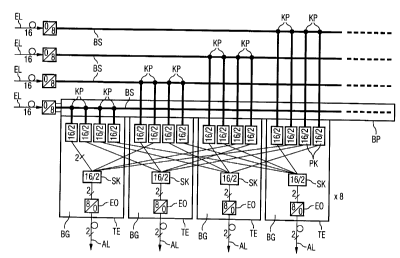
As ca.n be seen from Fig. 1, four harnesses, each having 15
input lines EL are connected on the input side to the
_g_
CA 02338236 2001-O1-19
JINN-18-O1 09:56 p.11 R-501 Job-6T8
Jan.l8. 2001 11:13AM No.9834 P. 11
illustrated switching matrix. The number of input lines EL in
each harness ,is represented by the number 16 in Fig. 1. The
input lines are each in the form of a glass--fiber cable, which
ends at an optica~./electrical converter OE. 64
optic:al/electrical converters 4E are provided, corresponding
to tree total number of 64 input lines, by which converters the
optical input signals are converted into electrical input
signals and are passed to in each case one of the four bus
structures BS, which are each arranged on a separate base
board BP. The base boards BP~ of which only one is illustrated
in Fi_g. 1, are also fitted With the respective 16
optic:al/electrical converters, which are connected on the
input: side to the busy structure BS, in addition to the
respective bus structure BS. The bus structures BS each have
nodes KP, to wh~.ch the line connections between the
optical/electrical converters OE and the respective primary
switching elements PK connected by the bus structure are
cC~nne~cted. Only four of the nodes KP of the bus structures HS
are p_llustrated for each bus structure BS in Fig. 1. The bus
structures HS continue on the right-hand Bide of Fig. 1,
howe~rer, as is represented by the four dashed lines. Further
nodes KP for each bus etz~uature HS are located there.
Likewise, there are line connections tizere from the nodes KP
to the primary switching elements KP, to be precise in each
case 7 x 4 of the primary switching elements PK per bus
atrucaure with, as can be seen from the illustration in Fig.
1, in each case four of the primary switching elements PK
being supported by a common supporting element TE. Overall,
therE: are thus 32 such supporting elements TE, each having
four primary switching elements PK, as can also be seen by the
illu~~tration of the four supporting elements TE which are
shown and by the designation "x 8" in the lower right-hand
part of Fig. 2.
-10-
CA 02338236 2001-O1-19
JAN-16-O1 09:56 P.12 R-501 Job-6T6
an.l8. 2001 11:13AM No.9834 F. 12
Although this cannot be seen from the illustration, the base
boards HP are arranged with the bus structures BS in a row one
above the other, with the large-area base boards being
arranged as subelements of a rear wall of a drawer or of a
rack for accommodating electrical circuits. The rack is, in
particular, a so-called 19" rack, ae is commercially
available. Eight plug-in slots per base board are in each case
located alongside one another on the front face of the base
boards BP and axe occupied by the respective assemblies HG
l0 that are connea>~ed by the bus structure. Further plug-in slots
are provided in order to upgrade the 64/64 switching matrix.
The existing assemblies HG are connected to the associated bus
etruc~ture HS via plug connectors in the plug-in slots, with
the plug connectors each representing a retaining connection
between the base board BP and the supporting element TE. The
supporting elements TE are produced from board material and
are arranged such that the narrow end surfaces of the
supporting elements TE extend in the vertical direction. The
term end surfaces in this case means the end surfaces of the
supporting elements TE, which have a width which corresponds
to the board thickness and have a length which aorresponde to
the shorter outer edge of the rectangle, and is illustrated by
the supporting element TE zn Fig. 1. The longex rectangle
edges and the long narrow surfaces of the supporting elements
2S T1~ e:xtend in the horizontal direction from the respective base
board BP to the fxont face of the 19" rack. They are in this
case each gripped by a guide profile, which makes it easier to
insert and remove the respective supporting elements into its
plug-in slot and from its plug-in slot. Of the total of eight
aaBemblies HG per bus structure BS, only one ie in each case
illustrated in Fig. 1.
Apart from the four przmary switching elements PK, each of the
assemblies BG has a secondary awitchin_y element SK and two
_11_
CA 02338236 2001-O1-19
JAN-18-01 09:56 P 13 R-501 Job-6T8
~an.l8. 2001 11:13AM No.9834 P. 13
elect~rical/optical converters EO which are connected on the
output side to the 9eeondary switching element SK. The output
signals from the respective assemblies HG are converted into
optic:al signals in the electrical/optical converters EO, and
S are passed to the output lines AL. Each assembly BG has two
output lines AL, as is represented by the number 2 in the
signal propagation direction both before and after the
electrical/optical converters EO. The secondary switching
element SK in each case acts as an interface between primary
swit=ching elements PK and the output lines AL or the
electrical/optical converters EO. In the same way as the
primary switching elements PK, the secondary switching
elements SK are also 16/2 switching elements, that ie to say
they each have 16 input ports and two output ports. Of the 16
I5 input. ports of the primary switching elements PK, all are in
each occupied, that is to say are connected >~o in each case
one of the input lines which are connected to the
corre=sponding bus structure HS. The line connections of the
bus E,tructure BS which are illustrated in Fig. 1 should thus
be re=garded as line connections having at least 16 individual
linear or conductor tracks. Digital data can be transmitted,
for example, at a data rate of 800 Mbit/e via each of the
indiv-idual lines or conductor tracks.
The four assemblies BG illustrated in Fig. 1 are networked to
form a funnel structure, in that the output ports o~ in each
case three of the four primary switching elements PK of an
assembly BG are connected to input ports of the secondary
switching elements SK of the three other assemblies HG in the
funnel structure. In this case, the two output ports of a
primary switching element PK are in each case connected to two
of the input ports of the same secondary switching element SK.
In consequence, there are connECtions for each secondary
switching element SK in the funnel structure between the
-12-
CA 02338236 2001-O1-19
JAN-16-O1 09:56 P 14 R-501 Job-676
~a~.?8. 201 1':?4AM No.9834 F. ?4
primary switching elements PK of each assembly HG in the
funnel structure. The actual coupling of the input lines EL in
different input cable harnesses is thus caused out only after
the primary switching elements PK, in the signal propagation
direction, by means of point-to-point connections between the
iridi~~ridual assemblies 1:3G in the funnel_ structures. The
exemplary embodiment in this case ensures that, irrespective
of wJzich of the input lines EL a signal. arrives on at the
switching matrix, the input signal can be passed to any of the
output lines AL of the funnel structure, with the switching
elements PK, SK using the information in the header of an ATM
cell which represents an input signal or a part of an input
signal to identify whether the ATM ce7_1 may be passed to the
respmctive switching element )~K, SK on the output aide.
For cost reasons, 16/2 switching elements are used as the
secondary switching elements SK in the exemplary embodiment
illustrated in Fig. 1, although only eight input port$ of the
secondary switching elements SK are in each case occupied.
Fiowewer, 8/2 switching elements are used in an alternatrive
refinement.
-13-
CA 02338236 2001-O1-19