Note: Descriptions are shown in the official language in which they were submitted.
CA 02338479 2001-02-27
r Y
GOVERNMENT RIGHTS
The United States Government may have certain rights in the
present invention pursuant to Contract No. N00014-96-0291
awarded by the Office of Naval Research.
FIELD OF THE INVENTION
The present invention relates in general to lithography used
in the manufacture of semiconductor devices, and particularly to
an alignment system.
~BACRGROUND OF THE INVENTION
The manufacture of semiconductor devices uses a lithographic
technique. It is often necessary to align or locate an object
with a known reference coordinate system. In microcircuit
lithography, the image of a reticle is projected onto a
CA 02338479 2001-02-27
SVG-4029
photosensitive substrate or wafer which is reproduced forming
circuit patterns. Different processing steps often require
different layers to be sequentially formed on the substrate to
form a semiconductor device. Accordingly, it is often necessary
to relocate the substrate with a high degree of accuracy. The
substrate must be accurately positioned relative to prior
patterns formed thereon. Alignment accuracy is often critical and
typically is required to be less than 0.1 micron. Generally, an
alignment mark or target is placed on a substrate to be aligned
and is located with reference to a second object such as an
alignment sensor. The position of the alignment mark, and
therefore the substrate, is determined with respect to the
alignment sensor coordinates. This is a critical step in
alignment. The position of an alignment mark is normally defined
with respect to the wafer plane and the center of symmetry of
some portion of the alignment mark pattern. Typically an
alignment sensor has an alignment axis that is normal to the
plane of the substrate or wafer. Generally, alignment sensors
require the use of a special alignment mark pattern, or a
relatively restricted class of alignment mark patterns, that is
placed on a substrate or wafer.
An alignment system is disclosed in United States Patent
5,477,057 entitled "Off Axis Alignment System For Scanning
2
CA 02338479 2001-02-27
SVG-4029
Photolithography" issuing to David Angeley et al on December 19,
1995, which is herein incorporated by reference. Therein
disclosed is an alignment system having multiple detectors for
detection of light scattered and reflected from alignment marks
placed on a wafer. Another alignment system is disclosed in
United States Patent 5,559,601 entitled "Mask And Wafer
Diffraction Grating Alignment System Wherein The Diffracted Light
Beams Return Substantially Along An Incident Angle" issuing to
Gallatin et al on September 24, 1996, which is herein
incorporated by reference. Therein disclosed is a grating-grating
interferometric wafer alignment system utilizing a coherent
illumination for determining alignment from the return
electromagnetic radiation intensity. Another alignment system is
disclosed in United States Patent 5,767,523 entitled "Multiple
Detector Alignment System For Photolithography" issuing to
McCullough on June 16, 1998, which is herein incorporated by
reference. Therein disclosed is a detector having a
photosensitive surface covered with an opaque layer having
predetermined openings therein combined with a matched reticle
having predetermined apertures.
While these and other alignment systems have performed
adequately for their intended purpose, there is an increasing
need for improving the accuracy of alignment systems.
3
CA 02338479 2001-02-27
SVG-4029
Additionally, there is a need for an alignment system that can
utilize a relatively large class of alignment mark patterns.
SUMMARY OF THE INVENTION
The present invention is an alignment sensor that is self
referencing to the center of symmetry of any mark having one
hundred and eighty degree symmetry. An alignment mark having one
hundred and eighty degree symmetry placed on the substrate is
illuminated with coherent illumination. The image of the
alignment mark is divided into two images. The images are rotated
one hundred and eighty degree with respect to each other, and are
coherently recombined with an interferometer. With proper phasing
of the interferometer paths the recombined image will interfere
constructively or destructively in amplitude in a detectable and
identifiable way or combine to form detectable and identifiable
polarization states when the axis of the alignment sensor is
located at the center of the alignment mark symmetry. The
alignment mark may be any class of mark having 180° symmetry,
such as alternating spaces and lines, a grid pattern, or a
checkerboard pattern, including other symmetrical patterns.
Preferably, a prism is used to form the two images, rotate the
two images with respect to each other, and interferometrically
4
CA 02338479 2001-02-27
SVG-4029
recombine the two images. A detector detects the interference as
a result of the recombined two images and locates the center of
the alignment mark to accurately detect the position of the
substrate.
Accordingly, it is an object of the present invention to
provide improved alignment in a lithographic system used in the
manufacture of semiconductor devices.
It is an advantage of the present invention that a mark
having one hundred and eighty degree symmetry is used.
It is a feature of the present invention that two images of
the alignment mark are coherently recombined in an interferometer
to accurately identify the center of the alignment mark.
It is a feature of the present invention that a prism is
used to divide, rotate, and recombine the image of an alignment
mark having one hundred and eighty degree symmetry.
These and other objects, advantages, and features will
become readily apparent in view of the following detailed
description.
BRIEF DESCRIPTION OF THE DRAWINGS
Fig. 1 schematically illustrates the alignment sensor of the
present invention.
CA 02338479 2001-02-27
SVG-4029
Figs. 2A-E are plan views illustrating different alignment
marks having one hundred and eighty degree symmetry.
Figs. 3A-E are plan views illustrating the dividing,
rotating, and recombining of an image.
Fig. 4A is a plan view illustrating scanning of an alignment
mark.
Fig. 4B is a graph illustrating an alignment signal and the
identifying of a center of the alignment mark.
Fig. 5A is a schematic illustration of a preferred
embodiment of the present invention.
Fig. 5B is a cross section taken along line 5B-5B in Fig.
5A.
Fig. 6A is the side view of a prism utilized in one
embodiment of the present invention.
Fig. 6B is a top view of the prism illustrated in Fig. 6A.
Fig. 6C is a bottom view of a prism illustrated in Fig. 6A.
Fig. 7A is a side view of a prism of a second embodiment of
the present invention.
Fig. 7B is a top view of the prism illustrated in Fig. 7A.
Fig. 7C is a bottom view of the prism illustrated in Fig.
7A.
Fig. 7D represents a coordinate system.
6
CA 02338479 2001-02-27
SVG-4029
Fig. 8A is a side view of a prism utilized in a third
embodiment of the present invention.
Fig. 8B is a side view of the prism illustrated in Fig. 8A.
Fig. 8C is a bottom view of the prism illustrated in Fig.
SA.
Fig. 9 is a block diagram illustrating the method steps of
the present invention.
DETAILED DESCRIPTION OF THE PREFERRED EMBODIMENTS
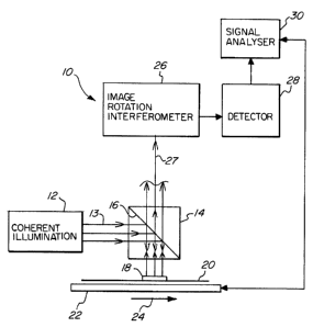
Fig. 1 is a schematic diagram illustrating the present
invention. Alignment sensor 10 comprises a coherent illumination
source 12, such as a laser, providing electromagnetic radiation
13, to a beamsplitter 14. A portion of the electromagnetic
radiation is reflected off coating 16 to illuminate an alignment
mark or target 18. The alignment mark or target 18 has one
hundred and eighty degree symmetry. By one hundred and eighty
degree symmetry, it is meant that when the alignment mark or
target 18 is rotated one hundred and eighty degree about an axis
of symmetry perpendicular to the plane of the alignment mark 18,
the alignment mark is substantially identical to the unrotated
alignment mark. The axis for which this is true is called the
axis of symmetry. The alignment mark 18 is placed on or within a
7
CA 02338479 2001-02-27
SVG-4029
photosensitive substrate or wafer 20. The photosensitive
substrate 20 is placed on a stage 22. The stage 22 may be scanned
in the direction indicated by arrow 24. Electromagnetic radiation
reflected from the alignment mark 18 passes through the
beamsplitter 14 and is collected by the image rotation
interferometer 26. It should be appreciated that a good quality
image need not be formed, but that the features of the alignment
mark should be resolved. The image rotation interferometer 26 may
be any appropriate set of optical elements, and is preferably a
combination of prisms, that form two images of the alignment
mark, rotate one of the images with respect to the other one
hundred and eighty degrees and then recombines the two images
interferometrically so that when aligned with the alignment
target 18, the electromagnetic radiation will interfere either in
a polarization sense or in an amplitude sense, constructively or
destructively, making readily detectable the center of the
alignment mark 18. The optical ray passing through the center of
rotation established by the interferometer, 26, defines the
sensor alignment axis 27. Detectors 28 receive the
electromagnetic radiation from the image rotation interferometer
26. The detectors 28 then provide signals to the signal analyzer
30. The signal analyzer 30 is coupled to the stage 22 such that
the position of the stage is known when the center of alignment
8
CA 02338479 2001-02-27
SVG-4029
mark 18 is determined. Therefore, the position of the alignment
mark 18 is very accurately known with reference to the stage 22.
Alternatively, the location of the alignment sensor 10 may be
known such that the center of the alignment mark 18 is known with
reference to the alignment sensor 10. Accordingly, the exact
location of the center of the alignment target 18 is known
relative to a reference position. Thereby, by using an alignment
mark of a class that is one hundred and eighty degree symmetrical
in combination with an image rotation interferometer, the
alignment system is self referencing to the center of the
alignment mark. This makes possible the use of a wide variety of
alignment marks that need only be one hundred and eighty degree
symmetrical. Additionally, the center of the mark may be very
accurately determined even with a relatively poor image.
Figs. 2A-E are plan views of examples of different possible
alignment marks. It should be appreciated that Figs. 2A-E are
only examples of different alignment marks and that many
different one hundred and eighty degree symmetrical alignment
marks may be utilized in practicing the present invention that
can readily be determined by one skilled in the art based on the
teachings of the present invention. Fig. 2A illustrates a square
grid checkerboard alignment target 18A. The target 18A is
comprised of a plurality of two types of optically different
9
CA 02338479 2001-02-27
SVG-4029
squares, 34 and 36. The two types of squares may be
differentiated by pattern, reflectance (amplitude and/or phase),
or any combination of these. Alignment mark 18A functions
primarily like two linear gratings oriented at right angles with
respect to each other; one at an angle of +45 degrees with
respect to the orientation of edge or line 32 and the other at an
angle of -45 degrees with respect to edge or line 32.
Alignment mark 18A, when rotated one hundred and eighty
degree about an axis perpendicular to its plane results in a
substantially identical pattern or mark. Therefore, alignment
mark 18A is one hundred and eighty degree symmetrical.
Fig. 2B illustrates a diamond shaped alignment mark 18B.
The alignment mark 18B is comprised of a plurality of vertical
equally spaced lines 40 having spaces 38 there between. When the
alignment mark 18B is rotated one hundred and eighty degree about
an axis perpendicular to the plane of the alignment mark 18B, a
substantially identical pattern or mark is formed. Therefore,
alignment mark 18B is one hundred and eighty degree symmetrical.
Fig. 2C illustrates another alignment mark 18C. The
alignment mark 18C has a plurality of lines 44 separated by
spaces 42. The spaces 42 are of different spacing or dimensions.
Therefore, the lines 44 have a different pitch or period. The
different periods of lines 44 are symmetrical about a central
CA 02338479 2001-02-27
SVG-4029
line 46. Therefore, when the alignment target 18C is rotated one
hundred and eighty degree about an axis perpendicular to the
plane of the alignment mark 18C, a substantially identical
pattern or mark is formed. Therefore, alignment mark 18C is one
hundred and eighty degree symmetrical.
Fig. 2D illustrates another alignment target 18D. Alignment
target 18D has alternating lines, which may be spaces 39 and
lands 41. The spaces 39 and the lands 41 are angled forty-five
degrees with respect to the longitudinal axis of the alignment
target 18D.
Fig. 2E illustrates another alignment target 18E. Alignment
target 18E has alternating lines, which may be spaces 45 and
lands 43. The spaces 45 and the lands 43 are angled forty-five
degrees with respect to the longitudinal axis of the alignment
target 18E.
Figs. 3A-E illustrates the image manipulation of the
alignment sensor of the present invention, and in particular the
image rotation interferometer 26, illustrated in Fig. 1. Fig. 3A
illustrates the formation of an image 48. For illustrative
purposes, the image has been selected as the letter F. However,
it should be appreciated in practicing the present invention that
the image of a one hundred and eighty degree symmetrical
alignment mark would be formed. The letter F is not a one hundred
11
CA 02338479 2001-02-27
SVG-4029
and eighty degree symmetrical mark. Fig. 3B illustrates the
formation of two images 48a' and 48b' of the image 48,
illustrated in Fig. 3A. Fig. 3C illustrates rotating one of the
images 48a' or 48b', illustrated in Fig. 3B, with respect to the
other image forming a one hundred and eighty degree rotated image
48" . Fig. 3D illustrates the recombining of image 48a' and image
48" , which is rotated one hundred and eighty degrees illustrated
in Fig. 3C to form an interferometrically recombined image 48" '.
Fig. 3E illustrates the recombining of the left image 48a' of
Fig. 3B when it is rotated +90 degrees and right image 48b' of
Fig. 3B when it is rotated -90 degrees to form an
interferometrically recombined image 48" " . Because the
alignment mark is one hundred and eighty degree symmetrical, the
recombined image will interfere constructively or destructively
when the axis of the alignment sensor is exactly over the
alignment mark center of symmetry. This results in accurate
detection and therefore location of the center of the alignment
mark. It should be appreciated that the optical manipulation of
the image of an alignment mark may be performed in a number of
different equivalent ways. It is only the end result of forming a
first image of the alignment mark and a second image of the
alignment mark rotated one hundred and eighty degrees relative to
the first image that is essential. For example, if two images are
12
CA 02338479 2001-02-27
SVG-4029
formed both images could be rotated ninety degrees in opposite
directions to form the required two images rotated one hundred
and eighty degrees with~respect to each other.
Fig. 4A-B illustrates the application of the present
invention to a scanning sensor or wafer which could be part of a
scanning photolithographic system. In Fig. 4A coherent
illumination 112 scans an alignment target 118 comprised of
vertical lines 136 and spaces 137. Arrow 124 indicates the
relative direction of scan. Generally, the illumination 112 will
be stationary and the alignment target 118 will move relative
thereto. Fig. 4B is a graph illustrating energy as a function of
time. Curve 150 represents a signal obtained by a scanning
alignment system of the present invention. The signal 150 is
contained by an envelope function 152. Point 154 represents the
maximum energy or height of the envelope function 152. This
maximum height or point 154 occurs at a time to representative of
the coincidence of the mark center and the sensor alignment axis
27, illustrated in Fig. 1.
Fig. 5A-B illustrates in more detail an embodiment of the
present invention. The alignment sensor 210 receives coherent
electromagnetic radiation from a source, not illustrated, from a
single-mode polarization-preserving optical fiber 213A. The
optical fiber 213A may transmit two wavelengths of
13
CA 02338479 2001-02-27
SVG-4029
electromagnetic radiation, preferably at 635 and 680 nanometers.
Another single-mode polarization-preserving optical fiber 213B
may be utilized for transmitting three longer wavelengths,
preferably at 780, 830, and 880 nanometers. Fiberoptic couplers
215A and 215B, respectively, may be used to collimate the output
of the optical fibers 213A and 213B to enter a lossless
wavelength based beam combiner cube 217. However, it is possible
to combine the two optical fibers 213A and 213B with a single
optical fiber, eliminating the need for the beam combiner cube
217. The wavelengths should have S-polarization, linear
polarization perpendicular to the plane of the page. Adjacent to
the beam combining cube 217 is a lens 219. Lens 219 provides
illumination pupil correction. Line 221 represents the location
of the corrected pupil plane, which is adjacent to stop 223. The
stop 223 is preferably a square, but may have other shapes such
as a circle, or diamond. Lenses 219, 225, and 231 are selected
and spaced along with pupil plane 221 to provide a nominally
constant phase and uniformly illuminated image of stop 223 at the
substrate plane or wafer 233 having an alignment target 218
thereon. These imaging conditions do not need to be met exactly
for the sensor to function properly. The most critical
requirement is the maintenance of one hundred and eighty-degree
symmetry about the interferometer-defined alignment axis.
14
CA 02338479 2001-02-27
SVG-4029
Optional stop 227 may be used to limit the diameter of lens 225
thereby limiting the substrate illumination numerical aperture to
a predetermined value, preferably approximately 0.2.
An achromatic polarization-based beamsplitter cube 214 is
used to reflect the incident S-polarized illumination toward the
substrate 233 and transmits P-polarization illumination from the
substrate 233 toward a rotation interferometer prism 226. An
achromatic quarter wave plate 229 is placed adjacent to the
beamsplitter cube 214 to convert the incident linear S-
polarization into right or left circularly polarized light
illuminating the wafer mark or alignment target 218. Although not
required, it is useful here to consider the alignment target 218
to be of the form of the checkerboard grating 18A shown in Fig.
2A with the horizontal and vertical lines parallel and normal to
the page. Thus, the checkerboard gratings are oriented at ~45
degrees with respect to the page. The most desirable alignment
mark scan direction is parallel to either the horizontal or
vertical lines. Achromatic quarter waveplate 229 also converts
the desired portion of the substrate-scattered light, including
the non-diffracted zero-order, into the linear P-polarized light
that is transmitted by the beamsplitter 214. An achromatic half-
wave waveplate 235 may be placed adjacent to the beamsplitter
cube 214 in lieu of rotating the rotation interferometer 226
CA 02338479 2001-02-27
SVG-4029
forty-five degrees about the axis of lens 231. The rotation
interferometer 226 is a plurality of prisms combined to
effectively provide two images of the alignment target 218,
rotate one image one hundred and eighty degree with respect to
the other, and interferometrically recombine the images. The
rotation interferometer 226 may be polarization based. Typically,
the rotation interferometer 226 can have a rotation error of
approximately ~ five milli-radians. Typically, the optical path
difference between the two arms should be less than two waves.
Typically, the phase difference between the S and P polarization
reflections should be less than ~ ten degrees. The alignment axis
is defined by interferometer 226 centerline ray 226A and 226B and
the extension of this ray as it propagates throughout the sensor
optics. Ray 226C is the alignment axis extended to wafer target
218. Adjacent to the rotation interferometer 226 is chromatic
wave-plate assembly 237. Chromatic wave-plate assembly 237 is
designed and adjusted to compensate for any small phase errors or
path difference between the two paths within the rotation
interferometer 226. Waveplate assembly 237 can be placed at
either the entrance or exist of the interferometer. Dashed line
239 represents a plane that separates the alignment system 210
into two groups. Prior to this plane, the optical components just
described generate the optical position signals. The components
16
CA 02338479 2001-02-27
SVG-4029
beyond this plane separate the signals and the first order
intensities.
Adjacent to plane 239 is positioned a relay comprising two
lenses 241 and 245. These lenses are selected and spaced to
simultaneously image wafer plane 233 onto plane 243 and pupil
plane 221 onto planes 244 and 255. There is an intermediate image
of pupil plane 221 which is typically located between plane 230
and plane 236 or 239. An optional stop, with a clear region that
is the nominal size of the image of the wafer plane illumination
spot, can be placed in plane 243 to block undesired stray light.
In addition, an optional stop can be placed in plane 244 to
reject undesired stray light, to block undiffracted light, or to
select desired portions of the diffracted light. Adjacent to lens
245 are beamsplitter cubes 247A and 247B. Beamsplitter cubes 247A
and 247B are polarization based mostly transmitting beamsplitter
cubes that transmit all of the local P-polarization while
reflecting approximately five to ten percent of the S-
polarization and transmitting the balance of the S-polarization.
The beamsplitter cubes 247A and 247B are oriented with respect to
interferometer 226 and rotated 90° with respect to the other so
that the final light transmitted has the same polarization state
as the light incident upon beamsplitter 247A. Output light 228A
comes entirely from one path within interferometer 226 and output
17
CA 02338479 2001-02-27
SVG-4029
light 228B comes entirely to the other path within interferometer
226. Following beamsplitter cube 247B is achromatic half-wave
waveplate 249, which is~oriented to rotate the transmitted
polarization forty-five degrees. Following waveplate 249 is
achromatic polarization based beamsplitter cube 251A.
Alternatively, waveplate 249 can be omitted if beamsplitter 251A
and the subsequent components are rotated either ~45 degrees
about alignment axis 226B. Beamsplitter cube 251A serves as an
analyzer for polarization based rotation interferometer 226
generating two complementary alignment signals. One output is
proportional to the sum of the two image fields. The other output
is proportional to the difference between the two fields. The
beamsplitter cube 251A reflects S-polarization illumination
upward along pate 228C and transmits P-polarization. With proper
optical tolerances and wave plate orientations, the wafer or
substrate zero order will be S-polarized and hence exits
beamsplitter 251A along with the alignment position signal pair
that is complementary to the transmitted signals. A detector
assembly 228 is positioned beyond the plane 228'. Detector
assembly 228 includes an achromatic polarization-based
beamsplitter cube 251B. The beamsplitter cube 251B is used in
conjunction with a quarter wave plate 253 and a mirrored stop
255. Beamsplitter cube 251B transmits the incident P-polarization
18
CA 02338479 2001-02-27
SVG-4029
through quarter wave plate 253. Mirror stop 255 is located in an
image of plane 244 and is a mirror with clear areas that transmit
diffraction for the alignment mark gratings oriented at +45
degrees to the page and reflects diffraction for the alignment
mark gratings oriented at -45 degrees to the page. Typically, the
transmitted and reflected diffraction will be both first-order
diffraction orders associated with each grating's orientation
although only one of the diffraction orders is required. One
signal, pair of diffraction orders, is transmitted through mirror
stop 255. The other signal, pair of diffraction orders, is
reflected from mirror stop 255 and travels back through quarter-
wave waveplate 253 for the second time so that it is converted
into S-polarized light and reflected upward by beamsplitter 251B.
Collection lenses 257A and 2578 collect the alignment signal
position light typically forming a third image of the alignment
mark 218 at collector stops 259A and 2598, respectively. The
signal is transmitted by multi-mode optical fibers 261A and 2618,
respectively. Photodetectors are positioned at outputs 263A and
2638 providing the basic alignment position signals. The optics
and detectors following plane 228' can be duplicated at 228C to
provide complementary signals. Either or both complementary
signal pairs can be used. This requires either two or four
photodetectors.
19
CA 02338479 2001-02-27
SVG-4029
The optics and detectors following plane 228' can be
duplicated with beamsplitter 251A replaced by solid glass cube
at both 228A and 228B cxeating two output channels. In each
channel mirror stop 255 is replaced by a modified mirror stop
that selects one of the two incident first orders, transmitting
one and reflecting the other. This requires four photodetectors.
These four signals will give information about the alignment
mark and in particular about mark symmetry. The inclusion and
use of these optics and signals at beamsplitters 247A and 247B
are optional. It should be appreciated that the use of wave-
plates including 235, 249, as well as others may be optional,
depending upon the use of polarization beamsplitters and the
relative orientation of polarization sensitive components.
If several different illumination wavelengths illuminate
mark 218, the signals from each wavelength may be separated at
any point after the mark. A particularly convenient wavelength
separation region is the multimode fibers 261A and 261B just
before the photodetectors positioned at outputs 261A and 261B.
Then there should be an additional set of photodetectors for
each wavelength.
While the embodiment illustrated in Fig. 5A has eight
outputs, four outputs comprising the two complementary pairs of
alignment positions signals generated by interfering opposing
CA 02338479 2001-02-27
SVG-4029
first orders and four outputs comprising four first order
diffraction amplitudes, all outputs are not likely to be needed.
It is estimated that only two outputs may actually be needed.
Fig. 5B is a cross section taken along line 5B-5B in Fig.
5A. The electromagnetic radiation enters the rotation
interferometer 226 at 231'. The electromagnetic radiation exits
the rotation interferometer 226 through wave plate 237 and relay
lens 241.
Figs. 6A-C illustrate different views of the rotation
interferometer 226 illustrated in Figs. 5A and 5B. The prism
configuration of the rotation interferometer 226 is of the Mach-
Zehnder type. This interferometer can be constructed from two
prisms joined at beamsplitter surface BS6. Optical ray path:
in6-a6-b6-c6-ds-e6-out6 and path: in6-a6-bs' -c6' -ds' -e6-out6 define
the interferometer alignment axis. Each letter callout dot
represents a reflection point or beamsplitter BS intersection
point of the alignment axis centerline. Approximately, one-half
of the energy follows each path. The reflections at bs-cb-ds and
b6' -c6' -ds' reflect the associated rays out of the plane of the
figure. Observed along the output ray e6-outs, these out-of-plane
reflections rotate an image plane perpendicular to the ray.
Because the orientation of the two mirrors associated with the
reflections at b6 and d6 are reversed with respect to the
21
CA 02338479 2001-02-27
- ~ SVG-4029
orientation of the two mirrors associated with the reflections at
b6' and d6', the images associated with the two paths are rotated
in opposite directions._The mirror angles are selected so that
the relative image rotation is one hundred and eighty degrees.
The set of desired mirror angles is not unique. The set of
symmetric mirror angles shown is particularly convenient. This
set of angles is unique. This set of angles is described in
detail with respect to Fig. 7A-D. Beamsplitter and mirror
coatings must be designed to control the relative phase shift
between the two interferometer paths to maintain proper
constructive and destructive interference between the two rotated
images. One useful coating solution follows. Use identical
reflective coatings on the four mirrors reflecting at b6, d6, b6',
and d6'. Use metallic type coatings with negligible phase shift
between S-polarization and P-polarization states on the two
mirrors reflecting at c6 and c6'. Use a symmetric coating for
beamsplitter surface BS6.
This interferometer is particularly useful because no light
can return toward the input direction, even with small
fabrication errors.
Fig. 7A-D illustrate different views of another type or
embodiment of a rotation interferometer 326. Rotation
interferometer 326 has an interferometer configuration of the
22
CA 02338479 2001-02-27
SVG-4029
Sagnac ring type. This interferometer can be conveniently
constructed from the three prisms shown. The prisms are joined at
beamsplitter surface BS,.and the surface defined by HW1 and HW2.
The coincidence of the overlap region a,-out, from optical ray
path: in,-a,-b,-c,-d,-e,-a,-out, and path: in,-a,-e,-d,-c,-b,-a,-out,
define the interferometer alignment axis. Each letter callout dot
represents a reflection point or beamsplitter BS, intersection
point. Approximately one-half of the energy follows each path.
The reflections at b,-c,-d, reflect the associated rays out of the
plane of the figure. Observed along the output ray a,-out" these
out-of-plane reflections rotate an image plane perpendicular to
the ray. Because the reversed order of reflection at the out-of-
plane mirrors, b,-c,-d, for the clockwise path and d,-c,-b, for the
counterclockwise path the images associated with the two paths
are rotated in opposite directions. The mirror angles are
selected so that the relative image rotation is one hundred and
eighty degrees. The set of desired mirror angles is not unique.
The set of symmetric mirror angles shown is particularly
convenient. This set of angles is unique. With respect to the
conventional Cartesian unit vectors shown in Fig. 7D, the unit
normal for the mirror reflecting at point b, is:
1 .. 1 ~ 1
2i_2J_~k
23
CA 02338479 2001-02-27
SVG-4029
The unit normal for the mirror reflecting at point d., is:
-~i+~ ~ ~ k
2 2~
The corresponding mirrors in Fig. 6A-6C have similar
orientations. It is preferred if the beamsplitter is
polarization-based, reflecting S-polarization and transmitting P-
polarization. The associated illumination should be coherent with
nominally equal S-polarization and P-polarization energies. With
this equal energy constraint, the interferometer can be designed
to accept any specified elliptical polarization state. It is
preferred to insert a half-wave waveplate at location HW1 or HW2
oriented to rotate the incident polarizations ~90 degrees. For
this preferred configuration, all of the energy leaves the
interferometer form the output face - no light returns toward the
input face. The coatings must be designed with care to insure
proper phase relationships for the S-polarization and P-
polarization associated with the clockwise and counterclockwise
paths to provide the desired constructive and destructive
interference of the two images. In addition to coating design,
proper phase relationship can be established with the use of
polarization sensitive waveplates and coatings external to the
interferometer at either the input or output. The polarization
24
CA 02338479 2001-02-27
SVG-4029
compensator shown at 237, in Fig. 5A, is an example of external
compensation.
This interferometer. is desirable because it is compact,
particularly tolerant of small fabrication errors, and has
inherently equal paths for the two images when coatings are
considered.
Interferometers 226 and 326 can best be understood as
rotating one of the two images one hundred and eighty degrees
with respect to the other image.
Figs. 8A-C illustrate yet another embodiment of a rotation
interferometer 426. The rotation interferometer 426 is another
interferometer of the Mach-Zehnder type. This interferometer is
composed of two beamsplitter cubes BS1 and BS2, two right angle
prisms RPl and RP2, and two pentaprisms PP1 and PP2. Light enters
at ine, and leaves at either both outl and out2 depending upon
the election of mirror and beamsplitter coatings and the addition
of internal waveplates.
It is possible to form another embodiment from a
beamsplitter cube and two Porro prisms. The Porro prisms are
placed on two faces of the beamsplitter cube adjacent to the
beamsplitting surface. The Porro prisms are oriented so that
their central vertices are at ninety degrees to each other.
Polarization and nonpolarization-based configurations can be
CA 02338479 2001-02-27
SVG-4029
designed by the appropriate selection of coatings and the
addition of waveplates. This is an interferometer of the
Michelson type.
Interferometer 426 and the Porro prism based interferometer
can best be understood as providing the desired one hundred and
eighty degree image rotation by performing an x-axis fold of one
of the two images followed by an y-axis fold of either of the
images. This double fold is mathematically identical to rotating
one image 180 degrees with respect to the other.
It should be noted that it is possible to form a one-axis
alignment sensor related to the preceding from an image folded
about its center of symmetry.
All of these different embodiments of rotation
interferometers 226, 326, and 426 form two images of an alignment
mark, rotate one image by one-hundred and eighty degrees relative
to the other image and recombine the two images
interferometrically to determine the center of the alignment
mark. Although less efficient, these interferometers and the
alignment sensor can function with non-polarization-based
beamsplitters.
Fig. 9 is a block diagram illustrating the method steps or
acts of the present invention. Box 510 represents the act or step
of forming two images of a one hundred and eighty-degree
26
CA 02338479 2001-02-27
SVG-4029
symmetrical alignment mark. Box 512 represents the step or act of
rotating one of the two images with respect to the other image.
Box 514 represent the step or act of recombining the two images
in an interferometer. Box 516 represents the step or act of
detecting signals representative of the recombined image. Box 518
represents the step or act of determining the center of the
alignment mark based upon the detected signals.
Referring to Figs. 1-9, the operation of the present
invention should be readily appreciated. The alignment sensor of
the present invention is self referencing to the center of
symmetry of any mark with one-hundred and eighty degrees of
symmetry. One or two dimensional alignment marks, typically
linear gratings and checkerboard gratings, are preferred. The
alignment sensor works from a general interferometric principle
to generate sinusoidal alignment signals. The sensor coherently
divides the coherently illuminated alignment mark image into two
images. One of the images is then rotated one-hundred and eighty
degrees with respect to the other. The images are coherently
recombined and aligned so that the two separate image paths are
substantially exactly equal. The recombined image then interferes
constructively or destructively, in amplitude or in polarization
state depending upon the interferometer configuration, when the
alignment sensor axis is located at the center of the alignment
27
CA 02338479 2001-02-27
' ~ SVG-4029
mark symmetry. With either amplitude or polarization state
interference, two complementary images are formed, one exhibits
constructive interference and is bright, and the other exhibits
destructive interference and is dark or black. The present
invention illuminates an alignment mark with light or
electromagnetic radiation that is spatially coherent with respect
to the same one-hundred and eighty degree symmetry about the
alignment sensor axis. A particularly convenient illumination is
spatially coherent collimated light with a wavefront
perpendicular to the sensor axis and with a centered circular
intensity profile. Alternately, any wavefront with a slight
defocus or radial wavefront aberration may be used. Depending
upon the application, an apodized circular, rectangular, or
square intensity distribution that is smaller or larger in extent
than the alignment mark is useful. The minimum requirement is the
mentioned one-hundred and eighty degree spatially coherence
illumination. Thus, the illumination can be generated from an
extended or spatially incoherent source without discarding most
of the light. The illumination source can contain a continuous
range or several discreet wavelengths. Typically, the light
should be polarized with a state that is symmetric with respect
to the pattern symmetry. For the preferred use of parallel lines
and checkerboards as alignment marks, either left or right
28
CA 02338479 2001-02-27
SVG-4029
circularly polarized light may be used, but other polarization
states are usable. The image quality of the alignment sensor is
not critical as long as one-hundred and eighty degree symmetry is
preserved for each image with proper local interference. Thin
film polarizing beamsplitters may be used. However, they may
require a polarization analyzer to create the two complementary
images. Lossy beamsplitters may also be used. Preferably, a
sequence of beamsplitters and reflections in the form of a solid
glass prism interferometer assembly may be used to provide a
rotation interferometer to separate, rotate, and recombine the
two images. A similar construction is also possible using
diffraction gratings replacing the thin film beamsplitters.
Although not required, it may be useful to spatially filter the
image in order to enhance performance. It is generally useful to
retain the diffracted light, that is light spatially modulated by
the alignment mark pattern, and to reject both the unmodulated
zero-order and randomly scattered light. In addition, it may be
useful to reject higher diffraction orders from periodic marks.
The image can be spatially filtered either before or after the
rotational step. If the illumination underfills a periodic mark
while still illuminating many mark periods, the recombined images
will exhibit maximum constructive or destructive interference
whenever the sensor axis is at a center of the mark symmetry and
29
CA 02338479 2001-02-27
' " SVG-4029
the illumination completely scans the mark. Thus, if a one
dimensional periodic mark pattern moves past the alignment sensor
axis at a constant velocity in the direction normal to the
pattern feature edges, as in a scanning lithographic system,
alignment data is collected. The total energy in each of the
complementary images varies periodically. A particularly
desirable alignment mark is a one dimensional grating composed of
bars in the form of equally spaced lines and spaces. When such a
mark image is spatially filtered to retain only the two first
diffraction orders, the total energy in each of the two
complementary images varies sinusoidally as a function of the
mark position thereby providing a useful alignment signal. The
total energy in one image is of the form: 1+Cos(4~V(t-to)/P)
where V is the wafer stage velocity normal to the pattern lines,
t is time, to is the time at which the center axis at the center
of symmetry of an alignment mark period, and P is the mark
period. The alignment mark sensor position estimate is the mark
location at the time t = to. The complementary image energy is of
the form: 1-Cos(4~V(t-to)/P). The entire signal has a slowly
varying symmetric envelope factor with an increasing and a
decreasing value for its leading and trailing edges, produced as
the alignment mark moves into and then out of the illumination
area respectively. The envelope factor is symmetrical about the
CA 02338479 2001-02-27
SVG-4029
time t = to. For symmetric alignment marks, the alignment signal
and the complementary alignment signal contain the same alignment
information. A two dimensional periodic pattern, such as a
checkerboard grating, can produce simultaneous x-position and y-
position estimates if the recombined image is spatially filtered
and separated into two one-dimensional periodic images with the
energy of each image collected separately. This produces two
independent alignment signals. The positional ambiguity implied
by the periodic nature of a sinusoid can be eliminated by the use
of appropriate pre-alignment precision. Alternately, it can be
eliminated by the use of one or more of the following:
determination of the center of the entire alignment signal
including the envelope factor, the use of two or more periodic
alignment marks of slightly different periods, the use of non-
periodic patterns including isolated features and lines or
checkerboards of variable but symmetrical patterning. Since the
alignment signal does not depend upon conventional image
formation, the alignment sensors will operate over a relatively
large depth of focus. A relative image rotation angle of
approximately one-hundred and eighty degrees is preferable,
although other angles may be used. One image may be folded about
the normal to the alignment sensitive direction providing a
single axis alignment sensor. This folding can be repeated about
31
CA 02338479 2001-02-27
SVG-4029
a second axis to provide alignment information for the other
axis. The required interferometric image manipulation may be
performed in a number of ways in combination with various optical
components. Preferably, the required interferometric image
manipulation of a rotational interferometer is comprised of a
solid glass interferometer prism configuration incorporating
symmetric use of lossless amplitude or polarization sensitive
beamsplitters and symmetric out-of-plane reflections from plane
mirror surfaces.
Figs. 6A-C, 7A-D, and 8A-C illustrate three interferometric
configurations, although others are possible. The designs
illustrated in Figs. 6A-c and 7A-C contain a particularly useful
three mirror geometry in the form of a totally reflecting prism.
There are two mirror surfaces symmetrically placed about a center
base mirror. An image incident into the assembly on one side
exits the second side rotated counterclockwise, that is rotated
plus ninety degrees. An image incident into the assembly on the
second side exits the first side rotated clockwise, that is
rotated minus ninety degrees, so that the two images are rotated
the desired one-hundred and eighty degrees with respect to each
other. The image rotations can be interpreted as three-
dimensional coordinate system rotations. The image manipulation
and interferometric techniques may be assembled from combinations
32
CA 02338479 2001-02-27
SVG-4029
of other equivalent optical elements, such as gratings, Koster's
prisms, lossy beamsplitters, both spherical and cylindrical
lenses, as well as incorporating the reflections from folded
mirror geometries such as corner cubes and ninety degree roof
prisms among others. A practical embodiment may be the use of
solid glass Michaelson interferometer-based configurations with
folded mirror systems, in the form of prisms with internally
reflecting bare or coated surfaces, replacing the usual air
spaced flat mirrors. Two other options may be either one corner
cube mirror assembly and a flat mirror or two ninety-degree roof
prisms oriented with their vertices at right angles. However,
such assemblies present fabrication difficulties and can return
some light back toward the alignment mark. Variations of the
mentioned Michaelson type interferometers have been used in
Fourier transform spectrometers to measure star light coherence.
The present invention can be applied to mask pattern and aerial
image position sensing, as well as non-lithographic applications.
Accordingly, it should be appreciated that the present
invention greatly facilitates alignment and is particularly
applicable to alignment used in lithographic operations in the
manufacture of semiconductor devices. The alignment sensor of the
present invention makes available a large number of different
alignment mark patterns and is self-referencing to the center of
33
CA 02338479 2001-02-27
SVG-4029
symmetry of the alignment marks. Accordingly, although the
preferred embodiment has been illustrated and described, it will
be obvious to those skilled in the art that various modifications
may be made without departing from the spirit and scope of this
invention.
34