Note: Descriptions are shown in the official language in which they were submitted.
CA 02338564 2001-01-24
WO 00/05815 PCTIUS99/14162
SINGLE CHIP CMOS TRANSMITTER/RECEIVER
AND VCO-MIXER STRUCTURE
BACKGROUND OF THE INVENTION
1. Field of the Invention
The present invention relates to a communication system, and in particular, to
a CMOS radio frequency (RF) communication system. The present invention also
relates to a voltage controlled oscillator (VCO) and mixer, and more
particularly, to
a multi-phase VCO and mixer.
2. Background of the Related Art
Presently, a radio frequency (RF) communications system has a variety of
applications including PCS communication and IMT systems. As such, a CMOS chip
integration of the system has been pursued to reduce the cost, size and power
consumption.
Generally, the RF communication system is composed of a RF front-end block
and a base-band digital signal processing (DSP) block. Currently, the base-
band DSP
block can be implemented with low cost and low power CMOS technology.
However, the R.F front-end block cannot be implemented by CMOS technology
because of limitations in speed and noise characteristics, which are below the
speed and
noise specification of popular RF communication systems.
For example, the PCS hand-phone systems operate at a frequency over 2.0
GHz, but current CMOS technology reliably operates only up to approximately
1.0
GHz in terms of speed and noise. Hence, the RF front-end block is implemented
using bipolar or bi-CMOS technology that has better speed and noise
characteristics
than CMOS technology, but is more expensive and consumes more power.
Currently, two different types of RF architecture called "direct conversion"
and
"double conversion" are used for CMOS RF communication systems. Both
architectures have advantages and disadvantages in terms of CMOS
implementations.
1
CA 02338564 2001-01-24
WO 00/05815 PCT/US99/14162
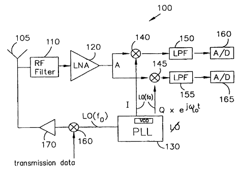
Fig. 1 shows a related art direct conversion CMOS RF communication system
100, including an antenna 105, a RF filter 110, a low noise amplifier (LNA)
120, a first
mixer 140, a second mixer 145, a phase-locked loop (PLL) 130, a first low pass
filter
(LPF) 150, a second LPF 155, a first analog/digital (A/D) converter 160, a
second A/D
converter 165, a third mixer 160 and a power amplifier 170.
The antenna 105 receives RF signals, and the selected RF signals are then
filtered
at the RF filter 110. The filtered RF signals are amplified with a gain at the
LNA 120,
and the RF signals passing through the LNA 120 are directly demodulated into
base
band signals by quadrature multiplication at the first and second mixers 140,
145. The
PLL 130 preferably generates two types of clock signals, I signals and Q
signals, using
a voltage controlled oscillator (VCO). The I clock signals and the Q clock
signals are
the same, excepting a phase difference. I signals preferably have a phase
difference of
90 degrees from Q signals. That is, Q signals are phase shifted with respect
to
quadrature phase shift I signals. The two sets of signals I, Q are preferably
used to
increase the ability of the RF system to identify or maintain received
information
regardless of noise and interference. Sending two types of signals having
different
phases reduces the probability of information loss or change. A demodulation
frequency fo in Figure 1 is equal to a modulation frequency fo.
The demodulated based band signals have a frequency reduced by the frequency
fo from an original frequency to pass through the first and second LPF 150,
155 and
eventually become respective signals required for A/D conversion at the first
and
second A/D converters 160, 165. The digital signals are then transferred to a
base-
band discrete-time signal processing (DSP) block (not shown). Channel
selection is
performed by changing frequency fo in at the phase-locked loop (PLL) 130.
One of the possible causes for the approximately 1 GHz limitation on the
reliability of CMOS technology is the structure of the VCO and the mixer in
the PLL
130. Figure 2 shows a circuit diagram of a background VCO-mixer, wherein the
VCO 10 includes four differential delay cells 12, 14, 16 and 18 and has a
structure
2
CA 02338564 2001-01-24
WO 00/05815 PCTIUS99/14162
similar to a ring oscillator. The four delay cells 12, 14, 16, 18 are serially
connected
and generate a clock signal LO + and an inverted clock signal LO-, each having
a
frequency f, A control circuit for the VCO 10 that generates a frequency
control
signal includes a phase frequency detector 4, a charge pump 6 and a loop
filter 8 that
outputs the frequency control signal to each of the delay cells 12, 14, 16,
18. The phase
frequency detector 4 receives a reference clock signal frel and a VCO clock
signal fvco
from a reference clock divider circuit 2 and a VCO clock divider circuit 3,
respectively.
The frequency f,) of the clock signals LO + and LO- is represented by M/K
(frer)=f,,
Thus, the frequency fo is based on the reference clock signal fr,E and the
divider
circuits 2, 3.
The mixer 20, for example, a Gilbert - Multiplier, multiplies the input
signals,
such as radio frequency (RF) signals RF + and RF-, with the clock signals LO +
and
LO-. The mixer 20 includes two load resistors Rl, R2 coupled to a source
voltage VDD,
eight NMOS transistors 21-28, and a current source IS1. The gates of the NMOS
transistors 21, 22 are coupled to receive the clock signal LO+, and the gates
of the
NMOS transistors 23, 24 are coupled to receive the inverted clock signal LO-.
The
gates of the NMOS transistors 25, 26 receive a common bias voltage VBi, The
gates
of the NMOS transistors 27, 28 receive the RF signals RF+, RF-, respectively.
Therefore, the clock signals LO +, LO- are multiplied with the RF signals RF+,
RF-
only when the transistors 25, 27 or the transistors 26, 28 are transitted to
the "ON"
state together. The output signals OUT+, OUT- of the mixer 20 have a frequency
lower than its original frequency by the frequency f,, of the clock signals LO
+, LO-.
While a wide frequency range and a low phase noise are desirable for various
applications, the VCO-mixer structure 10, 20 can only support up to a
frequency of
approximately 1 GHz with reliable phase noise and frequency range. The
performance of the VCO-mixer structure 10, 20 deteriorates in terms of phase
noise
and frequency range, and is unacceptable as the frequency of the clock signals
LO +,
LO- from the VCO increases. Hence, the VCO 10 and the mixer 20 cannot be
readily
3
CA 02338564 2001-01-24
WO 00/05815 PCT/US99/14162
implemented when the frequency f. of the clock signals LO+, LO- exceeds
approximately 1 GHz.
As described above, the related art direct conversion RF system 100 has
advantages for CMOS RF integration because of its simplicity. In the related
art
direct conversion RF system, only a single PLL is required and high-quality
filters are
not required. However, the related art direct conversion architecture has
disadvantages that make single chip integration difficult or impossible.
As shown in Figure 3A, clock signals cos WI_ot from a local oscillator (LO)
such
as the VCO may leak to either the mixer input or to the antenna, where
radiations
may occur because the local oscillator (LO) is at the same frequency as the RF
carriers.
The unintentionally transmitted clock signals 0(t)cos Wot signals can reflect
off
nearby objects and be "re-received" by the mixer. The low pass filter outputs
a signal
M(t) +A(t) because of leakages of clock signals. As shown in Figure 3B, self-
mixing
with the local oscillator results in problems such as time variations or
"wandering"
DC-offsets at the output of the mixer.
Figure 3B illustrates time variations and a DC-offset. "A" denotes a signal
before the mixer and "B" denotes a signal after the mixer. The time-varying DC-
offset,
together with inherent circuit offsets, significantly reduce the dynamic range
of the
receiver portion. In addition, a direct conversion RF system requires a high-
frequency,
low-phase-noise PLL for channel selection, which is difficult to achieve with
an
integrated CMOS voltage controlled oscillator (VCO), for at least the reasons
discussed
above.
Figure 4 shows a block diagram of a related art RF communication system 300
according to a double conversion architecture that considers all of the
potential
channels and frequency transistors. The RF communication system 300 includes
an
antenna 305, a RF filter 310, a LNA 320, a first mixer 340, a second mixer
345, and a
first LPF 350, a second LPF 355, second stage mixers 370-373, a first adder
374, and a
second adder 375. The RF communication system 300 further includes a third LPF
4
CA 02338564 2001-01-24
WO 00/05815 PCTIUS99/14162
380, a fourth LPF 385, a first A/D converter 390, a second A/D converter 395,
first
and second PLLs 330, 335, a third mixer 360 and a power amplifier 370.
The mixers 340, 345, 370-373 are all for demodulation, while the third mixer
360 is for modulation. The first and second mixers 340, 345 are for a selected
RF
frequency and the second stage mixers 370-373 are selected for an intermediate
frequency (IF). The first PLL 330 generates clock signals at a high frequency
or the RF
frequency, the second PLL 335 generates clock signals having a low frequency
or the
intermediate frequency (IF).
Transmission data are multiplied with the clock signals having the RF
frequency
from the PLL 330 to have a frequency reduced by the RF frequency from an
original
transmission data frequency. The output signals of the third mixer 360 are
amplified
with a gain at the power amplifier 370 and then radiated through the antenna
305 for
transmission.
For reception data, the antenna 305 receives RF signals and the RF filter 310
filters the RF signals. The filtered RF signals are amplified by the LNA 320
and
converted into IF signals by the quadrature mixers 340, 345 with a single
frequency
local oscillator, generally a VCO. The PLL 330 generates clock signals for I
signals and
Q signals of the RF signals. The first mixer 340 multiplies the RF signals
with the
clock signals for the I signals having the RF frequency, and the second mixer
345
multiplies the RF signals with the Q signals having the RF frequency. The LPFs
350,
355 are used at an IF stage (i.e., first stage) to remove any frequency
components not
converted upon conversion to the IF signals, which allows all channels to pass
to the
second stage mixers 370-373. All of the channels at the IF stage are then
frequency-
translated directly to base-band frequency signals by the tunable PLL 335 for
channel
selection.
Demodulated base band signals C pass low pass filters (LPF) 380, 385 and are
converted into digital data by A/D converters 390, 395. The digital data is
then
transferred into a base-band discrete-time signal processing (DSP) block (not
shown).
5
CA 02338564 2001-01-24
WO 00/05815 PCTIUS99/14162
As described above, the related art double conversion RF system 300 has
various
advantages. The related art double conversion RF system 300 performs the
channel
tuning using the lower-frequency, i.e., IF, second PLL 335, but not the high-
frequency,
i.e., RF, first PLL 330. Consequently, the high-frequency RF PLL 330 can be a
fixed-
frequency PLL that can be more effectively optimized. Further, since channel
tuning
is performed with the IF PLL 335, which operates at a lower frequency, the
contribution of phase noise into channel selection can be reduced.
However, the related art double conversion RF system 300 has various
disadvantages. The related art double conversion RF system 300 uses two PLLs,
which
are difficult to integrate in a single chip. Further, the frequency of first
PLL remains
too high to be implemented with CMOS technology, and in particular, with a
CMOS
VCO. The structure of the VCO and mixer imposes an approximately 1 GHz
limitation on the reliability of the CMOS technology. In addition, a self-
mixing
problem still occurs because the second PLL is at the same frequency of the IF
desired
carrier. Figure 5A illustrates leakage of clock signals in the RF
communication system
300, and Figure 5B illustrates time variation and "wandering" DC-offset due to
leaking
clock signals 0(t)cos(,.)LOZ(t) (e.g., self-mixing) in the RF communication
system 300
of Figure 4.
In Figure 5A, the first mixer multiplies the RF signals with clock signals
cos(~)LOIt for RF having a frequency WLOI and outputs the RF signals with
M(t)cos
COLO2t having a frequency reduced by the frequency (L)LOI. The second mixer
multiples
the RF signals from the first mixer with clock signals cosWLO2 for IF having a
frequency wLO2. However, since the frequency of the output signals of the
second
mixer is same as the frequency of desired RF carriers before the LPFs. Thus,
the
output signals of the second mixer may leak to a substrate or may leak to the
second
mixer again. The time-varying DC-offset, together with inherent circuit
offsets,
significantly reduces the dynamic range of the receiver portion.
6
CA 02338564 2008-11-21
WO 00/05815 PCT/US99/14162
SUMMARY OF THE INVENTION
An object of the present invention is to at least substantially obviate
problems
and disadvantages of the related art.
A further object of the present invention is to fabricate a CMOS RF front end
and method for using same that allows one chip integration of an RF
communication
system.
Another object of the present invention is to provide an RF communication
system and method with reduced cost and power requirements.
Still another object of the present invention is to provide a reliable high
speed,
low noise CMOS RF communication system and method for using same.
Another object of the present invention is to increase a frequency range of a
RF
front end of an RF communication system.
A further object of the present invention is to fabricate a VCO-mixer on a
single substrate.
Another object of the present invention is to increase the frequency range of
a
VCO-mixer structure.
Still another object of the present invention is to reduce the noise of a VCO-
mixture structure.
Another object of the present invention is to increase a performance of the
VCO-myiYer structure.
To achieve at least the above objects and advantages in a w hole or in parts
and
in accordance with the purpose of the present invention, as embodied and
broadly
described, the structure of the invention includes a receiving unit that
receives signals,
including selected signals having a carrier frequency, a PLL that generates
multi-phase
7
CA 02338564 2001-01-24
WO 00/05815 PCTIUS99/14162
clock signals having a frequency different from a carrier frequency and a
reference
signal having the carrier frequency, and a demodulation-mixing unit that mixes
the
received signals with the multi-phase clock signals to output the selected
signals having
a frequency reduced by the carrier frequency.
To further achieve the objects in a whole or in parts, in accordance with the
purpose of the present invention, a single chip RF communication system
includes a
transceiver for receiving and transmitting RF signals, a PLL for generating 2N-
phase
clock signals having a frequency 2*f/N smaller than a carrier frequency,
wherein N
is a positive integer as a phase number and fo is the carrier frequency, a
demodulation
mixing unit for mixing the RF signals from the transceiver with 2N-phase clock
signals
from the PLL to output the RF signals having a frequency reduced by the
carrier
frequency and comprising a plurality of two input mixers, and a A/D converting
unit
for converting the RF signals from the demodulation mixing unit into digital
signals.
To still further achieve the objects in a whole or in parts, in accordance
with the
purpose of the present invention, a method of operating a RF communication
system
includes receiving signals including selected signals having a carrier
frequency,
generating multi-phase clock signals having a frequency different from the
carrier
frequency, and a reference signal having the carrier frequency, and mixing the
received
selected signals with the multi-phase clock signals to output the selected
signals having
a frequency reduced by the carrier frequency.
To achieve the advantages and in accordance with the purpose of the present
invention, as embodied and broadly described, the structure of the invention
comprises a clock generator that generates a plurality of first clock signals
having
different phases, each first clock signal having first frequency less than a
reference
frequency, and a mixer coupled to said clock generator for receiving the
plurality of
first clock signals to generate a plurality of second clock signals having a
second
frequency which is substantially same as the reference frequency, wherein said
mixer
8
CA 02338564 2001-01-24
WO 00/05815 PCTIUS99/14162
multiplies the plurality of second clock signals with input signals to provide
output
signals.
Additional advantages, objects, and features of the invention will be set
forth
in part in the description which follows and in part will become apparent to
those
having ordinary skill in the art upon examination of the following or may be
learned
from practice of the invention. The objects and advantages of the invention
may be
realized and attained as particularly pointed out in the appended claims.
BRIEF DESCRIPTION OF THE DRAWINGS
The invention will be described in detail with reference to the following
drawings in which like reference numerals refer to like elements wherein:
Figure 1 is a circuit diagram showing a related art RF communication system;
Figure 2 is a circuit diagram of a related art VCO-mixer structure;
Figure 3A is a diagram showing clock signal leakage in the circuit of Figure
1;
Figure 3B is a diagram showing "self mixing" in the circuit of Figure 3A;
Figure 4 is a circuit diagram showing another related art RF communication
system;
Figure 5A is a diagram showing clock signal leakage in the circuit of Figure
4;
Figure 5B is a diagram showing "self mixing" in the circuit of Figure 5A;
Figure 6 is a diagram showing a first preferred embodiment of a multi-phase,
low frequency (MPLF) RF communication system according to the present
invention;
Figure 7 is a block diagram showing an exemplary PLL circuit;
Figure 8 is a block diagram showing a receive portion of a RF communication
system according to another preferred embodiment of the present invention;
Figure 9 is a block diagram showing the RF communication system of Figure
8 with six phases;
Figure 10 is a block diagram showing a receive portion of a RF communication
system according to yet another preferred embodiment of the present invention;
9
CA 02338564 2001-01-24
WO 00/05815 PCTIUS99/14162
Figure 11 is a block diagram showing the RF communication system of Figure
with six phases;
Figure 12 is a block diagram showing a transmit portion of a RF
communication system according to still yet another preferred embodiment of
the
5 present invention;
Figure 13A is a block diagram showing an exemplary VCO-mixer structure;
Figure 13B is a circuit diagram showing the VCO-mixer structure of Figure
13A;
Figure 14 is a circuit diagram showing another exemplary VCO-mixer; and
10 Figures 15A-15H are diagrams showing operational timing waveforms of Figure
14.
DETAILED DESCRIPTION OF PREFERRED EMBODIMENTS
A single chip radio frequency (RF) communication system formed using CMOS
techniques has various requirements. A CMOS voltage controlled oscillator
(VCO)
has poor noise characteristics. Accordingly, a CMOS phase-locked loop (PLL)
integration is required. However, the number of PLL should be small and the
center
frequency of a PLL preferably differs sufficiently from a transmitting RF
frequency
(e.g., preferably low enough) to control a phase noise result using the CMOS
VCO.
High-quality filters are preferably eliminated because of associated
disadvantageous
area and power specifications. Also, a number of components in the CMOS RF
system should be small or reduced without performance degradation.
A first preferred embodiment of the present invention is a "multi-phase, low
frequency" (MPLF) conversion RF communication system 500 shown in Figure 6 and
can preferably be formed on a single CMOS chip. The first preferred embodiment
can
operate at frequencies well above approximately 1 GHz. The phrase "multi-phase
low
frequency conversion" is used because a single-phase periodic signal having a
high
frequency is preferably obtained by multiplying multi-phase low-frequency
periodic
CA 02338564 2001-01-24
WO 00/05815 PCT/US99/14162
signals. The first preferred embodiment of the MPLF conversion RF
communication
system 500 includes a front-end MPLF RF block 502 and a digital signal
processing
(DSP) block 504, which is preferably base-band. As discussed above, related
art DSP
blocks can be formed of CMOS techniques. Accordingly, a detailed explanation
of the
DSP block 502 including a digital signal processor 550 will be omitted.
The MPLF conversion RF block 502 includes an antenna 505, an RF filter 510
(e.g., band pass filter), a low noise amplifier (LNA) 520 and first and second
mixers
530, 560, respectively. The MPLF conversion RF block 502 further includes a
phase-
locked loop (PLL) 540, a low pass filter (LPF) 580, an analog/digital (A/D)
converter
590 and a power amplifier 570 coupled between the second mixer 560 and the
antenna
505. The PLL 540 generates a modulating and de-modulating clock, i.e., local
oscillator(LO), whose frequency is determined by a reference clock (REF fo).
Figure 7 shows a block diagram of an exemplary embodiment of the PLL 540.
The PLL 540 includes reference and main dividers 610, 620, respectively, a
phase
comparator 630, a loop filter 640 and a voltage controlled oscillator (VCO)
650. The
VCO 650 outputs the LO frequency f,,, which is compared to the reference clock
signal by the phase comparator 630. An output signal of the phase comparator
630 is
passed though the loop filter 640 as a control signal (e.g., frequency) for
the VCO 650.
The frequency of the LO is preferably varied according to the communication
system.
For example, the LO frequency for a personal communication system (PCS) can be
about 1.8 GHz, and the LO frequency for the IMT 2000 system is about 2.0 GHz.
In the first preferred embodiment of the MPLF conversion RF communication
system 500 shown in Figure 6, transmission data is received by the MPLF RF
block
502 from the DSP block 504. The transmission data is modulated by a preferably
modulating second mixer 560 at the LO frequency. The modulated data is
amplified
by the power amplifier 570 and output by the antenna 505.
The low noise amplifier (LNA) 520 receives an input signal from the antenna
505 and amplifies the signal level to output an RF signal. The RF BPF 520 is
11
CA 02338564 2001-01-24
WO 00/05815 PCT/US99/14162
preferably coupled between the antenna 505 and the LNA 520. The RF signal is
de-
modulated by the de-modulating first mixer 530 at preferably the same
frequency as
the modulation frequency. The output of the de-modulating mixer 530 becomes
received data by passing the LPF 580. The received data is preferably
converted to a
digital signal by the A/D converter 590 and output to the DSP 550.
In order to use a single PLL with a center frequency sufficiently lower than a
transmitting RF frequency, the first preferred embodiment of the MPLF
conversion
RF communication system 500 uses a single-phase high-frequency periodic signal
(i.e.,
RF frequency) obtained by multiplying a multi-phase low-frequency periodic
signal
together. In particular, a high frequency "sine" and "cosine" signal is needed
in a RF
system, although the present invention is not intended to be so limited. Sine
and
cosine signals, which have frequencies of WR-F , can be obtained by
multiplying N-phase
sine signals that have frequencies of 2(x)KF/N as shown in equations 1 and 2:
N- (1)
-1
N-1 2 2.W
cos(A) RF=2 2 II sin( FIF.t- 2'k'71 +7t
k=O N N
(2)
N-1
N-1 2 2.CJ
sinw~ 2 2 II sin( ~.t- 2.k ~[
k= o N N
12
CA 02338564 2001-01-24
WO 00/05815 PCTIUS99/14162
A multiplication factor is not "N" but "N/2" because the remaining N/2 sine
signals can be an inverted version of the first N/2 sine signals. The inverted
signals are
preferably used to make differential signals for a differential input mixer.
Figure 8 shows a receive portion 700 of a second preferred embodiment of a RF
block according to the present invention, which can be used in the first
preferred
embodiment of the MPLF conversion RF communication system. The receive portion
700 includes an antenna 715, an RF filter 720, a LNA 725 and a demodulation
mixer
730. The receive portion 700 of the RF block further includes a PLL 740, a low
pass
filter 780 and an analog/digital converter 790. The PLL 740 generates a de-
modulating
clock, i.e., local oscillator (LO) equal to 2'~fo/N, whose frequency is
determined by a
reference clock (not shown). The antenna 715, the RF filter 720, the LNA 725,
the
LPF 780 and the analog/digital converter 790 operate similar to the first
preferred
embodiment, and accordingly, a detailed explanation is omitted.
The receive portion 700 of the RF block uses one PLL 740. The PLL 740 uses
a frequency of 2fo/N, and generates in total 2N-phase clock signals. The PLL
740
generates N-phase LO,os(k,t) and N-phase LOS;,,(k,t) signals, which are
preferably
determined as shown in equations 3-4.
(3)
LOrog(k,t)sin(2wt- 2k7t + n)where,k=0,1,2...N-1
N N N" 2
LOr'j. (k,t)sin(2wT t- 2kn)rvhere,k=0,1,2,...N-1 (4)
N N 2
As shown in Figure 8, the receive portion 700 of the RF block has the
demodulating mixer 730 divided into upper and lower mixer arrays 732, 734.
Each of
the upper and lower mixer arrays 732, 734 includes a plurality of conventional
2-input
13
CA 02338564 2001-01-24
WO 00/05815 PCTIUS99/14162
mixers 735. The upper mixer array 732 multiplies N-phase (N/2: un-inverted,
N/2:
inverted) with a frequency of (26),)/N, sine signals and a RF signal, which is
equivalent to multiplying single phase, frequency of (k), cosine signals and
the RF
signal. Both un-inverted and inverted sine signals are needed for inputting to
a single
mixer because the conventional 2-input mixer requires differential input. The
lower
mixer array 734 multiplies N-phase (N/2 non-inverted, N/2 inverted) with a
frequency
of Wu/N, sine signals and the RF signal, which is equivalent to multiplying
single
phase, frequency of WRF sine signals and the RF signal. Thus, the receive
portion 700
of the RF block functions equivalently with the direct conversion architecture
shown
in Figure 1. However, the receive portion 700 according to the present
invention uses
the N-phase, a frequency of 2w,/N, sine signals in de-modulation in contrast
to the
single phase, and a frequency of W, sine signals.
As described above, the PLL 740 generates 2N-phase clock signals. N-phase
clock signals are N-phase sine signals and N-phase cosine signals. Both the N-
phase
signals includes N/2 non-inverted signals and N/2 inverted signals. The N-
phase sine
signals are input to the upper mixer array 732 together with the RF signals,
and the N-
phase sine signals are input to the lower mixer array 734, together with the
RF signals.
The upper and lower mixer arrays 732 and 734 have a plurality of mixers 735
and a M
number of stages respectively. The M number of stages includes a first stage,
(e.g.,
735), a second stage (e.g., 735 ,),..., a M-lth stage, and a Mth stage (e.g.,
735 "). Each
stage of each mixer array includes at least one mixer having two inputs. The
number
K1 of mixer at the first stage is the highest number of stages. The last
stage, the Mth
stage, has the lowest number (KM) of mixers among the whole stages. The
relative
order of the mixer-number among the stages may be expressed the inequality
K1)K2)K3)K4......KM-1)KM.
Each mixer 735 has two inputs. Each input has an inverted signal and a non-
inverted signal of the inverted signal because each input of the mixers 735
inputs two
different signals. As described above, the RF signals from the LNA 725 and the
N-
14
CA 02338564 2001-01-24
WO 00/05815 PCTIUS99/14162
signals from the PLL 746 are used as the input signals of mixers 735 at a
first stage.
Output signals of mixers 735 at the first stage are used as input signals of
mixers 735 '
at the second stage. In a same manner, output signals of mixers at the M-lth
stage are
used as two input signals of a mixer 735 ", which is a single mixer at the Mth
stage of
the upper mixer array 732 and the lower mixer array 734.
Figure 9 shows a 6-phase example for the receive portion 700 of an MPLF
conversion RF communication system that uses the conventional 2-input mixer. A
PLL 840 generates 12-phase sine signals, which are transmitted to a mixer 830.
The
phase difference between adjacent two signals is 1Z/6 (i.e., 21L/12). Phases
(0,2,4,6,8,10)
are used as inputs to an upper mixer 832 and multiplied together with the
preferably
RF input, which is equivalent with multiplying cos (C),t) and the RF input.
Phases
(1,3,5,7,9,11) are input to a lower mixer 834 and multiplied together with the
preferably RF input, which is equivalent with multiplying sin (W,t) and the RF
input.
Accordingly, the frequency of the clock signals is f. when the clock signals
are
multiplied with the RF signals.
The PLL 840 includes a clock generator such as a voltage controlled source
(VCO) and thus generates 12-phase clock signals for the multiplication with
the RF
signals upon demodulation. The generated clock signals have a frequency 2-
~fo/P
(P=phase number) lower than a frequency fo to be multiplied with the RF
signals.
The clock signals from the PLL 840 may have the lower frequency 2-`fo/P
because the
PLL 840 generates multi-phase clock signals phase 0,....., phase 12. Filtered
RF signals
are amplified with a gain in the LNA 725 and multiplied with the multi-phase
clock
signals, resulting in 12 sine signals in the mixer array 830 for modulation.
The RF
signals multiplied with the clock signals have a frequency lower than an
original
frequency by a final frequency f, of the clock signals.
The initial frequency 2-"fo/P of the clock signals from the PLL 840 is changed
to the frequency fo for multiplication with the RF signals in the mixer (e.g.,
mixer
array) 830. Therefore, the upper mixer array 832 and the lower mixer array 834
CA 02338564 2001-01-24
WO 00/05815 PCT/US99/14162
combine the clock signals having the frequency 2''fo/P and multiply the clock
signals
having frequency f, with the RF signals. Consequently, the RF signals having a
frequency reduced by frequency fo pass through the LPFs 780 and the A/D
converters
790 and are sent to a DSP part (not shown). The 12 phase sine signals
generated by the
PLL 840 are shown as follows:
Phase 0 : sin ( coRFt+ n )
3 6
Phase 1: sin ( WRf t)
3
Phase 2 : sin ( ~RFt- n )
3 6
Phase 3: sin( WRFt-?)
3 6
Phase 4: sin ( CL)RFt- 3n )
3 6
)
Phase 5: sin RF t- 4n
3 6
Phase 6: -sin ( CL)RFt+ n )
3 6
Phase 7: -sin ( WRFt)
3
Phase 8: -sin( wRFt- n)
3 6
16
CA 02338564 2001-01-24
WO 00/05815 PCT/US99/14162
Phase 9: -sin ( WRFt- 211
)
3 6
Phase 10 :-sin ( WRFt- 3n ~
3 6
Phase 11: -sin ( 3f t- 6)
Figure 10 shows a MPLF conversion receive portion 900 of an RF block
according to a third preferred embodiment of the present invention, which can
be used
in the first preferred embodiment of the MPLF conversion RF communication
system.
The receive portion 900 includes an antenna 915, a RF filter 920, a LNA 925
and
mixer 930. The receive portion 900 of the RF block further includes a PLL 940,
a LPF
90 and an A/D converter 990. The PLL 940 preferably generates a de-modulating
clock, i.e., local oscillator (LO) preferably equal to 2'~-fRF/N, whose
frequency is
determined by a reference clock (not shown). The antenna 915, the RF filter
920, the
LNA 925, the LPF 980 and the A/D converter 990 operate similar to the first
preferred embodiment, and accordingly, a detailed explanation is omitted.
The receive portion 900 of the RF block uses just one PLL. The PLL 940
includes a clock generator 942 preferably using a frequency of 2-'-fRF/N. The
clock
generator 942 preferably generates N-phase LO,os(k,t) and N-phase
LOS;,,(k,t)
signals, which total 2N phase signals. The clock generator 942 is preferably a
multi-
phase VCO and the mixing section 930 is also a multi-phase mixer.
As shown in Figure 10, the receive portion 900 of the RF block uses multi-
phase
mixers 932 and 934. The upper multi-phase mixer 932 replaces the function of
the
upper mixer array 732 and the lower multi-phase mixer 934 replaces the
function of the
lower mixer array 734.
17
CA 02338564 2001-01-24
WO 00/05815 PCT/US99/14162
The PLL 940 can generate clock signals for modulation and demodulation. The
clock generator 942 of the PLL 940 generates clock signals having a frequency
2`1o/N
(N=phase number) for demodulation and modulation. The clock generator 942
generates clock signals with frequency 2-fo/N because of frequency limits
according to
CMOS device implementation. For a CMOS implementation of a RF communication
system, a frequency of the clock generator 942 should be different and lower
than that
of the mixing section 930.
Figure 11 shows a 6-phase example of a receive portion 1000 of an MPLF
conversion RF communication system that uses a multi-phase input mixer. A PLL
1040 generates 12-phase sine signals, which are transmitted to a multi-phase
mixer 1030.
Phases (0,2,4,6,8,10) are used as inputs to an upper mixer 1032 and multiplied
together
with a preferably RF input, which is equivalent with multiplying cos (WFt) and
the RF
input. Phases (1,3,5,7,9,11) are input to a lower mixer 1034 and multiplied
together
with a preferably RF input, which is equivalent with multiplying sin (WRFt)
and the RF
input.
Figure 12 shows a MPLF conversion transmit portion 1100 of an RF block
according to a fourth preferred embodiment of the present invention, which can
be
used in the first preferred embodiment of the MPLF conversion RF communication
system. The receive portion 1100 includes an antenna 1105, a mixer 1160, a PLL
1140,
a plurality of LPFs 1180, a plurality of D/A converters 1190 and a power
amplifier 1170
coupled between the mixer 1160 and the antenna 1105. The PLL 1140 generates
clock
signals using a clock generator 1142. The clock generator 1142 preferably
generates a
modulating and de-modulating clock signal using a local oscillator(LO), whose
frequency is determined by a reference clock (fu).
In the fourth preferred embodiment of the transmit portion 1100 of an RF
block, digital data is received from a DSP block (not shown) and converted
into an
analog signal by the D/A converter 1190 and filtered by the LPF 1180. The
mixer 1160
preferably receives multi-phase low frequency (i.e., 2, fo/N) clock signals
from the PLL
18
CA 02338564 2001-01-24
WO 00/05815 PCT/US99/14162
1140 and a base band signal from the LPF 1180 to generate a modulated RF
signal
whose frequency is fRp. The mixer 1160 preferably includes multi-phase up
conversion
mixers 1165. Figure 12 also shows a block diagram of an exemplary embodiment
of the
multi-phase up conversion mixer 1165. The mixer 1165 uses two control circuit
blocks
1162 and 1164, which receive the clock signals LO(0, ..., N-1), /LO(0, ..., N-
1), to
generate the modulated RF signal. The modulated RF data is amplified by the
power
amplifier 1170 and is then output by the antenna 1105.
As described above, a mixer for demodulation reduces a high frequency of RF
signals received with a frequency of clock signal by multiplying the RF
signals with the
clock signals. In the fourth preferred embodiment, the mixer 1160 preferably
modulates the transmission data to increase a low frequency of the
transmission data
by a frequency of the combined clock signals. Noise does not effect the
transmission
data as significantly for modulation as it does for demodulation. However,
reducing
the frequency of the clock signals LO(0, ..., N-1) does reduce or remove noise
such as
parasitic capacitance. In addition, the frequency limit of the CMOS technology
of
approximately 1 GHz can be overcome. Thus, the fourth preferred embodiment has
the same advantages as the first through third preferred embodiments.
Figure 13A is a block diagram of an exemplary VCO-mixer structure in
accordance with a preferred embodiment of the present invention. The VCO-mixer
circuit is described in U.S. Patent Application No. 09/121,863, entitled "VOC-
MIXER
STRUCTURE" by Mr. Kyeongho Lee, the subject matter of which is hereby
incorporated by reference. The structure includes a multi-phase voltage
controlled
oscillator VCO 1250 and a multi-phase mixer 1200. The multi-phase mixer 1200
includes a differential amplifying circuit 1200A and a combining circuit
1200B.
When a reference clock signal having a reference frequency of f,"F= fo is
used, the
multi-phase VCO 1250 generates a plurality of N-phase clock signals LO(i=0 to
N-1)
having a frequency of 2'-f,,/N, where N = ND`2 and Nv equals the number of
delay cells
in the multi-phase VCO 1250. In other words, the VCO 1250 reduces the
frequency
19
CA 02338564 2001-01-24
WO 00/05815 PCT/US99/14162
f0 to 2-"f0/N, thus reducing the phase noise of the multi-phase VCO and
increasing the
frequency range.
The plurality of N-phase intermediate clock signals LO(0), LO(1)...... LO(N-1)
having a frequency of 2-"f,,/N is inputted into the combining circuit 1200B of
the multi-
phase mixer 1200, and the input signals, for example, RF signals RF +, RF- are
inputted
into the differential amplifying circuit 1200A. The differential amplifying
circuit 1200B
differentially amplifies the radio frequency signals RF+, RF-. The combining
circuit
1200B is responsive to a bias voltage VB;aS and combines the N-phase
intermediate clock
signals LO(0)-LO(N-1) to generate the output clock signals LOT+, LOT- having
the
original frequency fo. The mixer 1200 then accomplishes a multiplication of
the output
clock signals LOT+, LOT- and the RF signals RF+, RF-. Figure 13B illustrates
an
exemplary circuit diagram of the VCO-mixer structure 1250, 1200. The multi-
phase
VCO 1250 includes ND number of delay cells 12501-1250r;r, coupled in series.
Based on
that configuration, the multi-phase VCO generates a plurality of N-phase
intermediate
clock signals LO(O)-LO(N-1) having a frequency of 2'~fo/N. A control circuit
for the
VCO 1250 that generates a frequency control signal includes a phase frequency
detector
1254, a charge pump 1256 and a loop filter 1258 that outputs the frequency
control
signal to each of the delay cells 12501-1250ND. The phase frequency detector
1254
receives a reference clock signal fref and a VCO clock signal fvco from a
reference clock
divider circuit 1252 and a VCO clock divider circuit 1253, respectively. The
frequency
2~~ fo/N of the clock signals LO((~)-LO(N-1) is represented by M' /K' (f1e) =
2fo/N. Thus,
the frequency fo is based on the reference clock signal f,ef and the divider
circuits 1252,
1253. In other words, fvco can be 2fo/N setting M'/K' of the divider circuits
1252,
1253.
The differential amplifying circuit 1200A of the multi-phase mixer 1200
includes
two load resistors R1', R2' coupled to two differential amplifiers 1200Ai,
1200A2,
respectively. The first differential amplifier 1200A1 includes two NMOS
transistors
1210, 1212, and the second differential amplifier 1200A2 also includes two
NMOS
CA 02338564 2001-01-24
WO 00/05815 PCT/US99/14162
transistors 1214, 1216. The drains of the NMOS transistors 1210, 1216 are
coupled to
the load resistors R1', R2', respectively, and the gates of the NMOS
transistors 1210,
1216 are coupled for receiving the RF signal RF+. Further, the drains of the
NMOS
transistors 1212, 1214 are coupled to the load resistors R2', R1',
respectively, and the
gates are coupled for receiving the RF signal RF-. The sources of NMOS
transistors
1210, 1212 and NMOS transistors 1214, 1216 are coupled to each other, and to
the
combining circuit 1200B of the multi-phase mixer.
The differential amplifiers 1200A,, 1200A2differentially amplify the RF
signals
RF+, RF-, respectively, such that more accurate output signals OUT-, OUT+ can
be
obtained. Further, the differential amplification removes noise that may have
been
added to the RF signals RF+, RF-. In the present preferred embodiment, two
differential amplifiers 1200A1, 1200A, are included. However, the present
invention
may be also accomplished using only one of the differential amplifiers in
alternative
embodiments.
The combining circuit 1200B includes bias NMOS transistors 1232, 1234, first
combining unit 1200B1 and second combining unit 1200B2 coupled to the bias
NMOS
transistors 1232, 1234, respectively, and a current source Is1, coupled to the
first and
second combining units 1200B111200B2. The first combining unit 1200B1 includes
a
plurality of transistor units 12200, 12202 ...1220N.2, and the second
combining unit
includes a second plurality of transistor units 12201, 12203...122ON=1=
Preferably, each of the plurality of transistor units includes a plurality of
serially
connected transistors, wherein the serially connected transistors are coupled
in parallel
with the serially connected transistors of the plurality of transistor units.
Preferably,
each transistor unit includes two (2) serially connected transistors. Hence,
in the
preferred embodiment, there are a total of N/2 number of transistor units in
each
combining unit 1200A or 1200B, such that the total number of NMOS transistors
is
2'IN.
21
CA 02338564 2001-01-24
WO 00/05815 PCTIUS99/14162
The gate of the bias NMOS transistors 1232, 1234 are coupled for receiving the
bias voltage VB;,,, and the gates of the transistors in the first and second
plurality of
transistor units are coupled for receiving a corresponding N-phase
intermediate clock
signals LO(i) and /LO(i) having a frequency of 2"fo/N, where /LO(i) =
LO(N/2+i),
i=0, 1.., N/2-1. In the present preferred embodiment, the bias NMOS
transistors
1232, 1234 are included for prevention of error, however, such transistors may
be
omitted in alternative embodiments. Further, the sequential ON-OFF operation
of the
2"N number NMOS transistors of the combining circuit 1200B is equivalent to a
NAND logic circuit, which can be interchanged with other equivalent logic
circuits and
structure in alternative embodiments.
The generic Figure 13B structure allows integration of the multi-phase VCO
1250 and multi-phase mixer 1200 on a single chip, i.e., on a single
semiconductor
substrate using CMOS technology. Such structure and layout reduce noise
including
noise caused by parasitic capacitances. As described above, the differential
amplification
using the RF signals RF+ and RF- in the differential amplifying circuit 1200A
reduces
noise.
The reduction of the reference frequency f,, to N-phase intermediate clock
signals
LO(i) having a frequency of 2',fo/N also reduces noise. When a plurality of
transistors
are formed on the same substrate, such as a semiconductor substrate for CMOS
technology, a plurality of P-N junctions are formed in the substrate. The
parasitic
capacitances mostly exist at the P-N junctions. If the frequency of a signal
applied to
the gate of the transistor is very high, the higher frequency of f" causes
much more
noise compared to a reduced frequency of 2'-f,,/N.
Further, the operation of the differential amplifier circuit 1200A and the
combining circuit 1200B is dependent on the output clock signals LOT +, LOT-
having
a frequency of fo, which are provided by the first and second combining units
1200B111200B2, respectively, by combining the N-phase intermediate clock
signals LO(i) having
a frequency of 2"fo/N. When the bias voltage VB;,S is applied, the NMOS
transistors
22
CA 02338564 2001-01-24
WO 00/05815 PCT/US99/14162
1232, 1234 are transited to the ON and OFF states based on the output clock
signals
LOT+, LOT-. Although the NMOS transistors 1210, 1212, 1214 and 1216 are
transited to the ON state by the RF signals RF + , RF- applied to the gate
electrodes,
the amplification of the RF signals RF+, RF- and the output clock signals
LOT+,
LOT- for generating the output signals OUT+, OUT- is performed when the bias
NMOS transistors 1232, 1234 are turned on by the clock signals LOT+, LOT-.
Figure 14 illustrates another preferred embodiment of the multi-phase VCO and
the multi-phase mixer when Nll=3 and N=6, and Figures 15A-15H illustrate the
operational timing diagrams of the circuit of the preferred embodiment
illustrated in
Figure 14. The multi-phase VCO 1250 includes three delay cells 12501-12503 to
generate
6-phase intermediate clock signals LO(0)-LO(5). An exemplary circuit including
five
transistors for the delay cells 1250, -12503 (i.e., the delay cell 12501) is
also shown. For
illustrative purposes only, if the input clock signal has a frequency of
fo=1.5 GHz, the
6-phase intermediate clock signals LO(0)-LO(5) will have a frequency of 0.5
GHz.
The 6-phase mixer 1280 includes a differential amplifying circuit 1280A and a
combining circuit 1280B. The differential amplifying circuit 1280A includes a
first
differential amplifier 1280A1 having NMOS transistors 1260 and 1262 and a
second
differential amplifier 1280A, having NMOS transistors 1264 and 1266, which are
coupled to load resistors R3 and R4, respectively. The combining circuit 1280B
includes a first and second combining unit 1280B111280B21 which are commonly
coupled to a current source IS2. The first and second combining units
1280B111280B2
are coupled to the first and second differential amplifiers 1280A1, 1280A,
through bias
NMOS transistors 1282,1284, respectively, which are biased by a bias voltage
VB;as.
Cumulatively, the first and second combining units 1250B111250B2 includes six
transistor units 12700 12705 with a total of twelve transistors.
As shown in Figures 15A-15F, the 6-phase VCO 1250 generates 6-phase
intermediate clock signals LO(1)-LO(5) having the reduced frequency fo/3. The
6-phase
mixer 1250 receives the 6-phase intermediate clock signals LO(1)-LO(5) and the
RF
23
CA 02338564 2001-01-24
WO 00/05815 PCT/US99/14162
signals RF + and RF-. Each intermediate clock signal LO(1)-LO(5) and /LO(0)-
/LO(2),
where /LO(O)=LO(3), /LO(1)=LO(4) and /LO(2)=LO(5), is applied to a
corresponding transistor of the first and second combining units
1280B111280B,. The
first and second combining units 1280B111280B2 combine the 6-phase
intermediate
clock signals LO(0), LO(1),...LO(4), LO(5) having the frequency fo/3 to
generate the
output clock signals LOT+ and LOT- having the frequency fo.
When LO(0) is high and LO(1) is low (LO(4)=high), the two output signals
LOT+, LOT- are low and high, respectively. When LO(1) is high and LO(2) is low
(LO(5) = high), the output signals LOT+, LOT- are high and low, respectively.
When
LO(2) is high and LO(3) is low (LO(0) = high), the output signals LOT+, LOT-
are low
and high, respectively. When LO(3) is high and LO(4) is low (LO(1) = high),
the output
signals LOT+, LOT- are high and low, respectively. When LO(4) is high and
LO(5)
is low (LO (2) = high), the output signals LOT+, LOT- of the mixer 503 are low
and
high, respectively. When LO(5) is high and LO(0) is low (LO(3)=high), the
output
signals LOT+, LOT- are low and high, respectively.
Each pair of NMOS transistors in the combining circuit are turned on in order,
thereby producing the output signals LOT+, LOT-, as shown in Figures 15G and
15H.
As described above, the preferred embodiments have various advantages. The
preferred embodiment of the MPLF conversion RF communication system does not
need any high quality filter and uses just one PLL. Thus, the MPLF conversion
architecture can be easily integrated in one CMOS chip. Further, the frequency
of
channel selecting PLL is reduced from FRp to (2fRp)/N, which results in the
reduction
of phase noise of a clock generating circuit such as a VCO and easy
implementation of
channel selection. In particular, the PLL frequency (LO) is different from
(e.g. smaller
than) the carrier frequency. As a result, the preferred embodiments of the
MTLF RF
communication system includes at least the advantages of both the related art
direct
conversion and double conversion communication systems while eliminating
disadvantages of both architectures.
24
CA 02338564 2001-01-24
WO 00/05815 PCT/US99/14162
Additionally, a robust and low noise CO and mixer can be fabricated on a
single
substrate, preferably on a semiconductor substrate, using CMOS technology. The
interference caused by the input signal and the input clock signal is
drastically reduced,
because the frequency of the intermediate clock signals deviate from the
modulation
frequency. The phase locked loop (PLL) frequency range can be increased,
because the
PLL frequency range can be easily increased on the low-center frequency
condition.
Moreover, such results can enhance the channel selection capability of RF
front-end in
a RF communication system.
The foregoing embodiments are merely exemplary and are not to be construed
as limiting the present invention. The present teaching can be readily applied
to other
types of apparatuses. The description of the present invention is intended to
be
illustrative, and not to limit the scope of the claims. Many alternatives,
modifications,
and variations will be apparent to those skilled in the art. In the claims,
means-plus-
function clauses are intended to cover the structures described herein as
performing the
recited function and not only structural equivalents but also equivalent
structures.