Note: Descriptions are shown in the official language in which they were submitted.
CA 02338616 2001-O1-24
WO 00/09971 PCT/GB99/02459 .
AN ANGULAR RATE SENSOR
This invention relates to an angular rate sensor suitable for sensing
motion about at least one axis.
Conventional angular rate sensors such as vibrating structure
gyroscopes may be constructed using a variety of different vibrating
structures.
These include beams, tuning forks, cylinders, hemispherical shells and rings.
A
common feature in all of these structures is that they maintain a resonant
carrier mode osciNation. This provides the linear momentum which produces a
Coriolis force when the gyroscope is rotated around the appropriate axis. This
induced force will produce an oscillatory motion, at the frequency of the
carrier
mode, along an axis perpendicular to that of the applied rotation and linear
momentum. The amplitude of the oscillatory motion will be directly
proportional
to the applied rate.
The sensitivity of such vibrating structure gyroscopes may be enhanced
by designing the vibrating structure, that is, the resonator or vibrating
element,
such that the Coriolis force directly excites a natural vibration mode of the
structure. If the frequency of this response mode exactly matches that of the
carrier frequency then the amplitude of the response mode motion will be
amplified by the mechanical quality factor, Q, of the structure. Achieving
this
matching of carrier and response mode frequencies inevitably places tight
constraints on the construction tolerances. In practice, it is usually
necessary to
fine tun the balance of the resonator by adding or removing material at
CA 02338616 2001-O1-24
_ WO 00/09971 PC'T/GB99/02459
-2-
appropriate points around the resonator. This locally adjusts the mass or
stiffness parameters thus differentially shifting the mode frequencies.
There are many examples of conventional vibrating structure gyroscopes
fabricated using traditional machining techniques. These include a ceramic
cylinder vibrating structure gyroscope and Hemispherical Resonator
Gyroscope. Recently, advances in micromachining techniques have provided
the capability for manufacturing vibrating structures of significantly reduced
size
and mass and at substantially lower cost. This has in turn opened up new
market opportunities for vibrating structure gyroscopes in areas such as car
navigation and chassis control systems.
The requirement to balance accurately the carrier and response mode
frequencies is equally applicable to micromachined vibrating structure
gyroscopes. Lithographic techniques conventionally employed in
micromachining fabrication of silicon vibrating structures are capable of
achieving extremely high degrees of accuracy in the plane of the silicon
wafer.
Control of tolerances in the third dimension is not as accurate. Vibrating
structures for which the carrier and response mode motion is restricted to
that
of the wafer plane are therefore most appropriate to exploit the advantages
offered by micromachining techniques.
Planar ring vibrating structures or resonators are an example of
resonators which are particularly suited for fabrication using micromachining
techniques. These are typically excited into a cos26 resonance mode. For a
perfectly symmetric resonator this mode actually exists as a degenerate pair
of
CA 02338616 2001-O1-24
WO 00/09971 PCT/GB99/02459
-3
vibration modes at a mutual angle of 45° . These are shown
schematically in
Figures 1A and 1B in which vibration of the structure is shown about primary
axes P and secondary axes S. One of these modes is excited as the carrier
mode as shown in Figure 1A. When the structure is rotated about the axis
normal to the plane of the ring (z-axis) Coriolis forces couple energy in to
the
response mode (Figure 1 B). The amplitude of motion of the response mode
will be proportional to the applied rotation rate.
Vibrating structure gyroscopes employing planar ring resonators are
described in GB 9703357.5 and US A5450751. GB 9703357.5 describes a
vibrating structure fabricated from bulk Silicon, incorporating a planar ring
resonator externally supported by eight compliant support beams or legs. This
gyroscope uses an inductive drive and pick-off method to generate the drive
force to excite the resonator into motion and to sense the resultant motion.
The
gyroscope requires a magnetic circuit to be applied in the region of the ring
structure. This design has a number of limitations. For example the magnetic
circuit components must be fabricated using standard machining techniques.
These are then subsequently assembled in precise alignment to the resonator.
The accuracy to which these components can be machined and aligned does
not match that achieved by the micromachining processes. The inclusion of
these components limits the degree of miniaturization possible with the result
that the gyroscope is not suitable for size reduction without significantly
degrading the performance.
CA 02338616 2001-O1-24
WO 00/09971 PCT/GB99/02459
-4-
Additionally certain aspects of the performance of such a gyroscope will
be critically dependent upon the characteristics of the magnetic circuit and
the
magnitude of the B-field. The most significant of these is the scale factor
which
exhibits a B2 dependence. The B-field will vary significantly over the
operational temperature range causing a pronounced scale factor temperature
dependence.
The gyroscope described in US-A-5450751 incorporates an
electroformed planar metal ring resonator which is driven into resonance
electrostatically with the induced motion being capacitively sensed. The drive
and pick-off transducers are formed between the outer circumferential edge of
the ring and discrete plates positioned concentrically around the ring. This
structure has been designed to minimize the natural in-plane frequency whilst
maintaining it above any input vibration frequency band. An additional
requirement is to maintain the out-of-plane natural frequencies above that of
the
in-plane. It is desirable to minimize the width of the ring to satisfy both of
these
requirements. The resultant resonator design uses a structure with a ring
width
equal to the width of the ring support legs. This gives a structure where the
combined stiffness of the legs is high in comparison to that of the ring. This
means that the resonant frequency of the structure is predominantly determined
by the support legs and mechanical balancing procedures, such as the laser
balancing process described in GBA2292609A, cannot be applied.
Balancing of carrier and response mode frequencies is achieved by
applying a DC voltage to specific transducer sites. These act as electrostatic
CA 02338616 2001-O1-24
WO 00/09971 PCT/GB99/02459
-5
springs which differentially shift the mode frequencies. These balancing
electrodes occupy locations which could otherwise be used for drive or pick-
off
sites to maximise the overall device head gain thus improving the noise
performance. This balancing technique also requires the use of an additional
feedback loop in the control electronics which will itself add noise to the
system
where large offset voltages are required to balance the modes.
There is thus a requirement for an improved angular rate sensor,
preferably with scalefactor performance which is substantially temperature
independent, with high drive and pick-off transducer gain, which is capable of
being mechanically balanced and which may be produced in small size.
According to one aspect of the present invention there is provided an
angular rate sensor including a substantially planar vibratory resonator
having a
substantially ring or hoop-like shape structure with inner and outer
peripheries
extending around a common axis, electrostatic drive means for causing the
resonator to vibrate, support means including a plurality of flexible support
beams for supporting the resonator and for allowing the resonator to vibrate
in
response to the electrostatic drive means, in a substantially undamped
oscillation mode, such as to permit the resonator to move relative to the
support
means in response to turning rate, which support beams and resonator are
made from crystalline silicon, and electrostatic sensing means for sensing
movement of the resonator, which electrostatic drive means and electrostatic
sensing means include plate-like elements made from crystalline silicon having
surfaces located substantially normal to the plane of the resonator at a
spacing
CA 02338616 2001-O1-24
WO 00/09971 PCT/GB99/02459
-s-
from the adjacent outer periphery of the resonator, with the ratio of the
thickness of the resonator at said adjacent periphery to the width of the
spacing
between said resonator periphery and plate-like element surfaces being in the
range of from 10:1 to 40:1 to maximise the capacitance between the resonator
and plate-like elements and thereby optimizing the drive force on the
resonator
for a given applied voltage, and to optimise the sensitivity of the
electrostatic
sensing means.
Preferably the support means also includes a base made from
electrically insulating material or from silicon with an insulating oxide
surface
layer and having a projecting boss, with the inner periphery of the
substantially
ring or hoop-like structure being coupled to the boss by the support beams
which extend from said inner periphery of the ring or hoop-like shape
structure
to the projecting boss so that the ring or hoop-like shape structure is spaced
from the base, with the total stiffness of the support beams being less than
that
of the ring or hoop-like shape structure.
Conveniently the sensor has eight equi-angularly spaced support beams.
Advantageously the electrostatic drive means includes two electrostatic
carrier mode plate-like drive elements for causing the resonator to vibrate in
a
Cos26 carrier mode, which carrier mode drive elements are located at
0° and
180° degrees with respect to a fixed reference axis located in the
plane of the
resonator and two electrostatic response mode plate-like drive elements
located at 45° and 225° with respect to said fixed reference
axis, and wherein
the electrostatic sensing means includes two electrostatic carrier mode plate-
CA 02338616 2001-O1-24
WO 00/09971 PCT/GB99/02459
-7
like pick-off elements for sensing carrier mode motion of the resonator, which
carrier mode pick-off elements are located at 90° and 270° with
respect to the
fixed reference axis, and two response mode plate-like pick-off elements for
sensing motion of the resonator in response to rotation of the sensor about an
axis normal to the plane of the resonator, which response mode pick-off
elements are located at 135° and 315° with respect to the fixed
reference axis.
Preferably the sensor includes means for maintaining the resonator at a
fixed DC bias voltage with respect to the electrostatic drive and pick-off
means.
Conveniently the sensor includes an electrically grounded screen for
enclosing the drive and pick-off means except on the surfaces thereof facing
the outer periphery of the resonator and operative to minimize direct
capacitive
coupling between the drive means and the pick-off means.
Advantageously wherein the base is made from electrically insulating
material the sensor includes means for electrically grounding the base.
Preferably the crystalline silicon utilised has a resistivity such that the
effective drive means spacing resistance is substantially greater than the
support beam resistance.
For a better understanding of the present invention, and to show how the
same may be carried into effect, reference will now be made, by way of
example, to the accompanying drawings in which:-
Figures 1 A and 1 B are schematic representations of the Cos29 vibration
pattern for an angular rate sensor according to the present invention for the
carrier mode (Figure 1A) and for the response mode (Figure 1 B),
CA 02338616 2001-O1-24
WO 00/09971 PCT/GB99/02459
_ -8-
Figure 2 is a diagrammatic plan view from above of part of an angular
rate sensor according to the present invention showing resonator, support
means and drive and pick-off means,
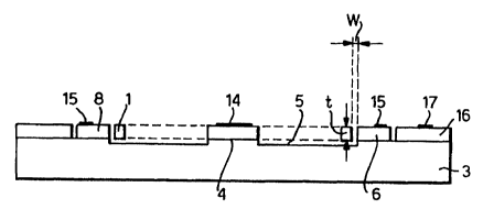
Figure 3 is a schematic cross sectional view taken on the line
A - A in Figure 2, and
Figure 4 is a cross sectional view similar to that of Figure 3 through a
sensor according to a second embodiment of the present invention.
An angular rate sensor according to the present invention suitable for
use as a vibrating structure gyroscope includes a substantially planar
vibrating
resonator 1 having a substantially ring or hoop-like shape structure with an
inner periphery 1 a and an outer periphery 1 b. The inner and outer
peripheries
1 a and 1 b extend around a common axis Z as shown in Figure 2 of the
accompanying drawings. The sensor also includes support means which in
turn include a plurality of flexible support beams 2 for supporting the
resonator
1 and for allowing the resonator 1 to vibrate, when driven, in a substantially
undamped oscillation mode such as to permit the resonator 1 to move relative
to the support means in response to turning rate. The support means also
includes a base 3 made from electrically insulating material and having a
projecting boss 4. The base 3 which is made from electrically insulating
material has means for electrically grounding it. The inner periphery 1 a of
the
resonator 1 is coupled to the boss 4 by the support beams 2 which extend from
the inner periphery 1 a to the boss 4 so that the ring or hoop-like shape
resonator structure is spaced from the boss 4 as can be seen in Figures 3 and
CA 02338616 2001-O1-24
WO 00/09971 PCT/GB99/02459
_g_
4. The total stiffness of the support beams 2 is less than that of the ring-
like
resonator 1. In this manner a cavity 5 is provided in the region directly
under
the ring-like resonator 1 and support beams 2 so that they are freely
suspended
from the boss 4. In the embodiments of the sensor of the present invention
illustrated in Figures 2, 3 and 4 of the accompanying drawings, there are 8
equi-angularly spaced support beams 2.
The beams have the effect of point spring masses acting on the
resonator at the point of attachment. As such they locally perturb the mode
dynamics causing a shift in the resonant frequencies. In order to prevent this
introducing an undesirable splitting of the carrier and response mode
frequencies the number and position of the legs should be matched to the
mode symmetry. When employing Cos 2A modes eight identical beams 2 at an
equi-angular separation of 45° are employed. The respective dimensions
of the
beams 2 and resonator 1 are such that the total stiffness of the beams 2 is
significantly less than that of the resonator 1 itself. This ensures that the
Cos26
behaviour is determined predominantly by the resonator characteristics of the
ring part of the resonator.
This has two distinct advantages. Firstly, the beam compliance serves to
decouple the ring resonator from the base mount giving significantly reduced
sensitivity to thermally induced mounting stresses. Secondly, any frequency
split present due to manufacturing imperfections may be trimmed out using the
mechanical balancing process described in GB 2292609A. This technique
involves the removal of mass from the neutral axis of the ring-like resonator
1
CA 02338616 2001-O1-24
WO 00/09971 PC'T/GB99/02459
-10-
and allows for accurate balancing of the carrier and response mode
frequencies. This balance will be maintained over the full operating
temperature range. This process can only be successfully applied where the
resonance behaviour is dominated by the ring-like resonator characteristics.
The resonant frequencies of ring structures such as described in US 5450751
will be substantially unaffected by this process as the resonance
characteristics
are predominantly determined by the support leg dimensions.
The resonator structure is excited into resonance at the Cos28 mode
frequency by means of electostatic drive means with the resultant motion
detected using electrostatic pick-off means.
The support beams 2 and resonator 1 are made from crystalline silicon
and the sensor also includes electrostatic drive means for causing the
resonator 1 to vibrate and electrostatic sensing means for sensing movement of
the resonator 1. The electrostatic drive means and electrostatic sensing means
include plate-like elements 6, 7, 8 and 9 made from crystalline silicon in the
form of transducers having surfaces 10 located substantially normal to the
plane of the resonator 1 at a spacing 11 from the adjacent outer periphery 1 b
of
the resonator 1.
The electrostatic drive means includes two electrostatic carrier mode
plate-like drive elements 6 for causing the resonator 1 to vibrate in a Cos29
carrier mode, which carrier mode drive elements 6 are located at 0° and
180°
with respect to a fixed reference axis R located in the plane of the resonator
1.
The reference axis R is taken from the geometric centre of the resonator 1 to
CA 02338616 2001-O1-24
WO 00/09971 PCT/GB99/02459
_ -11 -
the centre point of the one of the carrier mode drive elements 6. The
electrostatic drive means also includes two electrostatic response mode plate-
like drive elements 8 located at 45° and 225° with respect to
the reference axis
R.
The electrostatic sensing means includes two electrostatic carrier mode
plate-like pick-off elements 7 located at 90° and 270° with
respect to the
reference axis R and two response mode plate-like pick-off elements 9 for
sensing motion of the resonator 1 in response to rotation of the sensor about
an
axis normal to the plane of the resonator 1, namely the axis Z, which response
mode pick-off elements 9 are located at 135° and 315° with
respect to the
reference axis R.
When the sensor is rotated about the Z axis, Coriolis forces will couple
energy into the response mode with an amplitude of motion directly
proportional
to the applied rate. This motion is detected by the pick-off elements 9. The
rate induced motion may be nuiled by means of the response mode drive
elements 8 to enable the sensor to be operated in a closed loop configuration
which is known to give performance advantages. In this mode of operation the
nulling force is directly proportional to the applied rate.
As aforesaid the drive and pick-off transducers are identical plate-like
elements formed from the crystalline silicon. The plate surface 10 normal to
the
plane of the resonator 1 forms a capacitor with the facing surface of the
adjacent segment of the resonator 1. The plate subtends an angle of 40°
with
a 5° angular spacing between adjacent transducer elements. The
capacitor
CA 02338616 2001-O1-24
_ WO 00/09971 PCT/GB99/02459
-12-
spacing 11 is maintained at a constant value across the area of the capacitor
plates. The transducer sites and central boss 4 of the resonator 1 are rigidly
fixed to the supporting base 3 which comprises an electrically insulating
material such as glass. A silicon substrate with an insulating surface oxide
layer 13 may alternatively be used as shown in Figure 4.
The resonator structure is maintained at a fixed DC bias voltage with
respect to the drive and pick-off elements. The electrical connection from the
control circuitry is made, by means of a bond wire (not shown), onto a metal
bond pad 14 deposited onto the surface of the resonator structure at the
central
boss 4. Bond pads 15 are similarly deposited on the upper surface of the drive
and pick-off elements.
The ratio of the thickness (t) of the resonator 1 at the outer periphery 1 b
thereof to the width {w) of the spacing 11 between the resonator periphery 1 b
and the adjacent plate-like drive or pick-off element surfaces 10 according to
the invention must be in the range of from 10:1 to 40:1 to maximise the
capacitance between the resonator 1 and elements 6, 7, 8 and 9 and thereby
optimise the drive force on the resonator 1 for a given applied voltage and
also
to optimise the sensitivity of the electrostatic sensing means provided by the
elements 7 and 9.
An oscillating voltage, applied to a drive element 6 will generate a drive
force, F given by:
F = e° /~' ~/p~ VP . . . ( 1
d
CA 02338616 2001-O1-24
WO 00/09971 PCT/GB99/02459
-13
where V~ is the fixed DC offset voltage, Vp is the oscillating voltage applied
to
the drive element 6 at the resonant frequency w, d is the capacitor plate
separation, A is the capacitor plate area and eo is the permittivity of free
space.
The resonance motion modulates the pick-off element spacing 11 and hence
the capacitance. This will generate a current at the pick-off element 7, IPO.
which is given by:
s A
- 2 V aw
PO d DC . . . (2)
where a is the amplitude of motion which is assumed to be small in comparison
to the capacitor spacing d. The closed loop scalefactor when using capacitive
drive and pick-off transducers is given by:-
S F = m ~d2 I Uref
18 0 C 2 V 2 . . . (3)
DC
where m is the modal mass of the resonator 1, C9 is the transducer
capacitance and V~ef is the fixed voltage reference level of the primary pick-
off
output (this maintains a constant carrier mode amplitude). As the resonator 1
CA 02338616 2001-O1-24
WO 00/09971 PCT/GB99/02459
-14
and elements 6,7,8,9 are all fabricated from the same bulk Silicon wafer the
geometry of the overall structure will be very stable as the temperature
varies.
The voltage levels can also be maintained to a high degree of accuracy and
thus the scalefactor will be substantially constant over temperature. This
represents a significant improvement over the corresponding situation when
employing inductive drives and pick-offs which exhibit a B2 dependence.
Direct capacitive coupling of the drive signal onto the pick-off can. An
electrically grounded screen 16 is provided which encloses the drive and pick-
off elements on all surfaces normal to the plane of the resonator except the
surface 10 facing the outer periphery 1 b of the resonator 1. This screen 16
is
formed from the same Silicon wafer layer as the resonator 1 and transducer
plates allowing the drive and pick-off elements to be in close proximity to
one
another without giving rise to undue pick-up levels. The elements are then
able
to subtend a larger angle which helps to maximise the drive and pick-off
element gains.
Parasitic capacitive coupling between the drive and pick-off elements
may also occur indirectly where the DC bias offset of the resonator 1 is
inadvertently modulated by the applied drive voltage. The magnitude of this
modulation is determined by the ratio of the effective drive transducer gap
resistance, R9aP, to that of the bias offset bond pad to ring circumference
resistance (n.b. this is dominated by the support beam resistance, R,e9). This
error source may be contained within acceptable limits by selecting silicon
wafer material of resistivity such that Rgap » Rie9. Alternatively, by
depositing
CA 02338616 2001-O1-24
WO 00/09971 PCT/GB99/02459
-15
metal over the upper surface of the resonator 1 and support beams 2 then
silicon of considerably higher resistivity may be used.
The resistivity of the crystalline silicon is such that the effective drive
transducer gap resistance, that is the effective drive means spacing
resistance,
is substantially greater than the support beam resistance.
Where the substrate or base 12 consists of a silicon wafer with an
insulating oxide surface layer 13 such as in Figure 4, an additional parasitic
coupling mechanism exists. In order to eliminate capacitive coupling via the
silicon under the oxide surface layer, the substrate 12 must additionally be
electrically connected to ground. This may be conveniently done in the control
circuitry with electrical connection being made directly to the substrate. If
the
sensor is contained in a grounded metal package this may be conveniently
done by means of conductive epoxy applied between the underside of the
sensor and the surface of the package. Alternatively, this may be achieved on
the device chip by etching an additional hole in the silicon screen layer,
through
the surface oxide, to expose the substrate surface as shown in Figure 4. A
metal bond pad 18 may then be deposited directly onto the silicon substrate
and a wire bond connection 19 made to the screen layer from a bond pade 20.
In order to optimise the achievable drive force for given applied voltages
it is desirable to maximise the capacitor plate area and minimise the spacing
11
size (i.e. maximise capacitance). The capacitor area may be increased by
increasing the radius and the depth or thickness (t) of the resonator 1. The
requirement to maintain the natural mode frequencies above any input vibration
CA 02338616 2001-O1-24
WO 00/09971 PCT/GB99/02459
-16
range imposes some limitations on these dimensions. For resonator structures,
such as described herein, where the resonator 1 is significantly stiffer than
the
support beams, the lowest frequency resonance will be an out of plane
translation of the resonator 1. Increasing the radius of the resonator will
lower
this mode frequency, however, this may be partially offset by increasing the
depth of the structure. Modern Deep Reactive Ion Etch (DRIE) equipment and
techniques are capable of etching high quality vertical trenches in silicon to
a
depth of several hundred microns. This provides the capability of fabricating
capacitors with large plate areas. However, maximising the capacitance is also
dependent upon reducing the spacing 11.
The sensor dimensions are designed to give the optimum solution to
accommodate all of these design requirements. The structure shown in Figure
2 has a resonator radius of 2mm with a rim width of 50~m. The support beams
2 are 24~,m wide with the total stiffness of all support beams being
significantly
less than that of the resonator 1. The capacitor spacings 11 are 10~.m and
thus, with a resonator ring depth or thickness (t) of 100~m the aspect ratio
of
the trench is 10:1. The use of a capacitor spacing of this dimension enables
adequate transducer gain to be achieved with low offset voltages on the
resonator (~5V). This avoids the need to generate voltages in excess of the
supply and facilitates low cost ASIC integration. Using these dimensions a
sensor with performance and manufacturing cost commensurate with current
high volume automotive requirements can be fabricated.