Note: Descriptions are shown in the official language in which they were submitted.
CA 02338661 2001-O1-26
a
r
Translation of WO 00/07151 (PCT/EP99/05390)
Safety Paper, Method and Device for Checking the Authenticity of
Documents Recorded Thereon
The invention relates to a safety paper having a structure
making possible a contactless checking of an authenticity feature
and to a method for checking the authenticity of documents which
are recorded in an optically readable form on the safety paper.
The use of such safety papers for producing documents serves
for protecting them against unauthorized reproduction by forgers.
This is necessary, in particular, for securities such as bank
notes, checks, travelers checks, stocks, etc. There is also a need
for securing papers which do not have a direct monetary value, such
as identification papers, passports etc., against unauthorized
copying. The employed term "document" is therefore meant to
include all types of securities and identification papers to be
protected against unauthorized copying.
In particular, in the case of securities which are circulated
daily, for example, bank notes, a forger may succeed in copying the
optically recorded document contents, for example, the optical
printed image of the bank notes, in a deceptively precise way. A
protection against this is the authenticity feature contained in
the safety paper, used for producing the documents, as a result of
the structure imparted to the safety paper during manufacture which
authenticity feature supposedly practically cannot be copied by a
1
__._. ...... ~ 02338661 2001-O1-26 ..__.____..._......
r
forger with the means available to him. Moreover, the application
of watermarks or the introduction of a safety thread into the paper
is known. In particular, it is known (DE 29 05 441 C3) to
introduce into the paper layer a magnetizable or electrically
conducting safety strip. These conventional measures, however, can
no longer be considered satisfactory. In particular, in
the case of global political crisis regions the war-conducting
groups or even entire countries employ forgery as warfare.
Accordingly, the resources employed for forgery are correspondingly
great.
In a bank note produced from a known safety paper (DE 196 30
648 A1), a transponder chip with an antenna is integrated into the
bank note in a way similar to that of safety strips of different
kinds integrated into conventional bank notes. The pattern which
serves as the antenna has the shape of an antenna coil which is
formed as a thick or thin layer structure directly on the
transponder chip. As an alternative, the transponder chip can be
localized in the neighborhood of the metal safety strip or at an
interrupted portion of the metal safety strip and can be surrounded
by the antenna coil. According to a further possibility, the metal
safety strip is modified such that it forms itself the antenna coil
for the transponder chip. The attachment of the antenna coil on
the transponder chip itself results in a very small coil cross-
section with correspondingly small sending and receiving
sensitivity. Moreover, it is difficult with regard to
manufacturing technology to anchor the small transponder chip on
the bank note. The other aforementioned options, in which the
antenna coil is arranged outside of the transponder chip on the
bank note, provide the possibility of forming greater coil cross-
sections but the formation and connection of the antenna coil to
the transponder chip on the bank note is problematic with regard to
manufacturing technology.
2
AMENDED SHEET
CA 02338661 2001-O1-26
In another known safety paper (DE 196 Ol 358 A1) which is
suitable, in particular, for bank notes, a transponder chip which
may comprise a read-only storage and/or a write/read storage, is
embedded in the paper layer and contains in the simplest case an
imprinted identification number which can be read contactless and
which serves as an authenticity feature. With respect to the data
transmission it is disclosed generally that it can be carried out
by a modulation of an alternating current in an inductive or
capacitive way. For the inductive transmission a miniaturized coil
is provided on the transponder chip. For the transmission across
greater distances, it is noted generally that in a manner known in
the art an antennas, coils with larger enveloping surface area, or
dipoles are arranged on the chip.
Finally, it is also known to use a photoehrome imprint as a
safety feature for documents which, in a reversible way, can change
its color (GB 2 272 861 A).
It is an object of the invention to provide a safety paper of
the aforementioned kind with improved forgery-proof properties and
verification as well as a method and a device for automatic
checking of the authenticity of the documents produced on the
safety paper.
2a
AMENDED SHEET
""""-~~CA 02338661 2001-O1-26
According to the invention, this object is solved by the
combinations of features as defined in the claims.
According to the inventive embodiment of the safety paper, the
checking with regard to the presence of the authenticity feature is
carried out in that an input signal, which triggers emitting an
output signal, is transmitted to the circuit extending within the
paper plane. Preferably, the input signal as well as the output
signal are in the form of.a carrier frequency oscillation modulated
with the corresponding signal information, respectively. With a
corresponding configuration of the circuit any desired information
contents, preferably in binary form, can be encoded in the output
signal as an authenticity feature. It is possible to provide the
electronic circuit with a micro controller. By doing so, it is
possible to assign at least one individual authenticity feature,
for example, the individual serial number of the micro controller,
to any document produced on the safety paper. For example, in the
case of a bank note, this can reside in that the authenticity
feature represents in encoded form the monetary value and/or the
serial number of the bank note provided on the optically readable
printed image of the bank note. In a method for checking
authenticity according to claim 15, the optically readable contents
of the document, in the exemplary embodiment the monetary value of
the bank note and/or its serial number, and the output signal of
the circuit encoding the contents can be automatically detected and
compared with one another. The authenticity of the document, for
example, the bank note, is confirmed by this method only when
between the optically read contents and the information contents of
the output signal of the circuit a predetermined correlation, for
example, content identity, is present.
3
AMENDED SHEET
CA 02338661 2001-O1-26
A method according to claim 18 and a document according to
claim 21 particularly take into account that especially bank notes
can be separated into two parts and the respectively missing part
can be replaced by forgery. By providing a generally invisible
authenticity feature, which can however be detected by technical
means, for example, magnetically or by light not within the visible
range, in one part and by storing information corresponding to this
authenticity feature in the circuit on the other part, the two
parts are coupled to one another in a forgery-proof way. The
information contents corresponding to the detected authenticity
feature is entered into the circuit during the authenticity check
and is checked therein with regard to authenticity, for example, by
comparison to reference information. The circuit only provides the
output signal acknowledging authenticity when this authenticity
check is positive.
An expedient embodiment of the inventive concept is that the
structure forming the circuit comprises a read-only storage having
a predetermined information contents, wherein the information
contents can be transmitted with the emitted output signal. In
this connection, the information contents corresponding to the
authenticity feature is permanently pre-set in the read-only
storage and is transmitted with the emitted output signal.
In the context of the invention it is also provided that the
structure forming the circuit comprises a write/read storage into
which the information contents transmitted by the received input
signal can be written, wherein the transmitted information contents
can be transmitted with the emitted output signal.
In this embodiment, the input signal not only serves to access
the fixedly adjusted authenticity feature which is permanently
correlated with the document produced on the safety paper;
AMENDED SHEET
CA 02338661 2001-O1-26
moreover, the information contents can be transmitted to the
circuit with the input signal and can be stored therein and, in
response to a subsequently received receiving signal, can also be
transmitted with the emitted output signal. This embodiment is
especially important with respect to the method claimed in the
claims 16 and 17. In this connection, at each location which
examines the document produced on the safety paper, for example, at
each bank which receives a bank note during its circulation, the
examining location and optionally also the date of the examination,
representing the information contents, is written into the circuit
with the input signal during the checking process, for example,
during a money counting process. During the subsequent checking
processes, this information contents is transferable by means of
the emitted output signal and provides in this way a local and
temporal proof of stations which have been passed. Unauthorized
money-laundering activities can thus be precisely traced.
With respect to circuit-technological considerations, this is
realized especially simply in that the write/read storage is formed
by a shift register into which the binary representation of the
information contents transmitted by the input signal can be
sequentially stored. In this connection, the length of the shift
register, as a function of the magnitude of the information
contents transmitted by the individual examination locations,
determines the total number of storable checking activities. Since
the information contents are pushed through from the input of the
shift register to its output, the latter always contains the most
recent state of these information contents while the information
contents of examinations that are not so recent and surpass the
storage capacity of the shift register are moved out of the shift
register.
AMENDED SHEET
CA 02338661 2001-O1-26
Another important principle of the invention resides in that
the structure forming the circuit comprises an energy supply which
can be recharged by contactless energy transmission. In this
respect, it is especially expedient that the energy transmission is
realized by a carrier frequency oscillation provided for modulation
with the input signal. By doing so, the energy supply of the
circuit can be realized completely from the exterior by the method
described in claim 21, and the circuit does not require its own
operating energy source; as a result of its limited service life
and the fact that, in any case, it can hardly be formed paper- thin
with current means, providing such energy source would present
6
AMENDED SHEET
..... ~ 02338661 2001-O1-26 -_...."..........,..__.. . .
great difficulties with regard to a practical and economical
realization of the safety paper.
Different possibilities are conceivable in regard to how to
manufacture the circuit in or on the safety paper. One of these
possibilities provides that the structure forming the circuit is
embedded in the paper layer of the safety paper. In this case, the
circuit is covered on both sides by partial layers of the paper
layer. In contrast, another very expedient alternative is that the
pattern which forms the sending/receiving antenna is applied
externally to the paper layer and is coupled by the paper layer,
which serves as a dielectric, in a capacitive way to the remaining
portion of the circuit embedded in the paper layer. This
alternative can be produced, for example, in that the remaining
part of the circuit is pre-manufactured on a thin flexible
substrate and is introduced into the paper layer during the paper
manufacture while the antenna_pattern is applied, for example, by
printing, onto the paper layer provided with the embedded part of
the circuit. Between the connecting portions of the pattern,
serving as a sending/receiving antenna, arranged on the paper layer
and the areas of the embedded flexible substrate serving as
connecting portions for the remaining part of the circuit, a part
of the paper layer acting as the dielectric is therefore provided,
respectively, which, together with the connecting portions,
positioned above one another on both sides of this part of the
paper layer, of the antenna pattern and of the embedded flexible
substrate, forms a capacitor effecting a capacitive coupling.
In a preferred embodiment of the safety paper it is provided
that the structure forming the circuit comprises an electronic
7
CA 02338661 2001-O1-26
circuit chip and a pattern connected therewith and serving as a
sending/receiving antenna. The conductor pattern forming the
sending/receiving antenna allows an effective signal transmission,
in particular, when realized by a modulated carrier frequency to
which the antenna pattern is tuned. Since the surface area of the
circuit is very small in comparison to the format surface of the
bank notes and other documents, plenty of space is available for
the antenna pattern.
An especially expedient embodiment is realized in that the
structure forming the circuit comprises an integrated polymer
circuit chip which is formed on a flexible polymer substrate. This
embodiment takes advantage of the known modern polymer circuit
techniques (compare IEDM 97-331 "Polymeric Integrated Circuits and
Light-Emitting Diodes" or The American Association for the
Advancement of Science, vol. 278, No. 5337, 17 October 1997, pp.
383-384 "Patterning Electronics on the Cheap").
Preferably, the pattern serving as the sending/receiving
antenna has the shape of a dipole antenna.
Because of its simple straight form, the dipole antenna makes
possible a simple manufacture of the safety paper. In particular,
it can be realized as a straight linear strip across a large paper
web, wherein the individual dipole antennas of the documents to be
produced from the paper web by cutting are produced automatically
by the cutting process. The sending/receiving directional
characteristic connected with the dipole antenna is also
advantageous. For example, bank notes which are stacked are
conventionally counted in counting machines such that the
8
_~ 02338661 2001-O1-26 ____. __.
respectively uppermost, bank note of the stack is turned about one
of its longer lateral edges and is then placed onto a new stack.
Inasmuch as the dipole antenna extends perpendicularly to this
lateral edge, it passes during this turning process through a plane
which extends perpendicularly to the stack plane so that, for a
suitable alignment of the sending/receiving characteristic of the
counting machine, the coupling for the bank note, aligned during
the turning movement perpendicularly to the stack plane, is at a
maximum and a feedover of the other bank notes of the stack is
suppressed. It is understood that the modulated carrier frequency
used for the signal transmission is adjusted to the size of the
dipole antenna.
Various possibilities are conceivable in regard to how to
realize the circuit chip and its dipole antenna on the safety
paper. Preferably, it is suggested that the pattern which forms
the dipole antenna is comprised of two conductor strips extending
along a common straight line which are contacted via their
oppositely positioned ends with connecting areas of the circuit
chip. In this connection, it is particularly expedient that the
two conductor strips are formed by portions of an insulating thin
polymer substrate strip that have been made conducting between
whose insulating portion, delimited by the ends of the conductor
strips facing one another, the circuit chip is arranged. The
conducting portions of the insulating thin polymer substrate strips
can be generated, for example, by doping. It is also very expedient
to metallize, i.e., to provide with a thin metal layer, a larger
polymer web with the exception of the insulating portions serving
for receiving the circuit chips and to produce the polymer
substrate strips therefrom by cutting. In the case of producing
9
CA 02338661 2001-O1-26
the conductivity by metallization of one side of the polymer
substrate strip, the other side can be provided, as an additional
measure, with a photovoltaic layer which can serve as an exclusive
or additional supplier of operational energy for the circuit.
Furthermore, it is expedient to provide the conductor strip with
cutouts, in particular, fine perforations, so that the clamping
action with the paper layer is improved.
The connection with the circuit chip can be realized in that
the circuit chip is formed on a thin-ground semiconductor substrate
which is arranged on the insulating portion of the polymer
substrate strip. Techniques for thin grinding of the semiconductor
substrate are known.
As an alternative, it can be provided that the circuit chip is
an integrated polymer circuit chip formed on a flexible polymer
substrate provided with a pattern forming the dipole antenna. This
embodiment takes advantage of the known modern polymer circuit
techniques (compare IEDM 97-331 "Polymeric Integrated Circuits and
Light-Emitting Diodes" or The American Association for the
Advancement of Science, vol. 278, No. 5337, 17 October 1997, pp.
383-384 "Patterning Electronics on the Cheap").
An embodiment which is advantageous in all situations resides
in that the circuit chip and the pattern forming the dipole antenna
are embedded in the paper layer of the safety paper. In this case
the circuit chip and the dipole antenna are covered on both sides
by partial layers of the paper layer.
CA 02338661 2001-O1-26
Another basic principle of the invention resides in that the
structure comprises an electro-optical surface area containing the
authenticity feature whose light reflection or transmission
properties can be controlled as a function of an electrical
potential supplied to the surface area. In this case, the
authenticity feature can be formed in the surface area, for
example, in the form of a document number or bank note number or
other identification symbols in positive form or negative form.
During the authenticity check the control potential is
supplied to this surface area. The thus caused change of the light
reflection or transmission then allows optical recognition of the
authenticity feature.
As in the afore described embodiments, the required potential
for controlling the electro-optical surface area can be generated
by contactless introduction of HF energy. An especially
advantageous alternative in regard to electrical energy supply,
however, resides in that the structure comprises a photovoltaic
surface area which serves as an energy supplier. In this case,
during the safety check it is only required to supply light onto
the photovoltaic surface area of the safety paper. The
photovoltaic surface area provides in response to the input light
the electrical operating energy for the safety structure. This
particularly advantageous kind of energy supply is not limited to
safety paper and documents produced therefrom. It is also suitable,
in particular, for the contactless energy supply of intelligent
hard plastic cards, as known, for example, in the form of smart
cards and similar plastic cards with integrated electronic
components used, in particular, for payments.
11
AMENDED SHEET
CA 02338661 2001-O1-26
Such electro-optically controlled surface areas can be
produced, in particular, by sputtering methods with which, in
vacuum or in special gas atmospheres, metals or metal alloys can be
applied in thin layers on thin plastic films. The thus coated
plastic films, whose coating has been generated during the coating
process, or also subsequently thereto, as a pattern that represents
the authenticity feature in a positive or negative form, can then
be applied onto the safety paper or embedded in its paper layer.
The invention also provides a device for contactless checking
of authenticity of a document made of a safety paper which is
provided with an electronic circuit chip as well as with a pattern
connected therewith and being in the form of a dipole antenna
having two dipole branches extending along a common straight line
and serving as a sending/receiving antenna, wherein the electronic
circuit chip in response to a received input signal emits an output
signal representing the authenticity feature, wherein the device
has a transport device by which the document to be checked can be
transported along a movement path extending transverse to the
common straight line of the dipole branches, two conductors
extending in the transport direction, one arranged in the area of
the movement path of one dipole branch and the other in the area of
the movement path of the other dipole branch for a capacitive
coupling with the moving dipole branches, respectively, and a
sending/receiving device coupled with the two conductors for
emitting the input signal for the circuit chip and for receiving
its output signal representing the authenticity signal.
12
AMENDED SHEET
CA 02338661 2001-O1-26
In this checking device embodied according to the invention,
the two conductors serving as the antenna for the sending/receiving
device of the checking device extend over a sufficient length of
the movement path of the document to be checked so that over this
entire path length a uniformly strong coupling to the dipole
antenna of the respective document to be checked is ensured. The
dipole antenna of the document to be checked can have a relatively
minimal extension in the transport direction while the two
conductors of the checking device are comparatively long in
comparison thereto.
In the following description the invention is explained in an
exemplary fashion with reference to the drawing. It is shown in:
Fig. 1 a plan view onto the front side of a travelers
check on which the realization of an electronic
circuit which serves for authenticity checking is
schematically indicated;
Fig. 2 a view onto the backside of the travelers check
illustrated in Fig. 1;
13
AMENDED SHEET
CA 02338661 2001-O1-26
Fig. 3 a view corresponding to Fig. 1 of another
embodiment;
Fig. 4 a plan view onto the backside of the embodiment of
Fig. 3;
Fig: 5 a schematic illustration of a checking device; and
Fig. 6 an embodiment variant of Fig. 1 in a plan view.
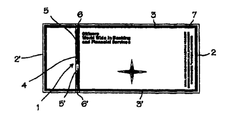
The travelers check of an internationally known bank
illustrated in the drawing is supplemented for the purpose of
explaining the invention by the schematic illustration of an
electronic circuit. The latter has a polymer strip 1 which is made
conductive by doping and is embedded in the paper layer. This can
be realized in a manner known in the art in that during the paper
manufacture first the first partial layer of the paper pulp is
deposited, the polymer strip 1 is placed thereon, and,
subsequently, a second partial layer of the paper pulp is applied.
The polymer strip 1 extends parallel to the two shorter lateral
edges 2, 2' over the entire width of the rectangular travelers
check up to its longer lateral edges 3, 3'. Even though the
polymer strip 1 is covered on both sides by the paper layer, it is
illustrated in the drawing so as to show through the layers
covering it.
In the center of the polymer strip 1 an integrated polymer
circuit chip is formed whose external terminals are formed by the
two partial strips 5, 5' of the polymer strip 1 extending on both
sides of the polymer circuit chip 4. The two partial strips 5, 5'
14
CA 02338661 2001-O1-26
are coupled at their ends 6, 6' positioned on the longer lateral
edges 3, 3' capacitively or electrically with the antenna pattern
7 which extends, starting at the ends 6, 6', in the form of a
conductor along the two longer lateral edges 3, 3' and the shorter
lateral edge 2 connecting these two lateral edges.
The antenna pattern 7 could also be embedded during the paper
manufacture in the paper layer in that it is generated, for
example, by printing it onto the first deposited partial layer of
the paper pulp. However, the antenna pattern 7 is printed in a
simpler way and without safety loss externally onto the paper layer
provided with the embedded polymer strip 1. In this case, the ends
of the antenna pattern 7 positioned above the polymer strip 1
overlap the ends 6, 6' of the two partial strips 5, 5' positioned
on the longer lateral edges 3, 3' within the paper layer, wherein
between the overlapping areas of the antenna pattern 7 and the
polymer strip 1 a partial layer of the paper layer is enclosed,
respectively. This partial layer thus acts as a dielectric by
which the antenna pattern 7 is coupled capacitively with the
polymer strip 1 provided with the polymer circuit chip 4.
The polymer circuit chip 4 forms a micro controller with a
read-only storage, a shift register serving as a write/read
storage, and an input/output unit which comprises a receiving
portion and a sending portion. The number as well as the monetary
value of the travelers check printed on the front side of the
travelers check as optically readable plain text are stored in the
read-only storage.
CA 02338661 2001-O1-26
The checking of the authenticity requires the travelers check
to be guided through a checking device which reads, on the one
hand, the printed, optically readable data such as check number and
monetary value. At the same time, this reading device emits a
carrier-frequency based, modulated input signal for the circuit 1,
4, 7. This input signal is decoded in the receiving portion of the
circuit. In response to this, the micro controller controls the
read-only storage and the sending portion for a carrier frequency
modulated emission of an output signal in which the information
contents of the read-only storage is encoded. The checking device
detects this output signal and compares the information contents
transmitted therewith with the optically detected plain text data
of the travelers check. If no match is detected, the travelers
check is identified as forged.
An even higher safety is achieved when the document, for
example, the bank note or travelers check, is provided additionally
with an authenticity feature, which is not optically readable but
readable by other technical means, for example, by UV light or
magnetically, at a location which differs from the location of the
circuit. In this case, the checking device detects this
authenticity feature and transmits the information corresponding to
the detected authenticity feature to the circuit. Here, the
authenticity feature is checked internally, for example, by
comparison with a reference information stored in the circuit. The
circuit emits an output signal indicating authenticity to the
checking device only in the case of a positive checking result.
The checking location transmits with the input signal an
information contents identifying it, for example, the name and
16
CA 02338661 2001-O1-26
place of the bank receiving the travelers check in addition to the
date of the checking operation. At the same time, the receiving
bank can transmit and store with the input signal identifying
information of the person submitting the travelers check, for
example, the name and address. This information identifying the
person submitting the check is of interest, in particular, when a
location which has received the travelers check originally from the
issuing person, transfers this travelers check to a third person as
legal tender and this third person appears at the bank as the
person redeeming the check. This identification information is
entered by the micro controller in binary form serially into the
shift register wherein, if needed, a portion of previously entered
information overflows at the output of the shift register and is
lost.
The input signal transmitted from the checking device to the
circuit can also be encoded with a command for reading the contents
of the shift register with simultaneous re-writing of the read
information contents. By transmitting the entire contents of the
shift register in the output signal of the circuit, the checking
device can detect and process this information contents. In this
way, it is possible to determine with the checking device through
which checking locations the document to be checked has already
passed previously and at what point in time. This is particularly
important when the documents are bank notes provided with the
circuit 1, 4, 7 which, during the course of their circulation, are
counted again and again by the receiving banks. In this way, the
circulation path of these bank notes can be monitored.
17
CA 02338661 2001-O1-26
In the case of travelers checks their safety can be further
enhanced in that the drawee bank, when issuing the travelers check,
can store an identification code, for example, a pin code, that the
check owner has agreed to, in the read/write storage. Inasmuch as
the receiving location accepting the travelers check is provided
with a suitable device for reading this additional identification
code, it can request, for authenticity checking, this additional
identification code to be disclosed by the issuer of the check in
order to compare it with the read version of the additional
identification code. Should no match be present, the travelers
check is to be disposed of as forged.
An energy supply, which is integrated in the polymer circuit
chip 4 and supplies the operating energy for the circuit 1, 4, 7
provided on the travelers check, is supplied by the carrier
frequency oscillation of the input signal transmitted by the
checking device. In this way, the checking device transmits the
required energy for the operation of the circuit.
It is understood that the employed safety paper for the
manufacture of the afore described travelers check is produced in
the form of webs which, according to the format, have the polymer
strips 1 embedded therein as continuous strips and are provided
with the corresponding antenna pattern. This paper web is
subsequently printed on both sides and is then cut to size
according to the desired format so that the individual pieces of
travelers checks or the like are generated.
In the embodiment illustrated in Figs. 3 and 4, the travelers
check has an electronic circuit which is formed by a thin chip 40.
18
CA 02338661 2001-O1-26
The chip 40 is arranged on a polymer strip 10 which is embedded in
the paper layer. This can be carried out as is known in the art in
that during the paper manufacture first a first partial layer of
the paper pulp is deposited, the polymer strip 10 is placed
thereon, and subsequently a second partial layer of the paper pulp
is applied. The polymer strip 10 extends parallel to the two
shorter lateral edges 20, 20' over the entire width of the
rectangular travelers check up to its longer lateral edges 30, 30' .
Even though the polymer strip 10 is covered on both sides by the
paper layer, it is illustrated in the drawing so as to show through
the layers covering it.
The polymer strip 10 is, for example, made conductive by
doping or by an applied metallization. Only in the center between
the two lateral edges 30, 30' where the integrated circuit chip 40
is arranged, the conductive doping or metallization layer is
interrupted such that connecting areas of the chip 40 formed on
oppositely positioned edges 70, 70' of the chip 40 are contacted by
one of the two partial strips 50, 50' of the polymer strip 10
extending on both sides of the interrupted portion, respectively.
The two partial strips 50, 50' form in this way a dipole antenna
connected to the chip 40 which serves for signal transmission as
well as transmission of operating energy for the chip 40.
Like the polymer circuit chip 4 of the embodiment of Figs. 1
and 2, the circuit chip 40 of the embodiment of Figs. 3 and 4 also
forms a micro controller with a read-only storage, a shift
register serving as a write/read storage, and an input/output unit
comprising a receiving portion and a sending portion. In the read-
only storage the number as well as the monetary value of the
19
CA 02338661 2001-O1-26
travelers checks printed on the front side of the travelers check
in optically readable plain text are permanently stored. The
checking for authenticity is carried out in the same way as
explained above for the embodiment of Figs. 1 and 2.
Bank notes have the same appearance as the travelers check
explained in connection with Figs. 1 and 2. The counting of such
bank notes is carried out usually in that from a stack of bank
notes to be counted the uppermost bank note, respectively, is
turned about one of its longer lateral edges 30 or 30' and is in
this way transferred onto a counted stack. During this turning
process the conductor strips 50, 50' forming the dipole antenna
pass through a plane which is perpendicular to the longer lateral
edges 30, 30' so that the conductor strips 50, 50' at the center of
this turning movement are positioned perpendicularly to the plane
of the bank notes which are positioned on the stack to be counted
or on the stack already counted. By using the directional
characteristic of the dipole antenna, the checking device can be
arranged such that the maximal coupling to the dipole antenna 50,
50' is achieved in the center of the turning path of each bank note
between the stack to be counted and the counted stack.
Accordingly, feedover of the bank notes positioned on both stacks
can be suppressed during the counting process.
As with the embodiment of Figs. 1 and 2, an energy supply
integrated in the circuit chip 40 and providing the operational
energy is supplied by the carrier frequency oscillation of the
input signal which is transmitted by the checking device. As an
alternative or in addition, the operating energy could be derived
from a photovoltaic area arranged on the document. In this way,
CA 02338661 2001-O1-26
the checking device transmits the required energy for the operation
of the circuit chip 40.
The safety paper is produced in the form of webs in which,
according to the format of the bank notes, travelers checks,
documents etc. to be produced from the safety paper, the polymer
strip 10, with the chips 40 arranged thereat at a spacing
corresponding to the spacing of the lateral edges 30, 30', is
embedded so as to extend continuously. This paper web is
subsequently printed on both sides and then cut to size according
to the desired format so that the individual pieces of bank notes,
travelers check or the like are generated in which the partial
strips serving as a dipole antenna extend with their ends 60, 60'
to the lateral edges 30, 30' of the cut pieces.
Fig. 5, in which the essential parts of a checking device are
schematically illustrated, shows a document 100 to be checked, for
example, a bank note, which is transported by a transport device,
not represented, in a transport direction illustrated by arrow 101
along a movement path. The document 100 corresponds to the
embodiment illustrated in Figs. 3 and 4. The alignment of the
document .100 is such that the two conductor strips 50, 50'
connected to the circuit chip 40 and forming the dipole antenna
extend transverse to the transport direction 101.
The checking device has two elongate conductors 103, 103'
which extend with their longitudinal direction along the transport
direction 101 and are arranged such that one conductor 103 is
arranged in the area of the movement path of one dipole branch 50
and the other conductor 103' in the area of the movement path of
21
CA 02338661 2001-O1-26
the other dipole branch 50'. In this way, the document 100 during
movement through the checking device is coupled capacitively with
uniform strength to the two conductor paths 103, 103'. The latter
serve as a sending/receiving antenna for a sending/receiving device
104 of the checking device connected thereto. In this way, the
input signal for the circuit chip 40 is reliably transmitted from
the sending/receiving device 104 of the checking device and the
output signal emitted by the circuit chip 40 is reliably received.
The embodiment illustrated in Fig. 6 deviates from that of
Figs. 1 and 2 only with respect to the positional arrangement of
the circuit chip 4. Otherwise, there is complete identity with the
embodiment of Figs. 1 and 2, and, therefore, reference is being had
to the above description, wherein in Fig. 6 the same reference
numerals are used for the parts identical to those of Fig. 1.
Fig. 6 illustrates in deviation of Fig. 1 the asymmetric
position of the circuit chip 4 on the document relative to the two
transverse edges 2, 2' and the two longitudinal edges 3, 3'. In
this way, the circuit chip 4 avoids the area of the longitudinal
centerline extending in the center between the two longitudinal
edges 3, 3' and parallel thereto and also the area of the
transverse centerline of the document extending in the center
between the two transverse edges 2, 2' and parallel thereto.
Inasmuch as the document, in particular, a bank note, is folded
along the two imaginary center lines, the circuit chip 4 is not
affected by this folding action. This means that during
conventional folding no risk of damage is present. This asymmetric
positional arrangement of the circuit chip 4 is advantageous for
22
CA 02338661 2001-O1-26
all embodiments, in particular, also for the arrangement of the
circuit chip 40 of the embodiment illustrated in Figs. 3 and 4.
Often, documents, in particular, bank notes, have an area
which is not printed. In this area there is often a watermark in
the paper layer. In all embodiments it is advantageous to arrange
the circuit chip 4 or 40 in such areas without printed image so
that the loading of the circuit chips during the later printing
process is avoided.
In all embodiments it is also advantageous that the pattern
serving as the sending/receiving antenna is produced of a material
whose expansion coefficient substantially matches the expansion
coefficient of the paper layer connected to the pattern.
Distortions or warping of the safety paper or even detachment of
the pattern can thus be prevented.
23