Note: Descriptions are shown in the official language in which they were submitted.
CA 02338849 2001-01-25
WO 00/10143 PCT/US99/17901
CIRCUIT FOR ENERGIZING EAS MARKER DEACTIVATION
DEVICE WITH DC PULSES OF ALTERNATING POLARITY
FIELD OF THE INVENTION
This invention relates generally to electronic article surveillance (EAS), and
pertains
more particularly to so-called "deactivators" for rendering EAS markers
inactive.
BACKGROUND OF THE INVENTION
It has been customary in the electronic article surveillance industry to apply
EAS
markers to articles of merchandise. Detection equipment is positioned at store
exits to detect
attempts to remove active markers from the store premises, and to generate an
alarm in such
cases. When a customer presents an article for payment at a checkout counter,
a checkout
clerk either removes the marker from the article, or deactivates the marker bv
using a
deactivation device provided to deactivate the marker.
Known deactivation devices include one or more coils that are energizable to
generate
a magnetic field of sufficient amplitude to render the marker inactive. One
well known type
of marker (disclosed in U.S. Patent No. 4,510,489) is known as a
"magnetomechanical"
marker. Magnetomechanical markers include an active element and a bias
element. When
the bias element is magnetized in a certain manner, the resulting bias
magnetic field applied
to the active element causes the active element to be mechanically resonant at
a predetermined
frequencv upon exposure to an interrogation signal which alternates at the
predetermined
frequency. The detection equipment used with this type of marker generates the
interrogation
signal and then detects the resonance of the marker induced by the
interrogation signal.
According to one known technique for deactivating magnetomechanical markers,
the bias
element is degaussed by exposing the bias element to an alternating magnetic
field that has
an initial magnitude that is greater than the coercivity of the bias element,
and then decays to
zero. After the bias element is degaussed, the marker's resonant frequency is
substantially
shifted from the predetermined interrogation signal frequency, and the
marker's response to
the interrogation signal is at too low an amplitude for detection by the
detecting apparatus.
In one conventional deactivation device, a drive circuit occasionally applies
a drive
signal having a decaying AC waveform to a coil or coils. The drive circuit is
triggered to
generate the drive signal in response to a button or switch actuated by the
checkout clerk, or
by circuitry which detects the presence of an active marker.
CA 02338849 2008-04-16
77496-60
More recently, in co-pending patent applications
that are commonly assigned with the present application, it
has been proposed to eliminate the triggering mechanism and
to drive the deactivation device coil or coils with a
continuous wave AC sinusoid having constant amplitude (or a
periodically interrupted version of such a signal), as
disclosed in U.S. Patent No. 5,867,101, issued February 2,
1999; or with discrete single cycles of an AC sinusoid, also
with constant peak amplitudes, as disclosed in U.S. Patent
No. 6,111,507, issued August 29, 2000. In the case of both
of these coil excitation schemes, the required decay in the
signal actually applied to the EAS marker is accomplished by
sweeping the marker past the deactivation coils so that the
field applied to the marker is attenuated as the marker
exits the region in which the field is radiated.
Although sweeping markers past the deactivation
device coils can work quite effectively, it is sometimes
desirable to provide a deactivation device which does not
require the marker to be swept. An example of such a
deactivation device is the so-called "bulk" deactivator
disclosed in U.S. Patent No. 5,781,111. (The 1111 patent
has a common inventor and a common assignee with the present
application).
In addition, enhanced energy efficiency is another
desirable goal for marker deactivation devices.
OBJECTS AND SLJMMARY
It is a primary object of some embodiments of the
present invention to provide an efficient energizing circuit
for an EAS marker deactivation device.
2
CA 02338849 2008-04-16
77496-60
It is a further object of some embodiments of the
invention to provide an energizing circuit which makes the
deactivation device convenient to use.
According to an aspect of the invention, there is
provided an apparatus for deactivating a magnetomechanical
EAS marker, the apparatus including a coil for generating a
magnetic field to which the marker is to be exposed, the
coil having a first terminal and a second terminal, a
storage capacitor, a first switch connected between the
storage capacitor and the first terminal of the coil, a
second switch connected between the second terminal of the
coil and ground, a third switch connected between the
storage capacitor and the second terminal of the coil, a
fourth switch connected between the first terminal of the
coil and ground, and control means, comprising control
circuitry in one embodiment, for controlling the first,
second, third and fourth switches and causing the first and
second switches to be open and the third and fourth switches
closed during a first sequence of time intervals, and
causing the third and fourth switches to be open and the
first and second switches closed during a second sequence of
time intervals interleaved with the first sequence of time
intervals, and causing all of the first, second, third and
fourth switches to be open during a third sequence of time
intervals, a respective one of the third sequence of time
intervals intervening between each sequential pair of
intervals of the first and second sequences. The respective
durations of the intervals of the first and second sequences
are both monotonically decreasing over the course,
respectively, of the first and second sequences in one
embodiment. The control circuit preferably includes a
circuit for generating a ramp signal and a comparison
circuit for comparing a signal level at the coil with the
3
CA 02338849 2008-04-16
77496-60
ramp signal, and circuitry responsive to the comparison
circuit for selectively terminating the intervals of the
first and second sequences. At least one additional coil
may be connected in series or in parallel with the
aforementioned coil. The time intervals of the third
sequence, corresponding to "dead periods" between the
intervals of the first and second sequences in which the
coil is driven, are preferably much longer in duration than
the intervals of the first and second sequences, which are
quite short. Consequently, the effective duty cycle of the
deactivation device is very low, so that power consumption
is low.
According to another aspect of the invention,
there is provided a method of deactivating a
magnetomechanical EAS marker, the method including the steps
of providing a coil, applying a sequence of first DC pulses
to the coil, the first pulses all being of a first polarity,
applying a sequence of second DC pulses to the coil, the
second pulses being interspersed in time with the first
pulses and of a second polarity opposite to the first
polarity, and exposing the EAS marker to a magnetic field
formed by the pulses in the coil. Both the first pulses and
the second pulses monotonically decrease in amplitude over a
common time interval in one embodiment.
There is also provided apparatus for deactivating
a magnetomechanical EAS marker, the apparatus comprising: a
first coil having a first terminal and a second terminal; a
second coil having a third terminal and a fourth terminal,
said third terminal connected to said second terminal, said
coils for generating respective magnetic fields for
deactivating the marker; a storage capacitor; a first switch
connected between said storage capacitor and said first
3a
CA 02338849 2008-04-16
77496-60
terminal; a second switch connected between ground and a
junction of said second and third terminals; a third switch
connected between said storage capacitor and said junction
of said second and third terminals; a fourth switch
connected between ground and said first terminal; a fifth
switch connected between said storage capacitor and said
fourth terminal; a sixth switch connected between ground and
said fourth terminal; and control means for controlling said
first, second, third, fourth, fifth and sixth switches, said
control means changing over between a first mode of
operation and a second mode of operation; in said first mode
of operation said control means causing said first, second,
fifth and sixth switches to be open and said third and
fourth switches to be closed during a first sequence of time
intervals, and causing said third, fourth, fifth and sixth
switches to be open and said first and second switches
closed during a second sequence of time intervals
interleaved with said first sequence of time intervals, and
causing all of said first, second, third, fourth, fifth and
sixth switches to be open during a third sequence of time
intervals, a respective one of said third sequence of time
intervals intervening between each sequential pair of
intervals of said first and second sequences; and in said
second mode of operation said control means causing said
first, third, fourth and sixth switches to be open and said
second and fifth switches to be closed during a fourth
sequence of time intervals, and causing said first, second,
fourth and fifth switches to be open and said third and
sixth switches to be closed during a fifth sequence of time
intervals interleaved with said fourth sequence of time
intervals, and causing all of said first, second, third,
fourth, fifth and sixth switches to be open during a sixth
sequence of time intervals, a respective one of said sixth
sequence of time intervals intervening between each
3b
CA 02338849 2008-04-16
77496-60
sequential pair of intervals of said fourth and fifth
sequences.
Another aspect of the invention provides a circuit
for selectively energizing a coil in a device for
deactivating a magnetomechanical EAS marker, the circuit
comprising: a storage capacitor; a first switch for
selectively connecting the storage capacitor to a first
terminal of the coil; a second switch for selectively
connecting the storage capacitor to a second terminal of the
coil; a first current sense circuit; a third switch for
selectively connecting the first terminal of the coil to the
first current sense circuit; a second current sense circuit;
a fourth switch for selectively connecting the second
terminal of the coil to the second current sense circuit; a
first comparator; means for supplying an output of said
first current sense circuit to a first input of said first
comparator; a second comparator; means for supplying an
output of said second current sense circuit to a first input
of said second comparator; means for generating a declining-
ramp signal; means for supplying said declining-ramp signal
in parallel to a second input of said first comparator and
to a second input of said second comparator; a first D-type
flip-flop; means for supplying an output of said first
comparator to a clear input of said first D-type flip-flop;
means for applying a first clock signal to a clock input of
said first D-type flip-flop; means for supplying an output
of said first D-type flip-flop in parallel as respective
control signals to said second and third switches; a second
D-type flip-flop; means for supplying an output of said
second comparator to a clear input of said second D-type
flip-flop; means for applying a second clock signal to a
clock input of said second D-type flip-flop; and means for
supplying an output of said second D-type flip-flop in
3c
CA 02338849 2008-04-16
77496-60
parallel as respective control signals to said first and
fourth switches.
The foregoing and other objects, features and
advantages of embodiments of the invention will be further
understood from the following detailed description and
practices thereof and from the drawings, wherein like
reference numerals identify like components and parts
throughout.
3d
CA 02338849 2001-01-25
WO 00/10143 PCT/US99/17901
BRIEF DESCRIPTION OF THE DRAWINGS
Fig. 1 is formed of Figs. 1 A, 1 B and 1 C, which together constitute a
schematic
diagram of a deactivation coil energizing circuit provided in accordance with
the teachings
of the present invention.
Figs. 2A, 2B, 3A-3E and 4 are all waveform diagrams which are indicative of
signals
present at respective portions of the circuit of Fig. 1.
Fig. 5 is a schematic circuit diagram which illustrates a portion of the
circuit of Fig.
1, when modified according to an altetnative embodiment of the invention.
DESCRIPTION OF PREFERRED EMBODIMENTS AND PRACTICES
A first embodiment of the invention will now be described, with reference to
Fig. 1,
which is a schematic circuit diagram composed of Figs. 1 A-1 C.
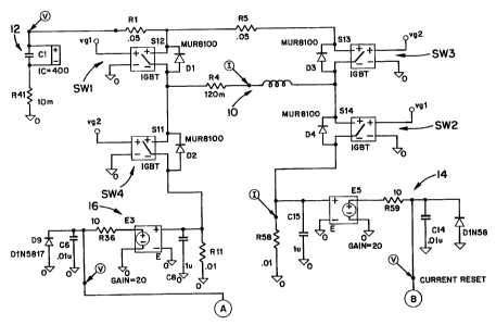
Indicated by reference numeral 10 in Fig. 1 A is a coil installed in a marker
deactivation device and selectively energized for the purpose of generating a
magnetic field
to which magnetomechanical EAS markers are to be exposed for deactivation.
Although only
t 5 one coil is indicated at reference numeral 10, it should be understood
that two or more coils
may be employed, connected in series or in parallel with each other.
Also indicated in the circuitry of Fig. 1 A is a bulk storage capacitor 12.
According to
a preferred embodiment of the invention, the capacitor 12 has a rating of
1,000 microfarads,
although larger or smaller capacitors, or a bank of capacitors, may
alternatively be employed.
Connected between the capacitor 12 and a first terminal of the coil 10 is a
first
transistor switch SW1. A second transistor switch SW2 is connected between a
second
terminal of the coil 10 and ground.
A third transistor switch SW3 is connected between the capacitor 12 and the
second
terminal of the coil 10; and a fourth transistor switch SW4 is connected
between the first
terminal of the coil 10 and ground. In the drawing, all four of the transistor
switches are
shown as being constituted by insulated-gate bipolar transistors (IGBT's);
however, other
types of transistors, such as MOSFET's, may be used. Other kinds of switching
elements may
be employed as alternatives to transistor switches.
A first current sense circuit 14 is connected to the coil 10 by way of switch
SW2. At
times when switch SW2 is in a closed condition, the current sense circuit 14
converts a current
level present in the coil 10 into a voltage level to be provided to a control
circuit that will be
described below. Also shown in Fig. 1 A is a second current sense circuit 16,
connected to the
4
CA 02338849 2001-01-25
WO 00/10143 PCT/US99/17901
coil 10 by way of switch SW4. The current sense circuit 16 provides to the
control circuit a
voltage level which represents the current level in the coil 10 at times when
the switch SW4
is in a closed condition.
As will be seen, the control circuit controls the respective states of the
transistor
switches S W 1 through SW4 such that a sequence of DC pulses, of alternating
polarity, are
applied to the coil 10, with the pulses declining in amplitude over time to
generate a signal
field which substantially degausses the bias element of a magnetomechanical
marker
positioned near the coil.
The control circuit which generates the control signals applied to the
switches SW1
through SW4 is illustrated in Figs. 1 B and 1 C.
Referring initially to Fig. 1 B, the current sense signal output from the
current sense
circuit 14 is applied to the non-inverting input of a first comparator 18.
Also, the current
sense signal output by the current sense circuit 16 is applied to the non-
inverting input of a
second comparator 20.
A circuit indicated at 22 in Fig. 1 B produces an output signal having a
rising ramp
waveform. The rising ramp signal is level shifted and inverted by a circuit 24
to form an
output signal having a declining ramp waveform. The declining ramp signal is
provided in
parallel to the respective inverting inputs of the comparators 18 and 20. The
output signals
of the comparators 18 and 20 are applied to "clear" inputs of a first D-type
flip-flop 26 (Fig.
1 C) and of a second D-type flip-flop 28, respectively. A first clock signal
indicated at 30 is
applied to the "clock" input of the flip-flop 26. A second clock signal,
indicated at 32, is
applied to the "clock" input of the flip-flop 28. In a preferred embodiment of
the invention,
both clock signals are at substantially 500 Hz, and are substantially 180 out
of phase with
each other.
In the case of each of the flip-flops 26, 28, the respective inverted output
thereof is
connected to the "D" input of the respective flip-flop. The non-inverted
output of the flip-flop
26 is provided in parallel as a control signal to the switches SWI and SW2.
The non-inverted
output of the flip-flop 28 is provided in parallel as a control signal to the
switches SW3 and
SW4. Consequently, switches SW 1 and SW2 are effectively ganged together under
control
of flip-flop 26, and switches SW3 and SW4 are effectively ganged together
under control of
flip-flop 28. When the output of flip-flop 26 is at a "high" logic level, the
switches S W 1 and
SW2 are in a closed condition; at all other times switches SW1 and SW2 are
maintained in
5
CA 02338849 2001-01-25
WO 00/10143 PCT/US99/17901
an open condition. When the output of flip-flop 28 is at a "high" logic level,
the switches
SW3 and SW4 are in a closed condition; at all other times switches SW3 and SW4
are
maintained in an open condition.
Operation of the circuit of Fig. 1 will now be described, with reference to
Figs. 2-4.
Figs. 2A and 2B share a common horizontal scale, which is shown explicitly in
Fig.
2A. Fig. 2A illustrates a repeated rising ramp waveform generated by the
circuit 22 of Fig.
1 B. Fig. 2B illustrates a repeated declining ramp signal generated by the
circuit 24 and
applied in parallel to the inverting inputs of the comparators 18 and 20.
Figs. 3A-3E all have a common horizontal scale, which corresponds to a time
period
of about 5 milliseconds (the gradations for the shared horizontal scale are
explicitly shown
only in Fig. 3B).
Fig. 3A shows a waveform indicative of the output of flip-flop 26. The
waveform of
Fig. 3A is a series of brief pulses. Since the output of flip-flop 26 is the
control signal for
switches SWI and SW2, the brief periods during which the signal of Fig. 3A is
at a "high"
logic level correspond to the times when the switches SW 1 and SW2 are in a
closed condition.
At all other times switches SW 1 and SW2 are in an open condition. The timing
at which each
pulse of Fig. 3A begins corresponds to a rising edge of the 500 Hz clock
signal applied to the
flip-flop 26. Consequently, the pulses shown in Fig. 3A begin at intervals of
substantially 2
milliseconds. The timing at which each pulse of Fig. 3A ends is set by a
rising edge of the
output signal of comparator 18, applied to the "clear" terminal of flip-flop
26. The timing of
the output of the comparator 18, in turn, depends on the relationship between
the respective
levels of the declining ramp signal applied to the inverting input of the
comparator 18, and the
current sense signal applied to the non-inverting input of the comparator 18.
During the brief intervals when the output of the flip-flop 26 is at a high
level, the
switches SW I and SW2 are closed, allowing a DC pulse to be applied to the
coil 10 from the
capacitor 12 in the direction from the switch S W 1 to the switch SW2. These
current pulses
are indicated at 40, 42 and 44 in Fig. 3E, which illustrates the signal
waveform of the current
in coil 10, with the current flow direction from switch SW 1 to switch SW2
being taken as the
positive polarity. Corresponding current sense pulses output from the current
sense circuit
14 are indicated at 50, 52 and 54 in Fig. 3C. It will be recalled that these
current sense signal
pulses are provided as input signals to the non-inverting input of the
comparator 18. The
signal trace 56 shown in Fig. 3C corresponds to the declining ramp signal
supplied to the
6
CA 02338849 2001-01-25
WO 00/10143 PCT/US99/17901
inverting input of the comparator 18. The points of intersection of the pulses
50, 52, 54 with
the declining ramp signal trace 56 are indicative of the timings at which the
control signal
pulses of Fig. 3A are terminated by the comparison output signal from the
comparator 18. It
will be recognized that, as the level of the declining ramp signal decreases,
the duration of the
control signal pulses output from the flip-flop 26 decreases, as does the peak
amplitude of the
DC current pulses sequentially applied to the coil 10.
Fig. 3B is indicative of the control signal output from flip-flop 28 to
control the
switches SW3 and SW4. The timings of the beginnings of the pulses shown in
Fig. 3B are
determined by the rising edges of the 500 Hz clock applied to flip-flop 28.
Thus the pulses
in Fig. 3B commence at intervals of 2 milliseconds, and the pulse train shown
in Fig. 3B is
at a 180 phase offset from the pulse train of Fig. 3A. It will also be noted
that, between each
pulse of Fig. 3A and the next succeeding pulse of Fig. 313, there is an
intervening period
which is substantially longer in duration than the respective durations of
either of the pulses.
During the brief intervals when the control signal from the flip-flop 28 is at
a "high"
logic level, the switches SW3 and SW4 are closed, so that a DC current signal
is induced in
the coil 10 from the storage capacitor 12 in the direction from switch SW3 to
switch SW4.
The negative polarity pulses shown in Fig. 3E at 60 and 62 are indicative of
these current
pulse signals. The corresponding current sense voltage levels output from the
current sense
circuit 16 and provided as input signals to the non-inverting input of
comparator 20, are
indicated at 70, 72 in Fig. 3D. In Fig. 3D the trace 56 again represents the
declining ramp
signal, which as noted before is input to the inverting input of the
comparator 20. Thus the
intersections of the pulses 70, 72 with the trace 56 determine the timings of
the ends of the
control signal pulses of Fig. 3B, which in tu.rn control the termination of
the negative-sense
current pulses applied to the coil 10.
Fig. 4 shows, on a more compressed time scale, the current signal level trace
of Fig.
3E. As seen from Fig. 4, a train of DC pulses is applied to the coil 10, the
pulses having
alternating polarities and a decreasing amplitude governed by the level of the
declining ramp
signal applied to the inverting inputs of the comparators 18, 20.
Circuitry for charging the capacitor 12 is not shown in the drawings, but may
be like
that disclosed in above-referenced U.S. Patent No. 5.781,111. In the circuitry
of the'111
patent, the storage capacitor is intermittently isolated from the deactivation
coil, and during
such periods is charged from a power line signal. In the present invention,
alternate ones of
7
CA 02338849 2001-01-25
WO 00/10143 PCT/US99/17901
the periods corresponding to the declining ramp signal may be used for
charging, with the
other periods utilized to generate the pulse trains illustrated in Fig. 4.
It will be recognized that the sequence of declining amplitude, alternating
polarity DC
pulses shown in Fig. 4 provides a magnetic field which will operate to degauss
the bias
magnet of a magnetomechanical EAS marker presented at the coil 10, and without
requiring
relative motion between the marker and the coil. The circuitry illustrated in
Fig. l is expected
to be highly energy efficient, since the duty cycle is quite low. In addition,
the circuitry shown
herein is relatively simple, and should therefore be economical to
manufacture.
Fig. 5 illustrates an alternative to the one coil, four-switch arrangement
shown in Fig.
lA. In the arrangement of Fig. 5, two coils and six switches are provided.
With the
arrangement of Fig. 5, two coils, possibly arranged with orthogonal
orientations (as in an
embodiment shown in Fig. 8 of co-pending patent application serial no.
09/016,175, filed
January 30, 1998, and commonly assigned with the present application), may be
driven in
alternating modes.
Fig. 5 shows the same coil 10 and switches SW1, SW2, SW3 and SW4 as shown in
Fig. 1 A. Also shown in Fig. 5 is a second coil 80, which has one terminal
connected to the
junction of switches SW3 and SW2. Switch SW5 is connected between the storage
capacitor
(not shown in Fig. 5) and the other terminal of coil 80, while switch SW6 is
connected
between the latter terminal of coil 80 and a third current sense circuit,
which is not shown.
All six switches may be transistor switches such as IGBT's.
In the first mode of operation of this embodiment of the invention, switches
SW5 and
SW6 are maintained in an open condition, so that coil 80 is effectively out of
the circuit;
switches SWI through SW4 are operated in the same manner as described above in
connection with Figs. 2-4.
In the second mode of operating this embodiment of the invention, switches SW
1 and
SW4 are maintained in an open condition to effectively remove coil 10 from the
circuit, and
switches SW3, SW6, SW5 and SW2 are operated in like manner to the operations
of switches
SWI through SW4 in the first mode.
Thus, in the first mode of operation, a pulse train like that of Fig. 4 is
applied to coil
10, and in the second mode of operation a like pulse train is applied to coil
80. It will be
understood that the apparatus is to be repeatedly switched between the first
and second modes
of operation at short intervals.
8
CA 02338849 2001-01-25
WO 00/10143 PCT/US99/17901
It is well within the ability of those who are skilled in the art to modify
the control
circuit of Figs. 1 B and 1 C to implement the two modes of operation described
above. -
Various changes in the foregoing deactivation devices and modifications in the
described practices may be introduced without departing from the invention.
The particularly
preferred embodiments of the invention are thus intended in an illustrative
and not limiting
sense. The true spirit and scope of the invention are set forth in the
following claims.
9