Note: Descriptions are shown in the official language in which they were submitted.
CA 02338964 2001-03-O1
HIGH CAPACITY ULTRA-LONG HAUL DISPERSION AND
NONLINEARITY MANAGED LIGHTWAVE COMMUNICATION SYSTEMS
Field of the Invention
The present invention relates to method and apparatus for
transmitting optical signals in high-capacity, long distance,
lightwave communication systems which use Return-To-Zero (RZ)
modulation format and dispersion management.
Background of the Invention
Optical nonlinearities of optical transmission fibers have
become limiting factors for long distance, high capacity
lightwave transmission systems. In an optically amplified
transmission system transmission system, the amplified
spontaneous emission (ASE) noise degrades the signal-to-noise
ratio (SNR), and a higher signal power is then required to
maintain a minimum SNR. However, optical nonlinearities distort
the transmission signal and thus limits the maximum~optical power
that can be launched over the optical transmission line.
It is possible to balance the self-phase-modulation (SPM)
with chromatic dispersion by a proper design of the transmission
pulse waveform as well as the pulse energy. Such nonlinear
pulses are known as "optical solitons". Since the chromatic
dispersion is compensated for by optical nonlinearity, there is
no need to perform dispersion compensation in soliton systems.
In this regard see, for example, U.S. Patent No. 4,558,921 (A.
Hasegawa), issued on December 17, 1985, U.S. Patent No. 4,700,339
(J.P. Gordon), issued on October 13, 1987, and U.S. Patent No.
5,035,481 (L. F. Mollenauer) issued on July 30, 1991.
1
' CA 02338964 2001-03-O1
Although transoceanic soliton transmission is known,
conventional soliton transmission technology has not been
commercialized. One of the major problems with conventional
soliton transmission is timing fitter. A soliton pulse width is
typically approximately 10% of a bit period and there is no
fundamental mechanism that can fix such short pulses in time.
Perturbations such as soliton-soliton interaction, frequency
shift due to the ASE noise, and an acoustic wave generated by a
previous pulse tend to move the pulses out of their original
position as is indicated in U.S. Patent No. 5,710,649 (L. F.
Mollenauer), issued on January 20, 1998. Still further, many
techniques have been used to reduce or eliminate timing fitter as
is described in the book entitled "Optical Fiber
Telecommunications IIIA" by I. P. Kaminow et al., at pages 373-
461 (Academic Press, 1997). All the above techniques, also known
as "soliton control technologies" are typically not cost
effective in many practical applications, and also complicate
system designs.
Recently, a new class of solitons (dispersion managed
solitons) were described in the article entitled "Reduction of
Gordon-Haus timing fitter by periodic dispersion compensation in
Soliton transmission" by M. Suzuki et al., Electronic Letters,
Vol. 31, No. 23, pages 2027-2029, 1995. An article entitled
"Soliton Transmission Using Periodic Dispersion Compensation", by
N. J. Smith et al, in Journal of Lightwave Technology, Vol. 15,
No. 10, pages 1808-1822, 1997, discusses a dispersion managed
soliton (DMS) which has been shown to have a much better
2
CA 02338964 2001-03-O1
performance than a conventional soliton, while at the same time
having inherent desired properties of conventional solitons in
dealing with optical nonlinearities. There are five major
improvements in DMS transmission systems compared to conventional
soliton systems. These five improvements are (a) energy
enhancement wherein it is possible to launch much higher signal
power for a DMS signal than conventional soliton signals, which
improves the system SNR; (b) reduced timing fitter; (c) no
additional soliton control technologies are required; (d) it is
compatible to existing non-return-to-zero (NRZ); and (e) it has
high power and dispersion tolerance.
In an article entitled "1 Tbit/s (100 x 10.7Gbits)
Transoceanic Transmission Using 30nm-Wide Broadband Optical
Repeaters with Aeff-Enlarged Positive Dispersion Slope Fiber and
Slope-Compensating DCF" by T. Tsuritani et al., at pages 38-39 of
Post-Deadline Papers, 25th European Conference on Optical
Communications, 1999, discloses that significant system
performance has been achieved using DMS technology in many
laboratory experiments in terms of both distance and total
capacity. Similar performance has also been demonstrated by many
other such as, for example, the articles entitled "1 Terabits
WDM Transmission over 10,000km" by T. Naito et al., PD2-1, pages
24-25, 25th European Conference on Optical Communication, 1999,
and "1.1-Tb/s (55 x 20-GB/s) DENSE WDM SOLITON TRANSMISSION OVER
3,020-km WIDELY-DISPERSON-MANAGED TRANSMISSION LINE EMPLOYING
1.55/1.58 um HYBRID REPEATERS", by K. Fukuchi et al., PD2-10,
3
' CA 02338964 2001-03-O1
pages 42-43, 25th European Conference on Optical Communication,
1999.
Although previous laboratory experiments have proven the
feasibility of DMS systems for long distance and high capacity
applications, there are many challenges to achieve both
reliability and flexibility such that such DMS system can be used
in a realistic environment. For example, in terrestrial optical
fiber networks, the distance between repeaters or optical
amplifiers can be as long as 130km. Such distances are
significantly longer than those of the previous experiments. The
impacts of the longer repeater spacing are two-fold. First, the
required signal power is typically much higher to overcome the
SNR degradation caused by a required larger amplifier gain.
Second, as a result of the required higher signal power, optical
nonlinearities become more important for long distance
transmission. Another challenge is that there are a variety of
different optical fiber types in existing optical fiber networks.
Optical nonlinearities become even more detrimental for a
transmission line comprising different types of optical fibers.
As for DMS systems, the total capacity is limited not only by the
optical amplifier bandwidth, but also the higher order chromatic
dispersion of the transmission fiber. The situation is even more
difficult when there are several different types of optical
fibers involved. A reliable and cost-effective solution to
higher order chromatic dispersion is one of the major challenges
for high capacity long haul DMS systems. Finally, distance and
capacity are not the only requirements for next generation
4
' CA 02338964 2001-03-O1
optical networks. For example, it is highly desirable to have
the flexibility to place optical add/drop nodes anywhere along an
optical transmission line.
In a dispersion managed soliton (DMS) system, DMS predicts
significant power enhancement which is valid for single channel
propagation. The power enhancement cannot be fully utilized for
multi-channel system since the cross-phase modulation (XPM)
dominates the overall system performance. DMS systems further
require an accurate balance between the self-phase modulation
(SPM) in the transmission fiber and the SPM a dispersion-
compensating fiber which often results in a much smaller system
margin.
It is desirable to provide a high capacity ultra-long haul
dispersion and nonlinearity managed lightwave communication
system which overcomes the problems described hereinabove.
Summary of the Invention
The present invention is directed to method and apparatus
for transmitting optical signals in high-capacity, long distance,
lightwave communication systems which use Return-To-Zero (RZ)
modulation format and dispersion management.
Viewed from an apparatus aspect, the present invention is
directed to an optical transmission system. The optical
transmission system comprises a transmitter terminal and an
optical transmission line. The transmitter terminal comprises a
plurality of return-to-zero (RZ) transmitters and a multiplexing
arrangement. Each of the plurality of return-to-zero (RZ)
transmitters is adapted to receive a separate channel input
5
CA 02338964 2001-03-O1
signal and to generate therefrom a corresponding forward error
correction (FEC) modulated output signal in a separate
predetermined channel frequency sub-band of an overall frequency
band which includes a predetermined channel separation from an
adjacent channel frequency band generated by another RZ
transmitter. The multiplexing arrangement multiplexes the
plurality of the predetermined channel frequency sub-bands from
the plurality of RZ transmitters into separate groups of
frequency bands where the groups of frequency bands have a
predetermined band-gap separation therebetween wherein each group
of frequency bands has a predetermined separate pre-chirp
introduced before being multiplexed with all other groups of
frequency bands into a single multiplexed output signal. The
optical transmission line has an input coupled to an output of
the multiplexing arrangement and is subdivided into a plurality
of optical transmission line sections. The optical transmission
line comprises a plurality of Raman amplifiers and at least one
dispersion compensating line amplifier (DCLA). One of the
plurality of Raman amplifiers is located at the end of each
optical transmission line section and is adapted to receive at an
input thereof the single multiplexed output signal propagating in
an associated transmission line section and to combine a
predetermined Raman pump power signal into the optical
transmission line section in an opposite direction to the
received single multiplexed output signal to generate at an
output thereof an output signal which is Raman amplified for
increasing a path averaged optical power without increasing
6
CA 02338964 2001-03-O1
nonlinear degradation. The at least one DCLA is coupled to an
output of a Raman amplifier at the end of a predetermined group
of optical transmission line sections. The DCLA is adapted to
introduce dispersion compensation for the single multiplexed
output signal, and to introduce separate high-order dispersion
compensation for each of the groups of frequency bands therein.
Viewed from a method aspect, the present invention is
directed to a method of transmitting signals in an optical
transmission system. The method comprises the steps of:
(a) receiving each channel input signal of a plurality of channel
input signals in a separate one of a plurality of return-to-zero
(RZ) transmitters, and generating therefrom a corresponding
forward error correction (FEC) modulated output signal in a
separate predetermined channel frequency sub-band of an overall
frequency band which includes a predetermined channel separation
from an adjacent channel frequency band generated by another RZ
transmitter; (b) multiplexing the plurality of the predetermined
channel frequency bands from the plurality of RZ transmitters
into separate groups of frequency bands where the groups of
frequency bands have a predetermined band-gap separation
therebetween, wherein each group of frequency bands has a
predetermined separate pre-chirp introduced before being
multiplexed with all other groups of frequency bands into a
single multiplexed output signal; (c) receiving the single
multiplexed output signal in an optical transmission line which
is subdivided into predetermined optical transmission line
sections; (d) receiving the single multiplexed output signal
7
CA 02338964 2001-03-O1
propagating in each optical transmission line section by a
separate Raman amplifier which combines a predetermined Raman
pump power signal into the optical transmission line section in
an opposite direction to the received single multiplexed output
signal to generate an output signal which is Raman amplified for
increasing a path averaged optical power without increasing
nonlinear degradation; and (e) introducing dispersion
compensation from a dispersion compensating line amplifier (DCLA)
into the single multiplexed output signal from an output of a
Raman amplifier at the end of a predetermined group of optical
transmission line sections for providing separate high-order
dispersion compensation for each of the groups of frequency bands
in said single multiplexed output signal.
The invention will be better understood from the following
more detailed description taken with the accompanying drawings
and claims.
Brief Description of the DrawincLs
FIGS. lA and 1B show a block diagram of an exemplary ultra-
long haul lightwave transmission system in accordance with the
present invention;
FIG. 2 shows a block diagram of an exemplary return-to-zero
transmitter for use in a transmitting terminal of the exemplary
ultra-long haul lightwave transmission system of FIGS. lA and 1B
in accordance with the present invention;
FIG. 3 shows a block diagram of a Raman amplifier for use in
a optical transmitting fiber of the exemplary ultra-long haul
8
CA 02338964 2001-03-O1
lightwave transmission system of FIGS. lA and 1B in accordance
with the present invention;
FIG. 4 graphically shows an exemplary Raman Gain
characteristic shape obtainable from the Raman amplifier of FIG.
3 in accordance with the present invention;
FIG. 5 shows a block diagram of an optical line amplifier
for use in a optical transmitting fiber of the exemplary ultra-
long haul lightwave transmission system of FIGS. lA and 1B in
accordance with the present invention;
FIG. 6 shows a block diagram of a dispersion compensating
line amplifier for use in a optical transmitting fiber of the
exemplary ultra-long haul lightwave transmission system of FIGS.
lA and 1B in accordance with the present invention;
FIG. 7 shows a block diagram of an exemplary return-to-zero
receiver for use in a receiving terminal of the exemplary ultra-
long haul lightwave transmission system of FIGS. lA and 1B in
accordance with the present invention;
FIG. 8 graphically shows a plot for system performance at
different pulse widths for an exemplary system in accordance with
the present invention;
FIG. 9 graphically shows a plot of channel power for an
optimization of channel power in an exemplary system in
accordance with the present invention;
FIG. 10 graphically shows a contour plot for path average
dispersion for one section of a optical transmission fiber in
accordance with the present invention;
9
CA 02338964 2001-03-O1
FIG. 11 graphically shows a plot of channel loading penalty
using a frequency band approach in accordance with the present
invention;
FIG 12 shows a graph for dispersion management of an
exemplary system for an exemplary transmission line route of
2950km consisting of mixed optical fibers in accordance with the
present invention; and
FIG. 13 graphically shows a plot for an exemplary system
performance of predetermined hybrid fiber types after
transmitting optical signals through a distance of 2950km through
the mixed fibers in accordance with the present invention.
Detailed Description
The present invention uses three enabling technologies to
overcome the practical challenges found in the prior art. These
three enabling technologies are: (a) a return-to-zero (RZ)
modulation format, (b) a wavelength band structure for each of
bandwidth, dispersion, and nonlinearity management, and (c)
distributed Raman amplification. None of the three enabling
technologies by itself can be used to realize a required system
performance for a high capacity, long distance lightwave
transmission system. The description which follows describes the
problems that must be solved and how the above-mentioned three
technologies are optimally used to achieve the required system
performance.
Since optical nonlinearities and amplifier noise are the two
major limitations for ultra-long haul optical transmission, the
utilization focus of the above-mentioned three different
CA 02338964 2001-03-O1
technologies is to minimize the impact of optical nonlinearities
while maximizing the optical signal-to-noise ratio (OSNR). There
are four major optical nonlinearities in single mode transmission
fibers. They are (a) self-phase modulation (SPM) which refers to
a single channel nonlinear effect resulting from an optical Kerr
effect, (b) cross-phase modulation (XPM) which is a multi-channel
nonlinear effect resulting from the optical Kerr effect, (c)
four-wave mixing (FWM) which is a coherent multi-channel
nonlinear effect resulting from the optical Kerr effect, and (d)
stimulated Raman scattering (SRS) which is a multi-channel
nonlinear effect resulting from an interaction between laser
radiation and molecular vibrations.
It is found that a return-to-zero (RZ) modulation format is
very effective in minimizing SPM [described in nonlinearity (a)
above] if a dispersion map is optimized. There exists a certain
range of optimum pulse width which allows the design of a an RZ
transmission system using available commercial transmitter
components. The optimum pulse width is also affected by choices
of frequencies for channel spacings.
With regard to cross-phase modulation (XPM) described for
nonlinearity (b) above, XPM is the most difficult optical
nonlinearity to manage. In accordance with the present
invention, three techniques are used to minimize XPM. First, the
transmission bandwidth is divided into frequency bands with
predetermined band gaps between adjacent bands to aid in limiting
the XPM degradation to a tolerable level. A channel loading
penalty due to XPM decays much faster than with uniform channel
11
CA 02338964 2001-03-O1
allocation or non-band techniques. Second, the use of backward
distributed Raman amplification helps to increase the path
averaged optical powers without increasing nonlinear degradation.
This makes it possible to maintain a required OSNR while reducing
the channel launching power. Third, as is described hereinbelow,
the technique for higher dispersion management helps to randomize
a phase relationship among different frequency bands. This
reduces the worst case scenario of channel realignment due to
periodic dispersion compensation.
Four-wave mixing (FWM), described for nonlinearity (c)
above, is minimized by channel frequency allocation as well as
distributed Raman amplification for the reasons expressed
hereinbefore for the advantages of channel frequency allocation
and distributed Raman amplification. The impact of stimulated
Raman scattering (SRS), described for nonlinearity (d) above, is
two-fold. SRS causes energy transfer among channels which
generates a dynamic power tilt, and it gives rise to statistical
channel-to-channel cross-talk. In accordance with the present
invention, the dynamic power tilt problem is. solved by using
automatic band power equalization inherent in the structure of
higher order dispersion management. Channel-to-channel Raman
cross-talk is substantially reduced by distributed amplification
due to the use of a lower launching power.
The ultimate transmission distance is determined by optical
nonlinearities and optical amplifier noise. It is possible to
control the growth of amplifier noise by placing optical
amplifiers at closer spacings, just as in submarine optical
12
CA 02338964 2001-03-O1
transmission systems. However, system designers do not have this
freedom in designing terrestrial transmission systems. Even
though the impacts of optical nonlinearities have been minimized,
forward error correction (FEC) is required to extend the
transmission distance beyond the nonlinearity limits. The
effectiveness of FEC is affected by the extent of nonlinearity
management. On the other hand, an out-of-band FEC technique
requires higher bit rate or shorter pulses, which also affect the
nonlinearity management.
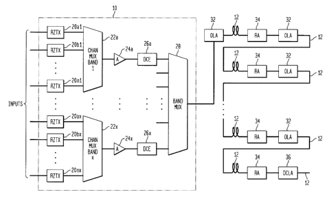
Referring now to FIGS. lA and 1B, there is shown a block
diagram of an exemplary ultra-long haul lightwave transmission
system in accordance with the present invention. FIG. lA shows a
block diagram of an exemplary transmitting terminal 10 (shown
within a dashed-line rectangle) and an exemplary ultra-long haul
optical transmission line 12 in accordance with the present
invention. FIG. 1B shows a block diagram of a remaining portion
of the exemplary ultra-long haul optical transmission line 12
shown in FIG. lA, and an exemplary receiving terminal 14 (shown
within a dashed-line rectangle) for receiving the optical signals
from the transmitting terminal 10 in accordance with the present
invention.
The exemplary transmitting terminal 10 comprises a plurality
of X groups of N return-to-zero transmitters (RZTX) 20a-20n each
(of which only the group of RZTXs 20a1-20n1 for group 1 and the
group of RZTXs 20ax-20nx are shown), a plurality of X channel
multiplexers (CHAN MUX BAND) 22a-22x (of which only channel
multiplexers 22a and 22x are shown), a plurality of X low power
13
CA 02338964 2001-03-O1
optical amplifiers (A) 24a-24x (of which only amplifiers 24a and
24x are shown), a plurality of X dispersion compensating elements
(DCE) 26a-26x (of which only DCEs 26a and 26x are shown), and a
band multiplexer (BAND MUX) 28. Each of the RZTXs 20a1-20n1
receives a separate input signal and converts the associated
input signal into a separate output signal in a separate
frequency band of an overall first frequency band (BAND 1).
Similarly, each of the RZTXs 20ax-20nx receives a separate input
signal and converts the associated input signal into a separate
output signal in a separate frequency band of an overall last
frequency band (HAND X). It is to be understood, that although
each group of RZTXs is shown as comprising n RZTXs 20a-20n, the
number "n" in each group can comprise a different number where in
a practical arrangement an equal number of RZTXs 20a-20n are not
available for each of the X groups of RZTXs 20a-20n. The channel
multiplexers 22a and 22x receive the outputs from the RZTXs 20a1-
20n1 and 20ax-20nx, respectively, and multiplex the received
signals within the proper frequency band slots of the respective
overall frequency bands 1 and X and transmits a separate single
output signal. The combined signals in the first overall
frequency band (BAND 1) from the first channel multiplexer (CHAN
MUX HAND 1) 22a are transmitted through a low power optical
amplifier 24a, which amplifies the first overall frequency band
signal to a predetermined level, and then a dispersion
compensating element 26a that adds a predetermined chirp
(dispersion value) to the associated first overall frequency
band. Similarly, the combined signals in the last overall
14
CA 02338964 2001-03-O1
frequency band (BAND X) from the last channel multiplexer (CHAN
MUX BAND X) 22a are transmitted through a low power optical
amplifier 24x, which amplifies the last overall frequency band
signal to a predetermined level, and then to a dispersion
compensating element 26x that adds a predetermined chirp
(dispersion value) to the associated last overall frequency band.
The output signals from each of the dispersion compensating
elements 26a-26x are received at separate inputs of the band
multiplexer 28 where the plurality of X overall frequency bands
are combined into a single output signal from the transmitting
terminal 10 for transmission over an ultra-long haul optical
transmission line 12.
In the transmitting terminal 10, the overall transmission
frequency bandwidth is divided into many smaller frequency bands
1-X with predetermined gaps therebetween between the adjacent
frequency bands. Each frequency band 1-X contains a
predetermined number °n~~ of channels obtained from the associated
RZTXs 20a-20n with predetermined channel spacings.
The ultra-long haul optical transmission line 12 comprises a
plurality of optical line amplifiers (OLA) 32, a plurality of
backward-pumped Raman amplifiers (RA) 34, and at least one
dispersion compensating line amplifier (DCLA) 36. Each section
of the optical transmission line comprises one of the optical
line amplifier (OLA) 32 at the beginning which can comprise an
Erbium-doped fiber amplifier (EDFA), and one of the backward-
pumped Raman amplifiers (RA) 34 at the end of the optical
transmission line section. After a predetermined number of
CA 02338964 2001-03-O1
optical transmission line sections, the OLA 32 is replaced by one
of the dispersion compensating line amplifier (DCLA) 36. The
functionalities of the DCLA 36 are mainly two-fold. The DCLA 36
compensates for higher-order chromatic dispersion, and equalizes
the band power. The DCLA 36 also provides the benefits of
reducing the cross-phase modulation (RPM) among adjacent bands.
The location of the DCLA 36 along the optical transmission line
12 can be flexible, which allows network designers to place DCLAs
36 at convenient locations. After the DCLA 36, the structure of
the optical transmission line 12 periodically repeats itself
until reaching the final destination at the receiving terminal 14
shown in FIG. 1B.
As shown in FIG. 1H, in the last optical transmission line
section, the optical signals pass through the final backward-
pumped Raman amplifier (RA) 34, and are received by the receiving
terminal 14. The receiving terminal 14 comprises a pre-amplifier
(PA) 40, a broadband dispersion compensator (DC) 42, a band
demultiplexer (HAND DEMUR) 44, a plurality of post dispersion
compensating (POST DC) modules 46a-46x (of which only Post DCs
46a and 46x are shown), a plurality of channel band
demultiplexers (CHAN BAND DEMUR) 48a-48x (of which only CHAN BAND
DEMUXs 48a and 48x are shown), and a plurality of (N)(X) return-
to-zero receivers (RZRX) 50a-50n (of which only RZRX receivers
50a1-50an and 50n1-50nx are shown for bands 1 and X,
respectively).
The band demultiplexer 44 functions to separate each of the
overall frequency bands 1-X received from the optical
16
CA 02338964 2001-03-O1
transmission line 12 into individual outputs for propagation over
optical fiber paths 45a-45x, respectively, of which only optical
fiber paths 45a and 45x are shown with included devices. A post
dispersion compensating module 46a receives the signals in
frequency band 1 via optical fiber path 45a and provides post
dispersion compensation for frequency band 1. Similarly, a post
dispersion compensating module 46x receives the signals in
frequency band X via optical fiber path 45x and provides post
dispersion compensation for frequency band X. Each of the
plurality of channel band demultiplexers 48a-48x receives the
output signals from a separate associated one of the plurality of
post dispersion compensating modules 46a-46x, and further
demultiplexes the received frequency band (e. g., frequency band
1) into the associated individual channels for transmission over
a separate output path. Each of the channels 1-n of frequency
band 1 from channel band demultiplexer 48a is coupled to an
corresponding separate one of the plurality of RZRXs 50a1-50n1,
and each of the channels 1-n of frequency band X from channel
band demultiplexer 48x is coupled to an corresponding separate
one of the plurality of RZRXs 50ax-50nx.
Referring now to FIG. 2, there is shown a block diagram of
an exemplary return-to-zero transmitter (RZTX) 20 (shown within a
dashed line rectangle) for use in the transmitting terminal 10 of
the exemplary ultra-long haul lightwave transmission system of
FIGS. lA and 1H in accordance with the present invention. The
RZTX 20 comprises an Forward Error Correction (FEC) encoder 60, a
modulation driver 62, a pulsed laser driver 64, a short pulse
17
CA 02338964 2001-03-O1
laser source 66, and an optical modulator (MODULATOR) 68. Input
electronic data and clock signals are received at separate inputs
of the FEC encoder 60 which provides an encoded data output
signal for transmission to the modulator driver 62. The
modulation driver 62 uses the FEC encoder 60 output signal to
drive the optical modulator 68. The electronic clock signal is
also received at an input of the pulsed laser driver 64 which is
used to drive the short pulse laser source 66 to provide a
corresponding optical laser output signal. The short pulse laser
source 66 can be implemented by any suitable laser source as, for
example, a Lithium-Niobate modulator, and electro-absorption
modulator, or directly by a mode-locked short pulse laser. The
optical modulator 68 modulates the optical output signal from the
short pulse laser source 66 with the FEC encoded output signal
from the modulation driver 62 to generate an return-to-zero (RZ)
optical data output signal from the RZTX 20.
Referring now to FIG. 3, there is shown a block diagram of a
Raman amplifier (RA) 34 (shown within a dashed line rectangle)
for use in a optical transmitting fiber 12 of the exemplary
ultra-long haul lightwave transmission system of FIGS. lA and 1B
in accordance with the present invention. The Raman amplifier 34
comprises a wavelength division multiplexer (WDM) 70, a plurality
of n Raman pump lasers (KAMAN PUMP) 72a-72n (of which only Kaman
pump lasers 721, 72b, and 72n in FIG. 3 are shown), and a pump
laser combiner (COMB.) 74. The number of Kaman pump lasers 72a-
72n, as well as the pump wavelengths therefrom, is determined by
the types of fibers of the optical transmission fiber 12 and the
18
CA 02338964 2001-03-O1
required amplifications. The combined output from the pump laser
combiner 74 is coupled into the optical transmission line 12 in
the opposite direction to the received input signals by the WDM
70.
Referring now to FIG. 4, there is shown a graph of Gain in
dB (decibels) on the Y-axis versus Wavelength in nanometers (nm)
on the X-axis of an exemplary Raman Gain characteristic shape for
various channels obtainable from the Raman amplifier of FIG. 3 in
accordance with the present invention. The exemplary Raman Gain
characteristic shape of FIG. 4 is obtained using a transmission
fiber 12 which is a non-zero dispersion-shifted fiber (NZDSF)
with a length of 100km, a signal loss of 0.22dB/km, a pump loss
of 0.3dB/km, and two pump lasers 72 with a total pump power of
247.4 mW. The backward distributed Raman amplifications have the
benefits of optical signal-to-noise ratio (OSNR) enhancement and
negligible nonlinear degradations. Due to the attenuation of the
optical fiber 12, the signal power near the end of the
transmission fiber 12 is orders of magnitude lower than that at
the input. Some moderate amplification near the end of the
transmission fiber 12 will not increase the signal power to the
nonlinear regime. On the other hand, the path averaged signal
power is greatly enhanced so that the overall noise build-up of
the transmission line 12 is suppressed. The selection of the
Raman gain is determined by both nonlinear degradation and extra
noise addition due to the Raman amplification. After Raman
amplification, the output signals from the Raman amplifier 34 of
19
CA 02338964 2001-03-O1
FIG. 3 are coupled into the line amplifiers 34 of a next section
of the transmission line 12.
Referring now to FIG. 5, there is shown a block diagram of
an exemplary optical line amplifier (OLA) 32 (shown within a
dashed line rectangle) for use in a optical transmitting fiber 12
of the exemplary ultra-long haul lightwave transmission system of
FIGS. lA and 1B in accordance with the present invention. The
exemplary optical line amplifier 32 comprises a serial
arrangement of a low noise pre-amplifier (PA) 80, such as an
Erbium-doped fiber amplifier (EDFA), a gain equalization filter
(GAIN EQUAL. FLT.) 82, an optional broadband dispersion
compensator 84 (shown within a dashed line rectangle), and a
boost amplifier (BA) 86. The gain equalization filter 82
functions to equalize gain variations resulting from a Raman
amplifier 34 at the end of a prior section of the transmission
line 12, the transmission fiber 12 itself, the pre-amplifier 90,
and the boost amplifier 85 (shown in FIG. 5) in the prior optical
line amplifier 32. The broadband dispersion compensator 84 is
optional depending on the types of the transmission fibers used
in the transmission lines 12. The broadband dispersion
compensator 84 is required for standard non-dispersion shifted
fibers that have high chromatic dispersion at the transmission
wavelength, while it is not required for the non-zero dispersion-
shifted fibers (NZDSF) .
Referring now to FIG. 6, there is shown a block diagram of
an exemplary dispersion compensating line amplifier (DCLA) 36
(shown within a dashed line rectangle) for use in a optical
CA 02338964 2001-03-O1
transmitting fiber 12 of the exemplary ultra-long haul lightwave
transmission system of FIGS. lA and 1B in accordance with the
present invention. The dispersion compensating line amplifier
(DCLA) 36 comprises a pre-amplifier (PA) 90, a gain equalization
filter (GEF) 92, a broadband dispersion compensator (HDC) 94, a
band demultiplexer 96, a plurality of X dispersion compensating
modules (DCM) 98a-98x (of which only DCMs 98a, 98b, and 98x are
shown), a plurality of X band power equalizers (BPE) (of which
only HPEs 99a, 99b, and 99x are shown), a band multiplexer (BAND
MUX) 100, and a boost amplifier (BA) 102. The dispersion
compensating line amplifier 36 replaces an optical line amplifier
32 after a predetermined sections of the optical transmission
line 12. The arrangement of the pre-amplifier (PA) 90, gain
equalization filter (GEF) 92, and broadband dispersion
compensator (BDC) 94 is similar to that found for the PA 80, GEF
82, and BDC 84 of the optical line amplifier (OLA) 32 of FIG. 5,
but differs in that a higher order of dispersion compensation is
provided by the BDC 94. The output power of the pre-amplifier 90
is designed to be small so that nonlinearities of the BDC 94 are
insignificant. Another difference between the DCLA 36 and the
OLA 32 is that the BDC 94 is required regardless of the fiber
types found in the optical transmission line 12.
The output of the HDC 94 is received in the band
demultiplexer 96 which divides the overall received frequency
band into the X frequency bands therein and outputs the 1-X
frequency bands over separate optical paths 97a-97x (of which
only paths 97a, 97b, and 97x of FIG. 6 are shown). Optical path
21
CA 02338964 2001-03-O1
97a receives the frequency band 1 and includes a serial
arrangement of the dispersion compensating module (DCM) 98a and
the band power equalizer (BPE) 99a. The DCM 98a includes a
predetermined dispersion value which is specific to the frequency
band 1. The combination of the BDC 94 and the DCM 99a makes it
possible to design the accumulated dispersion value for frequency
band 1 to a predetermined value. Each of the DCMs 98b-98x and
the associated BPEs 99b-99x function in a similar manner for the
associated frequency bands 2-X, respectively. Due to the higher-
order dispersion, or dispersion slope of the transmission fiber
12 and the BDC 94, the accumulated dispersion of each of the
frequency bands 1-X will differ. Using a separate DCM 98a-98x
for each of frequency bands 1-X negates this difference and
provides a flexible mechanism for dispersion management for any
type of optical fiber that is used for optical transmission fiber
12. The output of each of the DCMs 98a-98x is coupled to a
separate associated on of the BPEs 99a-99x which can be, for
example, an adaptive variable attenuator. The output from each
of the BPEs 99a-99x is coupled to a separate input of the band
multiplexer 100 where the 1-X frequency band signals are combined
into a single output signal which is amplified by the boost
amplifier 102 to a predetermined value. The implementation of
the DCLA 36 can vary depending on other considerations such as
cost, size, and loss. For example, the band multiplexer 100 and
the band demultiplexer 96 can by formed from dielectric thin film
filters, or an interleaver and filter combination.
22
CA 02338964 2001-03-O1
Referring now to FIG. 7, there is shown a block diagram of
an exemplary return-to-zero receiver (RZRX) 50 (shown within a
dashed line rectangle) for use in a receiving terminal 14 of the
exemplary ultra-long haul lightwave transmission system of FIGS.
lA and 1B in accordance with the present invention. The RZRX 50
comprises an optical automatic gain control (OAGC) unit 110, a
standard linear channel comprising a high-speed PIN diode (PIN)
112, a low noise amplifier (LNA) 114, and a low-pass filter
(FILTER) 116. The RZRX 50 further comprises a clock/data
recovers (CDR) unit 118, a forward error correction (FEC) decoder
120, a peak power detector (PEAK DETECTOR) 122, a OAGC feedback
mechanism (OAGC FEEDBACK) 124, and an OAGC driver 126. An
associated incoming optical channel signal is received in the
OAGC unit 110 and amplified in an EDFA therein, and then coupled
into the high-speed PIN diode 112 to complete a conversion of the
received optical signal into a corresponding electrical signal
output signal. The LNA 114 amplifies the electrical output
signal from the PIN diode 112 and passes it through the low-pass
filter 116. The filtered output signal is transmitted to the CDR
118 and the peak power detector 122.
The CDR 118 recovers the clock and data signal from the
received channel signal and provides them as an input to the FEC
decoder 120. The FEC decoder corrects for any transmission
errors in the data signal using the FEC information, and provides
the corrected data signal as an output from the RZRX 50. The
output of the peak power detector 122 has a predetermined
bandwidth and is used as a feedback signal to the OAGC feedback
23
CA 02338964 2001-03-O1
unit 124 and, in turn, the OAGC driver 126. The OAGC driver 126
provides a feedback signal to the OAGC unit 110 which is used to
control the EDFA pump current so that the peak power at the CDR
118 is a fixed value.
There are four important system parameters that have the
biggest impact on system performance. These are (a) pulse width,
(b) values of pre-chirp, (c) path averaged dispersion, and (d)
channel power. Since the bit error rate (BER) or Q factor are
the ultimate indicator for system performance, Q or BER is used
to optimize the system performance. Since Q is a highly
nonlinear function of not only the four parameter mentioned
hereinabove, but also many other system parameters, a large
number of system simulations are required so that a global
optimization is achieved. An example of multidimensional Q
mapping are summarized as follows.
In an design for a exemplary system to describe the present
invention, it is assumed that there are a total of 56 channels
grouped into 14 bands with each band comprising four channels
with a channel separation of 50 GHz. Although an information bit
rate is 10 Gbit/s, the actual bit rate is increased to 12.12
Gbit/s due to extra bandwidth required from the FEC encoder 60
shown in FIG. 2. The bandgap is 150 GHz. The transmission fiber
12 is the standard non-dispersion shifted fiber (NDSF) with a
span length of 100km. The Raman gain after gain equalization is
8dB.
Referring now to FIG. 8, there is graphically shown a plot
for an optimization of pulse width for improved system
24
CA 02338964 2001-03-O1
performance with different pulse widths in picoseconds (ps) shown
along the horizontal axis versus Q in decibels (dB) along the
vertical axis for the exemplary system. When the pulse width is
shorter than 20ps, the bandwidth of each channel is so large that
significant spectral overlapping occurs between adjacent
channels, which gives rise to system degradation. For pulse
widths larger than 35ps, a "walk-off~~ distance and the dispersion
length increases, giving rise to a higher nonlinear penalty. For
the hereinabove described exemplary system, a pulse width of
around 25ps is found to be an optimal value.
Referring now to FIG. 9, there is shown a plot of channel
power in units of dBm (decibels/milliwatt) in FIG. 9 along the
X-axis versus Q in dB along the Y-axis for the exemplary system.
For determining optimization of channel power, the amplifier
noise dominates for a channel power below 2dBm, and nonlinearity
dominates for a channel power greater than 5dBm. Therefore, the
optimal channel power for the above exemplary system is around 2-
4 dHm.
Referring now to FIG. 10, there is graphically shown a
contour plot for path average dispersion in units of ps/nm/km
along the X-axis versus pre-chip in a unit normalized value on
the Y-axis for one section of the optical transmission fiber 12.
Q contours are plotted in 1dB intervals. The numbers 11-19
provided for the various contour lines in FIG. 10 in 1dB
increments and represent corresponding Q factor values which are
monitor system performance. There is a 1:1 correspondence
between the Q factor and the bit error rate (BER). Therefore, if
CA 02338964 2001-03-O1
the Q factor is 18 the BER is 10-15. There is a quasi-linear
relationship between the pre-chirp and the average dispersion.
The optimum combination of pre-chirp and average dispersion is
when the pre-chirp = 0.4, and the average dispersion = 0.3
ps/nm/km. There is a large available margin around the optimum
point so that the 1dB range for pre-chirp is from 0.26-0.55,
while for the average dispersion it is from 0.15-0.5. It is
shown that the exemplary system has a significant tolerance to
both pre-chirp and average dispersion. Since the optimization is
done using multiple channels, the results are different from
those of dispersion managed soliton (DMS) systems. The channel
power is selected in such a way that the system behavior is
quasi-linear. The impacts of self-phase modulation (SPM), cross-
phase modulation (XPM), four-wave mixing (FWM), and Raman effects
are minimized in the present invention in such a manner that the
total system characteristics are similar to those of linear
systems. There are fundamental difference between the present
inventive system and prior art return-to-zero (RZ) systems such
as dispersion-managed soliton (DMS) systems. For example, DMS
predicts significant power enhancement, which is valid for single
channel propagation. It further requires accurate balance
between the SPM in a transmission fiber and SPM in a dispersion
compensating fiber, which often results in a much smaller system
margin. In accordance with the present invention, the power in
the dispersion compensating elements of (a) the broadband
dispersion compensator (BDC) 84 and 94 in the optical line
amplifiers 32 and the transmitter terminal 14, and (b) the
26
CA 02338964 2001-03-O1
dispersion compensating modules (DCM) 98a-98x in the dispersion
compensating line amplifier 36 are designed to be smaller than
the nonlinear threshold. Therefore, the spectral broadening due
to SPM is balanced by a proper design of the pre-chirp. This
approach has an advantage over DMS systems in that it enlarges
the system margin as is shown in FIG. 10. Another advantage is
that it allows a system designer to deal with any types of
transmission fibers using the same principles.
Referring now to FIG. 11, there is graphically shown a plot
of channel loading penalty using a frequency band approach where
the channel number (Channel #) is shown along the X-axis and Q in
units of dB (decibels) are shown along the Y-axis for a cross-
phase modulation (XPM) effect. The band structure has an
advantage of minimizing the nonlinear channel-to-channel
interaction which is always a big concern for network designers.
Scalability provides significant economic and network flexibility
advantages. From the plot of FIG. 11, the nonlinear degradation
is limited to a few channels (e.g., channels 4-9) since they are
outside an allowable channel loading penalty-of 0.5 dB. The
total channel loading penalty is controlled to within 0.5 db, and
the absolute values of Q are lower in value than found, for
example, in FIGS. 8 and 9 since the loss in a transmission line
section is much higher (25dB) and the distance is 3200km.
Referring now to FIG 12, there is shown a graph of
propagation distance in kilometers (km) along the X-axis versus
Time in picoseconds (ps) along the Y-axis for an exemplary
transmission line route of 2950km consisting of mixed optical
27
CA 02338964 2001-03-O1
fibers designated LS and TW. Both of the LS and TW type optical
fibers are commercial non-zero dispersion-shifted fibers (NZDSF).
For the exemplary system described hereinabove, there are three
sections of the LS type fiber and two sections of the TW type
fiber shown above the graph. The length of each box at the top
of FIG. 12 indicated the locations of the sites of the DCLAs 36
along the optical transmission line 12. The pre-chirp and
average dispersion is optimized according to the design rules of
the present invention. The contour of the plot indicates the
evolution of pulse intensity along the transmission line 12.
Although the optical fiber characteristics change dramatically at
the interfaces of the different fibers (LS and TW), the pulse
dynamics shown by the contours in the graph manages to evolve
smoothly.
Referring now to FIG. 13, there is graphically shown an
exemplary system performance of the hybrid fiber types after
transmitting signals through a distance of 2950km in the mixed
fibers of FIG. 12. The X-axis indicates the Frequency band
number, and the Y-axis indicates Q in dH. Since a forward error
correction (FEC) threshold is approximately lOdB, there is a
significant system margin at a distance of nearly 3000km. The
pre-chirp is approximately 0.5, the average dispersion is
approximately 0.25ps/nm/km, and the channel power is 0 dBm. The
plot 130 represents values for TW plus LS type optical fibers
while the plot 132 represents values for an FEC limit.
In summary, as a result of proper management of both optical
nonlinearities such as self-phase modulation (SPM), cross-phase
28
CA 02338964 2001-03-O1
modulation (XPM), four-wave mixing (FWM), stimulated Raman
scattering, and higher-order chromatic dispersion, a lightwave
system can be designed with the following advantages. The system
can provide ultra-long haul transmission over arbitrary single
mode transmission fibers, or mixed fiber types, without the use
of electronic regenerators. The system can provide flexible
channel/band add/drop capability in the sense that an arbitrary
number of channels can be dropped or added at arbitrary locations
along an optical transmission line 12. The present invention
provides a scalable network design that is enabled by a
dispersion management technique. Since the chromatic dispersion
is managed on a link-by-link basis, the transmission is not
distance-dependent, which makes the network scalable. Finally, a
scalable transmission capacity is enabled by a wavelength
management technique. The three enabling technologies used to
obtain the present invention are (a) a return-to-zero (RZ)
modulation format, (b) a wavelength band structure for bandwidth
management, dispersion management, and nonlinearity management,
and (c) distributed Raman amplification. The wavelength
bandwidth structure includes the transmission multiplexing
technique, the structure of the dispersion compensating line
amplifier (DCLA) 36 for higher-order dispersion management, and
the demultiplexing in the receiver terminal 14.
It is to be appreciated and understood that the specific
embodiments of the present invention described hereinbefore are
merely illustrative of the general principles of the invention.
29
CA 02338964 2001-03-O1
Various modifications may be made by those skilled in the art
which are consistent with the principles set forth.