Note: Descriptions are shown in the official language in which they were submitted.
CA 02339498 2001-03-05
,BERG2458/C2343
PATENT
MODULAR ELECTRICAL CONNECTOR
FIELD OF THE INVENTION
The present invention relates in general to a high density modular electrical
connector aid, more particularly, to a self centering modular electrical
connector which can
, be readily adapted to different contact counts and configurations.
BACKGROUND OF THE INVENTION
An interface connector is used to connect integrated circuit.(IC) chips and IC
chip carriers to known circuit boards 'or the like. IC chips and IC chip
cariiers.typically have
a plurality of pins or leads in an array on a surface thereof. The pins are
received by
associated passages in an interface connectorwhich is then mounted to a
circuit board, thereby
putting the IC chips and IC chip carriers in electrical contact with the
circuit board.
An adequate interface connector between an IC chip and other circuitry
continues to be a challenge. The number of closely spaced leads which come
from the chip
must be able to interface in a relatively high density configuration. However,
the wide variety
of chip configurations that are available does not always lend itself to
making a uniform
connector in that there may be varying numbers of leads and various arrays of
leads. The
known connectors have generally been useful only for single IC chip
configurations and are
not readily adaptable for expansion and/or revision. Typical limitations to
area array
components include coefficient of thermal expansion (CTE) mismatch,
coplanarity or mold-
2 0 alSility problems (which is the ability to repeatably manufacture a
component using a molding
CA 02339498 2001-03-05
' ~BERG2458/C2343 - 2 - PATENT
process such as thermoplastic molding), and high mating forces and component
alignment.
Regarding the problem of CTE mismatch, area array components such as
connectors, devices, and packages, are limited in size based on the materials
that form the
various components. The different CTEs and the size of the components affect
the
performance and reliability of the electrical connections after thermal
cycling. The greater the
differential displacements created by CTE mismatch during thermal changes, the
greater
concern for the electrical integrity of the system.
Regarding mating force, simultaneous parallel mating of the contacts can cause
a high peak mating force when compared to other mating techniques. In high
density
1o applications, the connector housing and substrate materials may not.be
sufficiently rigid to
adequately accommodate these peak forces.
Although the art of connectors is well developed, there remain some problems
inherent in this technology. Therefore, a need exists for a modular interface
connector that
overcomes the drawbacks of conventional connectors.
S.UM1VIARY OF. THE INVENTION
The present invention is directed to a modular construction of connectors for
reducing the effects of the differential coefficient of thermal expansion of
the connectors and
the underlying circuit board. Each connector of the modular construction.in
accordance with
the present invention is mounted on a known circuit board or the like and
could receive therein
2 o aw integrated circuit chip carrier or could mount to another board. The
present invention uses
the principle of solder surface tension and self centering characterized in
ball grid array
(BGA) surface mount technology to form an array connector having multiple
components that
form a larger array pattern or group of arrays.
The foregoing and other aspects of the present invention will become apparent
2 5 from the following detailed description of the invention when considered
in conjunction with
the accompanying drawings.
BRIEF DESCRIPTION OF THE DRAWINGS
Fig. 1 is a perspective view of a conventional BGA interface connector;
Fig. 2 is a bottom perspective view of the conventional BGA interface
CA 02339498 2001-03-05
' '-BERG-2458/C2343 - 3 - PATENT
connector of Fig. 1;
Fig. 3 is a top perspective view of an exemplary BGA interface connector,
exploded, in accordance with the present invention;
Fig. 4 is a side view of the BGA interface connector of Fig. 3;
~ Fig. 5 is bottom perspective view of the exemplary BGA interface connector
of Fig. 3, assembled;
Fig. 6 is a top .view of another exemplary interface connector in accordance
with the present invention;
Fig. 7 is a top view of a further exemplary interface connector in accordance
l0 with the present invention;
Fig 8 is a top perspective view of the connector of Fig. 7 after mating with a
mating connector;
Fig. 9 is a top view of a further exemplary interface connector in accordance
with the present invention; and
Fig 10 is a top perspective view of another embodiment of the connector of the
present invention mating with a suitable mating connector.
DESCRIPTION OF EXEMPLARY EMBODIMENTS AND BEST MODE
The present invention;is directed to a modular constructiqn for reducing the
effects of the differential in the coefficient of thermal expansion of the
substrate (e.g., a circuit
2 0 board) and the connector. The connector in accordance with the present
invention is surface
mounted on a known circuit board or the like and receives therein a mating
component, such
as another connector or a known integrated circuit chip carrier. The present
invention uses
the principle of solder surface tension and self centering characterized in,
for example, ball
grid array (BGA) surface mount technology to form an array connector having
multiple
2 5 components that form a larger array pattern or group of arrays.
One of the main advantages of the bump solder array interconnect process used
in BGA is the "self centering" phenomenon that occurs during reflow soldering.
Taking
advantage of this characteristic results in tremendous increases in assembly
yields.
The self centering phenomenon is now described. A solder ball on a module
3 0 is placed over a pad on a circuit board. The solder is heated and during
reflow, flux activates
S
1
CA 02339498 2001-03-05
. 'BERG2458/C2343 - 4 - , . PATENT
the surface and the solder paste forms a dome. The surfaces wet and a solder
meniscus forms.
The solder begins a liquidus phase and then the ball and paste join to form a
solder structure.
Surface tension begins to exert a pull on the pad surfaces and continues to
build, thereby
exerting pulling force on surfaces. The surfaces begin to move. The solder
joints are pulled
to an equilibrium position balanced between the top and bottom of the joints.
A perspective view of a conventional interface connector 10, such as a BGA
connector, is shown in Fig. 1, and Fig. 2 is a bottom perspective view of the
conventional
interface connector 10. The connector 10 provides a board-to-board
interconnection. The
connector 1,0 preferably mounts to a substrate (e.g., a circuit board) using
reflow techniques,
in particular, BGA technology. An exemplary connector is part number 7421 S
available from
FCI Electronics.
A fusible element 35, such as a solderball, secures to a tail portion of a
contact.
The contacts are secured to the connector housing. The contacts can be stamped
and formed,
and comprise an electrically conductive material such as copper or copper
plated with gold.
The fusible elements 35 fuse to the contacts upon reflow, and can be at least
partially
contained within an aperture 40 of a housing 50.
The conductive solder balls 35 are metallurgically wetted to the contacts
during
a reflow process. More particularly, flux is applied to the aperture and/or
the contact and the
spherical solder balls 35 are attached thereto. The assembly generally is then
inserted into a
2 0 reflow furnace and heated. This causes the balls 35 to melt and wet onto
the surfaces of their
respective contacts and to assume a generally spherical shape. Conductive
solder balls 35 are
typically uniformly spaced a pitch apart, which is typically on the order of
1.0 to 1.8 mm
although other spacing is possible. .
International Publication number WO 98/15989 (International Application
number PCT/US97/18066), herein incorporated by reference, describes further
methods of
securing a solder ball to a contact of a connector or a ball pad on a circuit
substrate. The
contacts form a series of rows and columns in the connector. The contacts
preferably all have
the same elevation. This simplifies the connection to an underlying substrate
such as a printed
circuit board.
3 0 The conductive solder balls 35 are connected to the underlying substrate
or
panted circuit board using a standard solder reflow process. The. circuit
board has a plurality
lA
CA 02339498 2001-03-05
1$ERG2458/C2343 - 5 - PATENT
of contact pads arranged in a pattern. Conductive solder balls 35 connect to
the contact pads
to form solder joints. After the mounting process, solder joints take a.
flattened spherical
shape defined by solder volume, wetting areas, and a variety of other factors.
The number and
arrangement of conductive solder balls 35 on the lower surface of connector 10
depends on
circuit requirements including input/output (I/O), power and ground
connections.
More particularly, the BGA assembly 10 is connected to a previously-
manufactured circuit board which has an array of pads on it. Solder paste is
screened (using
a stencil and squeegee) onto the circuit board pads. A placement machine
places the assembly
onto the tops of the solder paste, and the resulting construction is heated in
a reflow
10 furnace. The balls 35 then reflow onto the circuit board pads.
Any balls formed of solder that flows completely, i.e., melts completely and
then resolidifies, or even partially reflows can be used. Examples are tin
bismuths, 63-37
SnPb eutectic, and other newer solders which reflow at temperatures in the
range of 183 ° C.
The SnPb solder reflow processes used herein generally heat the balls 35 to a
peak
temperature of approximately 225 ° C to 240° C.
The connector 10 can comprise a plurality. of passageways 25 in which the
contacts extend through the housing. Depending on the type of contact used,
the connector
10 could mate with another connector, IC chips or IC chip carriers.
The connector 10 hasvt.a housing 50, manufactured from a preferably high
2 0 temperature thermoplastic or other suitable dielectric material to act as
a guide in mating the
mating component for example. The housing 50 can include a wall disposed
around the
periphery of the connector 10.
The difference in the coefficient of thermal expansion (CTE) of the substrates
and the connector, and the. coplanarity of the fusible elements are two
important
2 5 considerations with large scale array connectors. CTE differential can
introduce stress into
the solder joints that couple the connector and the substrate. Solder joint
stress potentially
reduces the reliability of the connector. CTE differential can also warp the
,connector.
Connector warp potentially misaligns the mating connectors, which increases
the required
peak insertion force. Connector warp may also affect the coplanarity of the
fusible elements
3 0 that couple the connector to the substrate.
One of the main advantages of the bump solder array interconnect process used
S
~~.
CA 02339498 2001-03-05
' BERG2458/C2343 - 6 - PATENT
in BGA package arrays is the self centering phenomenon that occurs during
reflow soldering.
This characteristic results in tremendous increases in PCB yields. More
particularly, the
solder ball arrays to a certain extent are self aligning, and thus if slightly
misaligned on the
pads they will automatically align during the reflow process. In other words,
the surface
tension properties of the solder of the balls cause the self alignment.
Aligmnent in the
horizontal and vertical direction is not the only alignment that occurs in the
self centering
action. There is a vertical alignment that occurs as a part of the settling of
the component on
the surface tension of the liquid solder. This alignment can partially
compensate for package
or circuit board warpage.
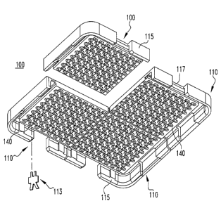
Fig. 3 is a top perspective view of an exemplary interface connector 100,
exploded, in accordance with the present invention, Fig. 4 is a side view of
the interface
connector of Fig. 3, and Fig. 5 is bottom perspective view of the exemplary
interface
connector of Fig. 3, assembled. The interface connector 100 may be similar to
the connector
described in International Publication number WO 98/15989 (International
Application
number PCT/US97/18066), and herein incorporated by reference. The connector
100 is a
modular array of a plurality of connectors 110 that are preferably non-
interlocking. The
individual connectors 110 can be directly neighboring each other so there are
no rows of
unused contacts between them on the underlying circuit board, as shown in
Figs. 3 and 5, or
they can be spaced apart so there are rows of unused contacts between them
(not shown).
2 0 The connector 110 typically has a plurality of apertures 140 through its
surface
for receiving contacts 113. The apertures 140 are typically disposed in an
array arrangement.
Furthermore, each connector 110 has a plurality of fusible elements 135, such
as solder balls,
disposed on a surface thereof, in an arrangement corresponding with the
apertures 140. As
shown in Fig. S, the solder balls 135 are partially disposed within associated
apertures 140 in
2 5 the connector housing 1 S0. The solder balls 135 are used for self
centering the connector 100
to an underlying substrate or printed circuit board. Each connector 110
preferably has a wall
115 around a portion of its periphery, so that when the modular connector 100
is fully
assembled, the walls 115 form an enclosure around the periphery of the
connector 100. The
walls 115 can have keying features 117 for mating with another connector.
3 0 Thus, the present invention solves a reliability failure mechanism, CTE
m~smatch, by partitioning an interface connector into multiple smaller modular
sections such
n
i
i
CA 02339498 2001-03-05
BERG2458/C2343 - ~ - PATENT
that each modular component is reliable and positioned together to form a
larger array.
Preferably, each component is de-coupled from the next and located through a
principle of
self centering of the BGA attachment to form a larger array.
The present invention provides a completed array by positioning the
components together so as not to interrupt any row or column (i.e., the
contacts maintain the
same pitch spacing) thus providing the most optimal electrical association
with an array
package or board array configuration. Unique array configurations can also be
constructed
such as depopulated areas such as peripheral array configurations, and
clustered arrays in the
form of small array groups located in close proximity to one another.
Fig. 6 is a top view of another exemplary interface connector 200 in
accordance
with the present invention. The connector 200 has a modular construction, but
there are no
contacts in a particular area (e.g., the center, as shown). More particularly,
the connector 200
comprises a plurality of connectors 210 that are preferably non-interlocking.
The individual
connectors 210 can be directly neighboring each other so there are no rows of
unused contacts
between them on the underlying circuit board, or they can be spaced apart so
there are rows
of unused contacts.between them, or even have empty space between them; as
shown. Each
connector 210 could include a perimeter wall or frame, such as wall 215 to
define the
perimeter of connector 200. Similar to the connectors described above, each
connector 210
has a plurality of fusible elements, such~as solder balls, disposed on a
surface, for mating to
2 0 an underlying substrate or circuit board.
Fig. 7 is a top view of a further exemplary interface connector 300 in
accordance with the present invention mounted on a substrate S, and Fig. 8 is
a top
perspective view of the connector 300 in a mated condition with a mating
connector 300',
which is preferably mounted on a substrate S'. The interface connectors may be
similar to the
connector described in U.S. Patent Application serial no. 09/209,132, pending,
and herein
incorporated by reference. The connector 300/300' has a modular construction
and comprises
a plurality of connectors 310/310' that are non-interlocking and. disposed in
a side by side
relationship. Similar to the connectors described above, each connector
310/310', has ~a
plurality of fusible elements 335/335', such as solder balls, disposed on a
surface, for mating
3 o to an underlying substrate or circuit board S/S'. The elements 335/335'
can be disposed
though apertures 340' in the housing of the connectors 310/310'. Although only
two
w
CA 02339498 2001-03-05
. ~ . ~ERG2458/C2343 - $ - . PATENT
connectors 310/310' are shown for each connector 300/300', it is contemplated
that any
number of connectors can be incorporated into the connector 300/300'.
In connector 300/300', there are no rows of unused contacts between the
connectors 310/310'. In another exemplary interface connector 400/400', as
shown in Fig. 9,
there is unused space 420 between the connectors 410/410'. The unused space
can receive one
or more frames 450. Frames 450 can be soldered to substrate S and can help
provide rigidity
to the substrate S, help control the effects of CTE and can include hinge
structure 460 to help
align and mate a pair of connectors.400,400'. Various projections on frame 460
engages
corresponding recesses in connectors 410/410' to seat connector 410/410'
within frame 460.
1 o The present invention addresses the effects of CTE mismatch by
modularizing
or splitting up the size of an array (e.g., connector 100) into smaller arrays
or components
(e.g., connectors 110) that have less differential displacements and therefore
improved
electrical performance and reliability.
The present invention addresses the issue of coplanarity and mold-ability (the
ability to repeatability manufacture a component using a molding process such'
as
thermoplastic molding) by modularizing or splitting up the size of an array
into smaller arrays
or components that can be produced flatter and easier through conventional
molding
processes.
Figure 10 shows an alternative embodiment of the present,rinvention. Similar
2 0 to connectors 410,410' and frames 450/450' of Figure 9, connector 500
mates with
corresponding connector 500'. Each connector includes a plurality of smaller
connector
modules 510'. Modules 510' house contacts (now shown) to which fusible
elements 535
secure. Fusible elements 535 preferably at least partially reside in recesses
540. A single
frame 550' can surround modules 510 and not extend between modules 510 at
unused space
2 5 520. As with the other embodiments, frame 550' could be any suitable
material such as metal
or plastic.
The problem with simultaneous parallel mating is the peak mating force is
experienced simultaneously as all the contacts engage instantaneously.
Connector mating
forces are comprised in two stages; one is the initial mating where the beams
deflect open and
3 0 the contacts, engage. This force is characterized by friction, contact
angles and the normal
forces of the engaging contacts. Stage two is characterized by .dynamic
sliding frictional
r
CA 02339498 2001-03-05
BERG2458/C2343 - 9 - PATENT
forces.
The present invention addresses the issue of high mating forces through an
angular mating concept or a pivoting mating concept such as that shown in
Figs. 7-10.
Features on the modular component or components assist in bringing the
components together
in an angular mating whereby the contacts are oriented to allow the plug
contact to transverse
into the receptacle contact without stubbing to engage each segment of
contacts sequentially
rather than simultaneously to reduce the peak insertion force by distributing
these individual
forces over a sequence of mating steps.
The modular components of the present invention canprovide overall mating
alignment of multiple components by providing features on certain components
that work
together or. function individually as features to provide the desired mating
alignment for
successful mating of the complete assembly.
This concept relies on an accurate positional relationship of the solder ball
and
the contact to maintain the mating conditions desirable for the individual
components to align
for successful mating. This is preferably achieved by the contact tip
protruding into a ball
cavity such that the solder will equally surround the contact tip to
facilitate this relationship.
Although the present invention has been described with respect to BGAs, other
packages, such as,uBGA and other chip scale grid array (CSGA) type packages,
flip chip, and
C4 type connections can also be used~with the present invention.
2 0 Although illustrated and described herein with reference to certain
specific
embodiments, the present invention is nevertheless not intended to be limited
to the details
shown. Rather, various modifications may be made in the details within the
scope and range
of equivalents of the claims and without departing from the invention.