Note: Descriptions are shown in the official language in which they were submitted.
CA 02339798 2001-02-06
WO 00/08764 -1- PCT/EP99/05005
DIGITAL RECEPTION WITH RADIO FREQUENCY SAMPLING
BACKGROUND
The present invention relates to analog-to-digital conversion, and more
particularly to analog-to-digital conversion of a signal at radio frequency
sampling
rates.
The role of telecommunications continues to grow in today's world. This is
true
not only in business settings (where communications are very often vital), but
also in
the day-to-day lives of individuals. With the advent of mobile communications
(e.g.,
cellular telephone systems), individuals with hectic lifestyles find that they
are more and
more dependent on their personal communication devices to keep in touch with
business
associates as well as with friends and family.
Because of this increased dependence, the drive to make mobile communication
devices more flexible and more reliable grows steadily. Research continues in
an effort
to reduce the size and power consumption of portable communications devices,
in order
to make them more convenient to carry while increasing their useful life
between
recharging.
In an effort to accomplish these goals, the trend has been to substitute
digital
technology for analog technology. In addition to achieving the goals of
reduced size
and power consumption, the substitution of digital technology for analog
technology has
resulted in increased quality of service because analog components are very
often
responsible for introducing problems like nonlinearities, distortions and
spurious
reception. Spurious reception is caused by mixing a higher harmonic of a
spurious
signal with a higher harmonic of the local oscillator, thereby generating a
signal close
to the intermediate frequency, fø:
.frF ~ I m ' fsr - n ' fio
SU6ST1TUTE SHEET (RULE 26j
CA 02339798 2001-02-06
W,O 00/08764 PCT/EP99/05005
a , , _2_
where jsp is the spurious signal's frequency, JLp is the local oscillator
frequency, and m
and n are the order of the signal and the local oscillator harmonic,
respectively.
Solving forJsp gives:
_ 1 n
JSP ~ ~ JI F +' - . JLO
m m
where the positive sign holds if the local oscillator frequency is above that
of the
wanted signal, and the negative sign occurs if it is below that of the wanted
signal.
Despite the desire to utilize digital technology as much as possible, state of
the
art receivers continue to include one or two analog Intermediate Frequency
(IF) stages
before the signal is sampled by a multi-bit analog-to-digital (A/D) converter.
The
reason for this is that radio frequencies intended to be used for mobile radio
applications are in the range of I or 2 gigahertz or above. Because
conventional multi-
bit A/D-converters are characterized by a limited input bandwidth, sampling at
the
radio frequency (RF) rate has not been possible. And, without A/D conversion,
analog
technology is the only means available for initially processing the received
RF signal.
S. Yang, et. al., "A tunable bandpass sigma-delta A/D conversion for mobile
communication receiver," 1994 IEEE 44th Vehicular Technology Conference, pp.
1346-1350, vol. 2 (1994) describes a receiver with one analog downconversion
and
techniques for tuning such a receiver by means of sigma-delta modulation.
The further prior art document US-5757867 discloses an analog-to-digital
converter in
which a decimation filter is connected to the output Y of a sigma-delta
modulator. The
decimation filter transforms the low resolution data stream into a high
resolution data
stream at a lower rate. It includes a digital mixer and lowpass downsampling
filters to
operate on the digital output Y.
In another prior art document US-5621345 a circuit that includes an
oversampling ADC
is disclosed that receives the input waveform and converts it to digital
samples at an
oversampling rate; a first digital filter which receives the digital samples
from the ADC
directly and provides the inphase component samples of the input waveform; and
a
second digital filter which receives the digital samples from the ADC directly
and
provides the quadrature component samples of the input waveform.
AMENDED SHEET
SUBSTITUTE SHEET (RULE 26)
CA 02339798 2001-02-06
-2a-
SUMMARY
It is therefore an object of the present invention to provide improved methods
and apparatuses for reception of radio frequency signals.
In accordance with one aspect of the present invention, the foregoing and
other
objects are achieved in a radio receiver that receives a radio frequency
signal, and uses
sigma-delta analog-to-digital conversion techniques that sample the radio
frequency
signal at a sampling rate and generates therefrom 1-bit digital samples
representing an '
1o intermediate frequency signal. Whether or not the sampling rate is at,
above or below
the Nyquist rate of the radio frequency signal, the sampling rate is
preferably many '
times higher than the signal bandwidth. Having generated the intermediate
frequency
signal, demodulation is then used to generate in-phase and quadrature samples
from the
P09539-DBO PCT/EP/05005 O 1 / 10/01
AMENDED SHEET
CA 02339798 2001-02-06
WO 00/08764 -3- PCT/EP99/05005
intermediate frequency signal. An advantage of this technique is that
demodulation may
be performed in a purely digital manner.
In another aspect of the invention, the intermediate frequency is a difference
between the radio frequency and a closest harmonic of the sampling rate.
In some embodiments, demodulation comprises generating a first mixed signal
by combining the 1-bit digital samples representing the intermediate frequency
signal
with a first sequence representing a cosine mixing signal; and generating a
second
mixed signal by combining the 1-bit digital samples representing the
intermediate
frequency signal with a second sequence representing a sine mixing signal. The
first
and second mixed signals are then decimated to generate the in-phase and
quadrature
samples. In these embodiments, the intermediate frequency may be one fourth of
the
sampling rate.
In yet another aspect of the invention, exclusive-OR logic gates may be used
to
generate the first and second mixed signals.
In still another aspect of the invention, demodulation may alternatively be
performed by receiving the 1-bit digital samples representing the intermediate
frequency
signal and generating therefrom first and second decimated signals, wherein:
the first
decimated signal is based on the 1-bit digital samples; the second decimated
signal is
based on a time-shifted version of the 1-bit digital samples; each of the
first and second
decimated signals has one sample for every number, N, of I-bit digital samples
representing the intermediate frequency; and the time-shifted version of the I-
bit digital
samples is the I-bit digital samples delayed by an amount, ~n cycles of the
sampling
rate. On may represent an odd multiple of a quarter period of the intermediate
frequency. The first and second decimated signals are then bandpass filtered
to
generate the respective in-phase and quadrature samples.
In yet another aspect of the invention, demodulation may alternatively be
performed by considering the intermediate frequency to be a first intermediate
frequency, and bandpass filtering and decimating the intermediate frequency
signal to
generate a digital signal having a second intermediate frequency. A
demodulator is then
used for reconstructing the in-phase and quadrature samples from the digital
signal
having the second intermediate frequency. In these embodiments, the bandpass
filtering
has a bandpass characteristic around the first intermediate frequency.
SUBSTITUTE SHEET (RULE 26)
CA 02339798 2001-02-06
WO 00/08764 PCT/EP99/05005
BRIEF DESCRIPTION OF THE DRAWINGS
The objects and advantages of the invention will be understood by reading the
following detailed description in conjunction with the drawings in which:
FIG. I a is a block diagram of a sigma-delta-modulator A/D converter, and FIG
lb is an equivalent model of the same converter;
FIG. 2 is a block diagram of a digital receiver structure based on radio
frequency sampling by means of a sigma-delta modulator A/D converter in
accordance
with one aspect of the invention;
FIG. 3 is a graph of the spectra of signal and quantization noise after
sampling;
FIGS. 4a and 4b depict alternative embodiments of a digital receiver structure
with direct conversion to I and Q by digitally sub-sampling two time-shifted
sequences
from the sigma-delta-modulator with bandpass decimation filters, in accordance
with
one aspect of the invention;
FIG. 5 is a block diagram of a digital double superheterodyne receiver
structure
IS having two intermediate frequencies in the digital domain in accordance
with another
aspect of the invention;
FIG. 6 shows an exemplary hardware implementation of a fast sigma-delta-
modulator A/D converter that is suitable for use with the receivers, in
accordance with
another aspect of the invention; and
FIG. 7 is a block diagram of an alternative embodiment of a digital receiver
structure based on radio frequency sampling by means of a sigma-delta
modulator A/D
converter in accordance with one aspect of the invention.
DETAILED DESCRIPTION
The various features of the invention will now be described with respect to
the
figures, in which like parts are identified with the same reference
characters.
Radio frequency sampling in the gigahertz range is feasible with one-bit A/D
converters that can be built with commercially available high speed logic
components.
Such sampling enables the analog circuitry of conventional receivers to be
replaced by
digital circuitry, thereby obtaining the various benefits described in the
BACKGROUND section above. A one-bit A/D converter will exhibit very high
SUBST11TUTE SHEET (RULE 26)
CA 02339798 2001-02-06
WO 00/08764 PCT/EP99/05005
quant~zation noise, however. One technique for reducing this is by digital low
pass
filtering and decimation, a strategy that exchanges resolution for sample
rate.
As an alternative, the noise performance can be considerably improved by
highly oversampling the signal modulated on the RF signal, and then employing
a
sigma-delta-modulator for noise shaping in order to achieve the required
dynamic range
for the digitized signal. FIG. 1 a shows a block diagram of a sigma-delta-
modulator
A/D converter, and FIG. 1 b shows an equivalent model of the same converter.
Looking first at FIG. la, an A/D converter 101 is provided to generate a
digital signal
that is intended to represent an analog input signal, X. In order to reduce
the
quantization noise in the range of the signal spectrum associated with the
digitization
process, the output of the A/D converter 101 is supplied to a feedback path,
where it is
first converted back into an analog signal by means of a D/A converter 103.
The
resultant analog feedback signal is subtracted from the analog signal 107 that
feeds the
A/D converter 101. The resultant difference signal is applied to a filter 105
whose
output is combined with the input analog signal, X. This combined signal 107
is the
analog signal that is supplied to the A/D converter IOI.
A better understanding of this process will be gained by referring now to FIG.
1 b. In this model of the sigma-delta-modulator A/D converter, the A/D and D/A
converters 101 and 103 are replaced by a summing junction 109 that adds a
signal
representing the quantization noise, Q. Given the analog input signal X, the
quantization noise Q, the analog representation, Y, of the output and the
digital output
signal Y, the transfer function of the sigma-delta-modulator A/D converter is:
Y=X+~1-H)Q
With a suitable filter characteristic, H, in the feedback loop of the sigma-
delta-
modulator, the quantization noise spectrum can be shaped such that it is
suppressed as
much as possible at frequencies occupied by the signal spectrum. Techniques
for
determining the filter characteristic are known, and usually start with a
linear approach
by setting the noise transfer function I-H(c~) to some known filter
characteristic with a
SUBSTITUTE SHEET (RULE 26)
CA 02339798 2001-02-06
WO 00/08764 PCT/EP99/05005
-6
high attenuation in the range of the signal spectrum, such as a bandstop
Butterworth,
Chebychev or Cauer characteristic. The zeros and poles of H(w) can then be
derived
from this. Since a sigma-delta modulator is a nonlinear device, H(w) derived
by the
linear method is an approximation and should be further optimized by
experiments or , .
simulations in the time domain. This is common practice today, since no direct
analytical approach is known. Having derived the suitable filter
characteristic for the
sigma-delta modulator, preferred implementations may utilize passive filters,
such as
LC or microstrip filters, because of the required high frequency operation.
The corresponding dynamic range increases with the over-sampling ratio (i.e.,
sample rate divided by twice the signal bandwidth) and the order of the sigma-
delta-
modulator, which is related to the filter order. For example, a sigma-delta-
modulator
of fifth order and an over-sampling ratio of 32 results in a 90 dB dynamic
range,
corresponding to 15 bits. The relationship between the dynamic range, over-
sampling
ratio and the order of the sigma-delta-modulator is described, for example, in
Richard
Schreier, "An empirical study of high-order single-bit delta-sigma
modulators", IEEE
TRANSACTIONS ON CIRCUTTS AND SYSTEMS -II: ANALOG AND DIGTTAL
SIGNAL PROCESSING, vol. 40, No. 8, August 1993, p. 465.
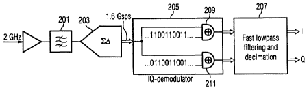
FIG. 2 shows a block diagram of a first digital receiver structure based on
radio
frequency sampling by means of a sigma-delta modulator A/D converter as
described
above. A radio frequency signal (e.g., a 2GHz signal) is received and
processed by an
anti-aliasing filter 201. The filtered signal is then supplied to a one-bit
sigma-delta
modulator A1D converter 203. The digital output from the one-bit sigma-delta
modulator A/D converter 203 is then further processed by an IQ-demodulator 205
and a
fast lowpass/decimation filter 207.
In operation, the one-bit sigma-delta-A/D converter 203 may sub-sample the
filtered radio frequency signal (i.e., the filtered radio frequency signal is
sampled at
less than the Nyquist rate for the radio frequency signal, which would be two
times the
radio frequency), thus converting the signal to an intermediate frequency in
the digital '
domain that is the difference between the radio frequency and the harmonic of
the
sample frequency closest to it. Note that the signal modulated on the radio
frequency
carrier is band-limited, so that even though the radio frequency signal is sub-
sampled,
the modulating signal is still highly oversampled. For example, given a 5 MHZ
signal
SUBSTITUTE SHEET (RULE 26)
CA 02339798 2001-02-06
Wp 00/08764 PCT/EP99/05005
_7
modulated on a 2 GHz radio frequency carrier, a sampling rate close to the
radio
frequency would highly oversample the modulating signal even though the radio
frequency carrier would be sub-sampled, Of course, sub-sampling of the radio
frequency signal is not a requirement. In alternative embodiments, the radio
carrier
may be sampled above its Nyquist rate, thereby giving even more oversampling
of the
modulating signal.
Returning now to a discussion of those embodiments in which sub-sampling of
the radio frequency carrier is utilized, since the sub-sampled signal is at a
non-zero
intermediate frequency, a so-called bandpass sigma-delta-modulator is
preferably used
as part of the one-bit sigma-delta-A/D converter 203. Bandpass sigma-delta-
modulators
are well-known in the art, and need not be described here in greater detail.
The anti-
aliasing filter 201 and the IQ-demodulator 205 become most simple when the
sampling
rate, FS, is chosen to be four times the digital intermediate frequency, F~
(i.e., F~ _
FS/4). In this case, the cosine and sine mixing signals are represented by the
respective
sequences . . . I-1-111-I-11. . . and . . . 11-1-111-1-1 . . . which, in
digital form,
correspond to the respective sequences . . . 10011001 . . . and . . . l
1001100 . . . . It
can be seen that, although the two sequences have the same form (i.e., two
bits of "1"
followed by two bits of "-1 "), the sequence for the cosine mixing signal
leads the
sequence for the sine mixing signal by one bit. Together with the one-bit
signal from
the sigma-delta-A/D converter 203, the multiplication operations in the IQ-
demodulator
reduce to selectively inverting or not inverting the corresponding signal
bits, such as by
means of the illustrated logical exclusive-or ("XOR") operations 209, 211.
Two cases have to be distinguished for the digital intermediate frequency. The
first is the case in which the m-th harmonic of fs closest to the radio
frequency, f~, is
below f~. The second is the case in which the m-th harmonic of fs closest to
the radio
frequency, fRg, is above f~. For case l
_ 1
m~S ~ ~RF ~ f!F I,øm + 1 ' RFI
and for case 2:
SUBSTITUTE SHEET (RULE 26)
CA 02339798 2001-02-06
W!J 00/08764 PCT/EP99/05005
-g
1
refs > .fief ~ frF =I4m - I fRF
For example, for the first case with fR~2 GHz and m=1 the intermediate
frequency is 400 MHZ and the sample rate fs=4fIF=1.6 giga-samples per second
(lisps). With that sample rate, a 20 MHZ wide signal is oversampled with an '
oversampling ratio of 40.
FIG. 3 shows the spectra of signal and quantization noise after sampling. The
bandpass sigma-delta-modulator within the one-bit sigma-delta A/D converter
203
suppresses the quantization noise at the signal frequencies. This makes it
possible for
the quantization noise to be removed by the lowpass/decimation filter 207
without
affecting the signal. Since the harmonics of the signal spectrum are far
apart, the
IO characteristic 301 of the analog anti-aliasing filter 201 is rather flat,
which is a
relatively easy requirement to satisfy.
Principally, then, FIG. 3 illustrates what frequencies can pass through the
analog anti-aliasing filter in the front end. The signal with bandwidth B
modulated on
the radio carrier f~ is converted to the intermediate frequency f~ by the sub-
sampling
IS operation. However, all frequencies received within the signal bandwidth
located at the
harmonics of the radio carrier plus/minus the intermediate frequency nfRF~fø,
where
n=2, 3, ..., are also converted into the wanted signal bandwidth at fø. All of
these
spectral locations have to be filtered out. Consequently, the anti-aliasing
filter at the
front-end has to pass the signal spectrum at f~ undisturbed and stop all
frequencies
20 below the upper limit of the next "alias band" below (e.g., fs-f~+B/2 for
the example
shown in FIG. 3) and above the lower limit of the next "alias band" above
(e.g.,
2fg-f~-B/2 for the example shown in FIG. 3). This is the equivalent of an
image
suppression filter found in analog mixer stages of conventional receivers.
In accordance with one aspect of the invention, the mufti-bit representation
of
25 the analog input signal is obtained, in part, by means of the
lowpass/decimation filter
207 that suppresses the shaped noise without affecting the signal. Such a
decimation
filter faces the problem of high speed. Because of these high demands,
preferred
embodiments of the invention utilize decimation filter techniques as described
in U.S.
SUBSTITUTE SHEET (RULE 26)
CA 02339798 2001-02-06
W,O 00/08764 PCT/EP99/05005
-9
Patent Application No. (Attorney Docket No. 027559-012), filed in the
name of Dietmar Lipka, entitled "Multiplierless Digital Filtering", which is
hereby
incorporated herein by reference in its entirety.
A second digital receiver structure with direct conversion to I and Q by
digitally
sub-sampling two time-shifted sequences from the sigma-delta-modulator with
bandpass
decimation filters is shown in FIGS. 4a and 4b. These embodiments differ from
the one
shown in FIG. 2 in that the digital intermediate frequency need not be
restricted to the
case in which f1F = fs/4.
Assume first that the relationship between the intermediate frequency and the
sampling rate is arbitrary: fIp=fs/x. Direct conversion to either the I or Q
signal is
obtained by sub-sampling, that is, decimating, the signal in the digital
domain with a
sub-multiple of fIp given as fD=fIF/k=fg/(kx), where fD is the sub-sampling
rate in the
digital domain and k= 1,2,3, . . . . The I and Q components can be separated
by
generating two sub-sampled sequences that are mutually time shifted with
respect to one
IS another by an odd numbered multiple of one fourth of an intermediate
frequency period
T~ 1/f~: i=(2l+1 ) T~/4, l=0, 1, 2,... . It then follows that the two
sequences
have to be shifted by an amount Vin= T/TS=(21+1 )x/4 sample points with
respect to
one another, where Tg=1/fs. Since On has to be an integer value, x is
restricted to
being a multiple of 4, expressed here as x=4~t, lt=1, 2, 3, . . . . With that,
the possible
intermediate frequencies for case 1 identified above are:
1
mfs ~ fRF ~ .fiF = 4m~1 + l fx~
and for case 2, the possible intermediate frequencies are:
1
mfs ~ fRf ~ .f~F = 4mu -1 'fRF
If the intermediate frequency is determined with these formulas, the sampling
rate of the sigma-delta-modulator is calculated by fs=4Nfø and the number of
one-bit
sample cycles between the decimated I and Q signal data points is calculated
by
On=(2l+1 )p.
SUBSTITUTE SHEET (RULE 26)
CA 02339798 2001-02-06
WQ 00/08764 PCT/EP99/05005
- I 0
The combined bandpass decimation filtering and IQ-demodulation is
implemented utilizing decimation filter techniques described in the above-
mentioned
U.S. Patent Application No. (Attorney Docket No. 027559-012), entitled
"Multiplierless Digital Filtering", which is incorporated herein by reference
in its ,
entirety. Generally, decimation by N in this filter may be accomplished with a
shift
register that reads the one-bit samples from the sigma-delta-modulator. Each
time a
number of N 1-bit input data samples has been (sequentially) loaded into the
shift
register, a block of data samples is clocked into a latch. The latched bits
are then fed
into a filter structure running at the decimated clock rate. The filter
structure may
comprise, for example, a memory or a cascade of memories whose outputs are
added,
yielding the filtered signal. The memories contain additive combinations of
the filter
coefficients. Where the filter order, L, is larger than the number of latched
bits
supplied to the filter structure (i.e., is larger than the size of a presently
received
decimated data signal), the filter structure may include one or more cascade-
connected
latches for storing earlier-received decimated data signals. A number of
alternative
embodiments of the decimation filter techniques are described in the above-
mentioned
"Multiplierless Digital Filtering" patent application, any one of which could
easily be
adapted for use in conjunction with the techniques described here.
Utilizing these principles, the two mutually time-shifted sequences can be
obtained by several alternative methods. In one embodiment, as illustrated in
FIG. 4a,
a sigma-delta A/D converter 401 supplies its 1-bit output to an N-bit shift
register 403,
which clocks in the bits at the fast sampling clock rate, fs. First and second
latches,
405 and 407, are each coupled to receive N-bit wide data from the N-bit shift
register
403. The first and second latches 405 and 407 are clocked by means of
respective ones
of two phases of the decimated clock. The offset between the two phases of the
decimated clock is ~n cycles of the fast sampling clock fs. In alternative
embodiments,
the N-bit shift register 403 and first and second latches 405 and 407 may be
expanded
to a length of L, in order to effect higher-order filtering without affecting
the amount of
decimation.
Focusing again on the embodiment-illustrated in FIG. 4a, the first and second
'
latches 405 and 407 supply their outputs to respective ones of first and
second cascaded
bandpass filter structures 409, 41 1. The output of the first cascaded
bandpass filter
SUBSTIfTUTE SHEET (RULE 26)
CA 02339798 2001-02-06
VlJO 00/08764 PCT/EP99/05005
-11
structure 409 is the in-phase signal, I, and the output of the second cascaded
bandpass
filter structure 41 1 is the quadrature signal, Q. Each of the cascaded
bandpass filter
structures 409, 411 may include a memory or a cascade of memories whose
outputs are
combined (e.g., added), yielding the filtered signal. The memory or memories
contain
additive combinations of the filter coefficients. For a filter of order L,
with LAN, the
first and second cascaded bandpass filter structures 409, 41 1 may include
cascade-
connected latches for storing earlier received bits. The outputs from the
cascade-
connected latches are, in this case, supplied for use in addressing the one or
more
memories.
In an alternative embodiment, as shown in FIG. 4b, one latch 417 is utilized
rather than the two latches 405, 407. In this case, the shift register 415 and
the latch
417 are each N+ ~n bits wide. In the illustrated embodiment, 0n=2, but of
course this
need not be the case for all embodiments. The first N bits (i.e., bits 1 . . .
N) are
supplied to a first cascaded bandpass filter structure 409, and the last N
bits (i.e, bits
On+1 ... N+ On) are supplied to a second cascaded bandpass filter structure
411.
These two groups of bits are processed synchronously by the two cascaded
bandpass
filter structures 409, 411. The latch 417 and the first and second cascaded
bandpass
filter structures 409, 411 are each clocked with a decimated version (i.e.,
decimation
ratio of 1:N) of the fast sampling clock, fs.
The techniques illustrated in FIG. 4b may be applied to filters of order L.
One
possibility is for the shift register 415 and the latch 417 to each be L+ pn
bits wide and
with the decimated clock still specified to occur once for every N assertions
of the fast
sampling clock rate. Other possibilities include the use of the illustrated N+
On-bit
wide shift register 415 and latch 417 in conjunction with cascade-connected
latches (not
shown) located within each of the first and second filter structures 409, 411.
Each of
the cascade-connected latches would store earlier-received data bits (clocked
at the
decimated clock rate), and would supply these stored bits (at the decimated
clock rate)
to an address input port of a memory device, as explained more fully in the
above-
identified "Multiplierless Digital Filtering" patent application.
For each of the embodiments illustrated in FIGS. 4a and 4b, the filters 409,
411
have to be designed as bandpass filters for the signals at the intermediate
frequency in
order to remove the quantization noise around it. The cascaded bandpass
filters 409,
SUBSTITUTE SHEET (RULE 26j
CA 02339798 2001-02-06
WHO 00/08764 PCf/EP99/05005
-12
41 1 deliver the respective I and Q signals at the decimated rate. The fact
that the I and
Q signals belong to different time instants must be considered. For high
decimation
factors, this timing error can be neglected. Otherwise, proper time alignment
can be
achieved with a subsequent interpolator.
In yet another aspect of the invention, a third digital receiver structure is
shown
in FIG. 5. The structure has two intermediate frequencies in the digital
domain and can
thus be regarded as a digital double superheterodyne. The signal is converted
to the
first intermediate frequency by the sampling performed by the sigma-delta A1D
converter 501. The second intermediate frequency, IF2, results from the
decimation
process in the decimation filter 503. Let D be the decimation factor of the
digital
bandpass decimation filter, where D is an integer number, fs/D is the
decimated
sampling rate and k~fs/D is the k-th harmonic of the decimated sampling rate,
where
k=1,2,... . Then IF2 is the difference between IFI and the nearest harmonic
k~fs/D.
In practice, fRF is given and D and fs have to be chosen appropriately. D and
fg have
to be arranged to obtain a value of IF2 such that demodulation of I- and Q-
signals is
possible. Furthermore, it is advantageous if IF1 is as close as possible to
fs/4, in other
words, to relax the requirements for the anti-aliasing filter. (In this case
the alias
frequencies where unwanted signals are converted to IF1 (spurious reception)
are more
equidistantly located on the frequency axis, that is with maximum distance
with respect
to each other as illustrated in FIG. 3). The decimation filter 503 has a
bandpass
characteristic around IF1. A digital IQ-demodulator 507 receives the output
from the
bandpass and decimation filter 503, and reconstructs the I and Q signals from
the
second digital IF signal. In general, this IQ-demodulator 507 performs full
multiplications, but can be simplified if IF2 is one fourth of the decimated
sampling
frequency.
The clock rate of the sigma-delta-A/D converter is in the gigahertz range for
all
receiver structures described above. In accordance with another aspect of the
invention, FIG. 6 shows an exemplary hardware implementation of a fast sigma-
delta- ;
modulator A/D converter that is suitable for use with these receivers. The one-
bit A/D
converter portion can be realized with a decision device 601 having an output
coupled
to the data input port of a flip-flop 603. The flip-flop 603 is clocked at the
fast
SUBSTITUTE SHEET (RULE 26)
CA 02339798 2001-02-06
WO 00/08764 PCT/EP99/05005
-13-
sampling rate, fs. The output from the flip flop 603 supplies the 1-bit
digital output
signal from the sigma-delta A/D converter.
In a first feedback path, a level shifter 605 is provided for use as a one-bit
D/A
converter. The level shifter 605 is coupled to receive the 1-bit digital
output signal
from the flip-flop 603. The upper and lower output voltage of the level
shifter 605
determines the input voltage range of the sigma-delta-A/D converter.
Consequently, if
the level shifter 605 is adjustable, it can be used for gain control.
The analog part consists of couplers and one or more filters. A first coupler
607
combines the analog output from the level shifter 605 with a second analog
signal that is
derived from the analog signal that is supplied to the input of the decision
device 601.
An optional first filter 615 having a transfer function G(w) may be included
to process
the second analog signal prior to its being supplied to the coupler 607.
The output of the first coupler 607 is supplied to a second filter 609, that
is also
in the feedback path. This second filter 609 may be realized with a micro-
strip filter.
In alternative embodiments, SAW, resonator or even LC filters may be used
instead.
A second coupler 61 I is provided in the forward path of the sigma-delta A/D
converter. The second coupler 611 combines the analog RF input signal with the
analog signal supplied at the output of the second filter 609. The output
signal of the
second coupler 611 may be supplied to the input port of the decision device
601.
In an alternative embodiment, a third filter 613 is also provided in the
forward
branch, between the second coupler 611 and the decision device 601. Where
H1(w) is
the filter characteristic of the second filter 609, H2(c~u) is the filter
characteristic of the
third filter 613, and G(t~) is the filter characteristic of the first filter
61 S, the transfer
function of the sigma-delta A/D converter is:
_ HZ I - H,HZG
I+H,HZ(1-G)X +I+H,H2(I-G)~
The above-described receiver structures are advantageous in that they greatly
reduce the amount of required analog circuitry, compared to conventional
designs.
This avoids, to a great extent, problems like nonlinearities and distortions
because no
mixers and intermediate frequency amplifiers are needed. Due to the inherent
linearity
SUBSTITUTE SHEET (RULE 26)
CA 02339798 2001-02-06
VSO 00/08764 PCT/EP99/05005
-14
of the sigma-delta-A/D converter, spurious reception is nonexistent. The high
sampling rate is beneficial because it imposes the least requirements on the
anti-aliasing
filter. Due to their essentially digital function, these receivers are highly
integratable,
thus having the potential for smallest size, lowest power consumption and high
reliability. Furthermore, they can be flexibly adapted to all standards by
simply
changing digital signal processing. In addition, an automatic gain control can
be
provided that requires simple circuitry because the level shifter 605 in the
feedback loop
need switch only between two voltage levels. Due to the low number of required
components, this type of receiver is also a low cost solution.
The various receivers described herein can each be used as a wideband
receiver,
such as for Wideband Code Division Multiple Access (W-CDMA). They may also be
used for all narrow band standards in mobile communication.
The invention has been described with reference to a particular embodiment.
However, it will be readily apparent to those skilled in the art that it is
possible to
embody the invention in specific forms other than those of the preferred
embodiment
described above. This may be done without departing from the spirit of the
invention.
For example, FIG. 7 is a block diagram of yet another receiver structure in
accordance with an aspect of the invention. As with the receiver depicted in
FIG. 2, a
radio frequency signal (e.g., a 2GHz signal) is received and processed by an
anti-
aliasing filter 701. The filtered signal is then supplied to a one-bit sigma-
delta
modulator A/D converter 703. The digital output from the one-bit sigma-delta
modulator A/D converter 703 is then further processed by an IQ-demodulator
705.
However, in place of the digital decimation filter of FIG. 2, the in-phase (I)
and
quadrature (Q) outputs from the IQ-demodulator 705 are supplied to respective
ones of
first and second analog lowpass filters 707. The I-bit data streams from the
IQ-
demodulator 705 can either be regarded as digital or (if the waveform of the
output gate
is taken into account) as analog. These signals are composed of the respective
baseband
I and Q signals and quantization noise. Thus, as an alternative to a digital
decimation
filter, the quantization noise in the I and Q signals can also be suppressed
by respective
ones of the first and second analog filters 707. The output signals from the
first and
second filters 707 have only the bandwidth of the baseband I and Q signals and
can be
sampled at a low rate with conventional first and second analog-to-digital
converters
SU9STITUTE SHEET (RULE 26j
CA 02339798 2001-02-06
WO 00/08764
PCT/EP99/05005
-15-
709. The combination of the sigma-delta-A/D converter with the 1-bit IQ-
demodulator
705 can be regarded as linear direct conversion. A drawback with respect to
the digital
decimation filter is that the I and Q signals have an offset. This offset,
however, can be
removed by means of digital signal processing.
Thus, the preferred embodiment is merely illustrative and should not be
considered restrictive in any way. The scope of the invention is given by the
appended
claims, rather than the preceding description, and all variations and
equivalents which
fall within the range of the claims are intended to be embraced therein.
SUBSTITUTE SHEET (RULE 26)