Language selection

Search

Patent 2340059 Summary

Third-party information liability

Some of the information on this Web page has been provided by external sources. The Government of Canada is not responsible for the accuracy, reliability or currency of the information supplied by external sources. Users wishing to rely upon this information should consult directly with the source of the information. Content provided by external sources is not subject to official languages, privacy and accessibility requirements.

Claims and Abstract availability

Any discrepancies in the text and image of the Claims and Abstract are due to differing posting times. Text of the Claims and Abstract are posted:

  • At the time the application is open to public inspection;
  • At the time of issue of the patent (grant).
(12) Patent: (11) CA 2340059
(54) English Title: MICROMECHANICAL SENSOR AND METHOD FOR PRODUCING SAME
(54) French Title: CAPTEUR MICROMECANIQUE ET SON PROCEDE DE PRODUCTION
Status: Deemed expired
Bibliographic Data
(51) International Patent Classification (IPC):
  • B81B 3/00 (2006.01)
  • B81C 1/00 (2006.01)
  • H04R 19/00 (2006.01)
  • H04R 19/04 (2006.01)
  • H04R 31/00 (2006.01)
(72) Inventors :
  • AIGNER, ROBERT (Germany)
  • BEVER, THOMAS (Germany)
  • TIMME, HANS-JORG (Germany)
(73) Owners :
  • INFINEON TECHNOLOGIES AG (Germany)
(71) Applicants :
  • INFINEON TECHNOLOGIES AG (Germany)
(74) Agent: FETHERSTONHAUGH & CO.
(74) Associate agent:
(45) Issued: 2003-12-23
(86) PCT Filing Date: 1999-08-03
(87) Open to Public Inspection: 2000-02-24
Examination requested: 2001-02-09
Availability of licence: N/A
(25) Language of filing: English

Patent Cooperation Treaty (PCT): Yes
(86) PCT Filing Number: PCT/DE1999/002375
(87) International Publication Number: WO2000/009440
(85) National Entry: 2001-02-09

(30) Application Priority Data:
Application No. Country/Territory Date
198 36 342.7 Germany 1998-08-11

Abstracts

English Abstract


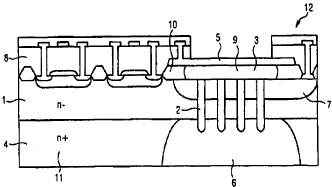
The invention relates to a micromechanical sensor and to a corresponding
production method, comprising the following steps: a) preparing a doped
semiconductor wafer (4); b) applying an epitaxial layer (1) that is doped in
such a way that a jump in the charge carrier density in the interface (11)
between the semiconductor wafer and the epitaxial layer occurs; c) optionally
etching ventilation holes (2) traversing the epitaxial layer and optionally
filling the ventilation holes with a sacrificial material; d) depositing at
least one sacrificial layer (9), at least one spacing layer (10), a membrane
(5) and optionally a semiconductor circuit (8) on the top side of the
epitaxial layer using a technology known per se, wherein the semiconductor
circuit may be applied after the membrane is formed or while depositing the
layers required to form the membrane; e) etching a hole (6) on the back part
of the sensor, wherein the etching method is selected in such a way that
etching advances in the direction of the top side and ceases in the interface
between the wafer (4) and the epitaxial layer (1) by changing charge carrier
concentration. The invention also relates to the utilization of the
micromechanical sensor in pressure sensors or microphones.


French Abstract

L'invention concerne un capteur micromécanique et son procédé deproduction, lequel comprend les étapes suivantes: a) préparationd'une tranche de semi-conducteur (4) dopée; b) application d'unecouche épithaxiale (1) qui est dopée de façon telle qu'à l'interface (11) entre la tranche de semi-conducteur et la couche épitaxiale se présente une discontinuité dans la densité des porteurs de charge; c) éventuellement, création par attaque d'ouvertures deventilation (2) qui traversent la couche épitaxiale et, éventuellement, remplissage des ouvertures de ventilation avec un matériau sacrificiel; d) application d'au moins une couche sacrificielle (9), d'au moins une couche d'espacement (10), d'une membrane (5) et, éventuellement, d'un circuit à semi-conducteur (8), selon une technologie connue en soi, sur la face supérieure de la couche épitaxiale, le circuit à semi-conducteur pouvant être appliquéaprès formation de la membrane ou pendant l'application des couches nécessaires à la formation de la membrane; e) création par attaque d'une ouverture (6) sur la face arrière du capteur, le procédé d'attaque étant choisi de façon telle que le processus d'attaque se produise en direction de la face supérieure et s'arrête à l'interface entre la tranche (4) et la couche épithaxiale (1) parmodification de la concentration des porteurs de charge. L'invention concerne également l'utilisation du capteur micromécanique dans des capteurs de pression ou dans des microphones.

Claims

Note: Claims are shown in the official language in which they were submitted.


6

CLAIMS:

1. A method of producing a micromechanical sensor,
which comprises:
providing a doped semiconductor wafer;
applying an epitaxial layer on the wafer and
ensuring that at least a portion of a region of the
epitaxial layer that faces the wafer is doped such that a
jump in a charge carrier density occurs at an interface
between the wafer and the epitaxial layer;
etching ventilation openings through the epitaxial
layer;
applying at least one sacrificial layer, at least
one spacer layer, and a membrane on the epitaxial layer;
etching an opening in a rear of the wafer using an
etching method such that the etching progresses towards a
top of the wafer and stops at an interface between the wafer
and the epitaxial layer by a changed charge carrier
concentration; and
removing the at least one sacrificial layer with
an etchant to expose the ventilation openings and to form a
membrane, a counterelectrode disposed underneath the
membrane, and a cavity disposed between the membrane and the
counterelectrode, the ventilation openings connecting the
cavity to the opening in the rear of the wafer.
2. The method according to claim 1, which comprises
using an electrochemical etching process to perform the step
of etching the opening in the rear of the water.


7


3. The method according to claim 2, which comprises
performing the step of etching the opening in the rear of
the wafer in two steps:
first, performing a step of wet chemically etching
for a defined time period until the etching is close to the
interface between the wafer and epitaxial layer; and
second, performing a step of electrochemically
etching, the electrochemically etching being stopped by the
changed charge carrier concentration between the wafer and
the epitaxial layer.
4. The method according to claim 1, which comprises
performing the step of etching the opening in the rear of
the wafer in two steps:
first, performing a step of wet chemically etching
for a defined time period until the etching is close to the
interface between the wafer and epitaxial layer; and
second, performing a step of electrochemically
etching, the electrochemically etching being stopped by the
changed charge carrier concentration between the wafer and
the epitaxial layer.
5. The method according to claim 1, which comprises
filling the ventilation openings with a sacrificial
material.
6. The method according to claim 1, which comprises
applying a semiconductor circuit on the epitaxial layer
after formation of the membrane.
7. The method according to claim 1, which comprises
applying a semiconductor circuit on the epitaxial layer
during application of layers needed to form the membrane.


8

8. A micromechanical sensor, comprising:
a substrate having a surface and formed from a
doped semiconductor material;
an epitaxially grown layer projecting over the
entire surface of said substrate;
a membrane configured on top of said epitaxial
layer and made predominantly from a material selected from
the group consisting of polycrystalline silicon and
monocrystalline silicon;
a counterelectrode disposed underneath said
membrane;
a rear opening formed in said substrate; and
a cavity formed between said membrane and said
counterelectrode;
said epitaxial layer having an area that faces
said substrate with at least a portion thereof that is doped
such that a jump in a charge carrier concentration occurs at
an interface between the substrate and the epitaxial layer.
9. The micromechanical sensor according to claim 8,
wherein said substrate is made from silicon with a charge
carrier concentration of more than 10 18 cm-3.
10. The micromechanical sensor according to claim 8,
wherein said portion of said area of said epitaxial layer
that faces said substrate has a charge carrier concentration
of less than 5 × 10 14 cm-3.
11. The micromechanical sensor according to claim 8,
comprising a semiconductor circuit, said epitaxial layer


9
having a top with said semiconductor circuit applied
thereto.
12. The micromechanical sensor according to claim 8,
wherein said counterelectrode is formed with ventilation
openings connecting said cavity with said rear opening.
13. Use of the micromechanical sensor according to
claim 8 for pressure sensors or microphones.

Description

Note: Descriptions are shown in the official language in which they were submitted.


CA 02340059 2001-02-09
Description
Micromechanical Sensor and Method for Producing Same
The invention concerns a micromechanical sensor comprising a
substrate, an epitaxial layer projecting over the entire substrate
surface, a membrane, a counterelectrode, a hole on the back and a
hollow space which is situated between membrane and
counterelectrode. Furthermore, a method for the production of the
aforementioned micromechanical sensor is described.
Micromechanical sensors are described in a number of documents.
Thus, for example, the document US 5, 110, 373 describes a method for
the production of a silicon membrane which is used in
micromechanical sensors. The document JP 63084072 shows a pressure
sensor as well as a method for producing same.
In applications where low costs and space requirement are of
importance such as, for example, pressure sensors, microphones or
acceleration sensors, miniaturized micromechanical sensors having
semiconductor circuit elements integrated on the chip 'are required.
A micromechanical sensor for use in acoustics is described in US
5,146,435. The noted sensor consists of a movable membrane and a
support structure comprised of a silicon substrate. A
counterelectrode made of silicon is situated above the substrate,
said counterelectrode forming a hollow space between the membrane
and counterelectrode. The counterelectrode and the membrane is
configured so as to be conductive by corresponding doping of the
silicon, as a result of which a condenser structure is produced.
If the membrane is excited to oscillations, the capacitance of the
condenser changes. The capacitance is determined with aid of metal
contacts situated on the upper part of the structure. An

CA 02340059 2001-02-09
2
embodiment with integrated control or evaluation electronics is not
given.
In the given sensor structure, the counterelectrode projects over
the substrate surface. The counterelectrode is found on the top
part of the sensor. For the purpose of connecting the hollow space
with the environment, ventilation holes are worked into the
counterelectrode. The wafer is provided with a hole beneath the
membrane, said hole also connecting the membrane surface with the
environment. Sound vibrations can reach the membrane directly
through the holes on the bottom and produce oscillations.
The German patent application 196 48 424.3 describes a
micromechanical sensor having an integrated circuit which can be
used for pressure and sound measurements. The sensor has a
membrane surface placed in direction of the top side. There is a
hollow space below the membrane. The counterelectrode is situated
in the area of the substrate. The counterelectrode has ventilation
holes for reducing the resonance frequency of the membrane. The
ventilation holes are placed in direction of the bottom part of the
sensor and connect the volume of the hollow space with the bottom
part of the sensor. The described micromechanical sensor is
produced on the basis of an SOI wafer (Silicon Oxide Isolator). A
SOI wafer consists of the layers monocrystalline silicon/silicon
dioxide/monocrystalline silicon. After the sensor structure has
been produced on the top part of the SOI wafer, a hollow space is
produced on the bottom of the chip in an additional etching step,
which exposes the counterelectrode with the ventilation holes. The
etching of these holes on the bottom takes place selectively vis-a-
vis silicon oxide with KOH or TMAH. Compared with these etching
means, the silicon oxide layer of the SOI substrate represents an
etching stop.

CA 02340059 2003-O1-15
29946-2
3
It was now found that, when producing
micromechanical sensors, the use of KOH for etching of the
back part has disadvantages. It became apparent that,
during the etching process, KOH may attack structures
already found on the surface, for example, layers consisting
of aluminum on the upper part of the micromechanical sensor.
If micromechanical sensors with membranes are produced which
have additional holes, special problems arise. These
additional holes in the membrane are produced either for a
simpler production of the hollow space or to reduce the
resonance frequency. When etching the holes on the back,
complete destruction of sections of the membrane can result
in the course of production and the acid can then come in
contact with the upper part of the micromechanical sensor.
The object of the present invention is to avoid
the aforementioned disadvantages of the manufacturing
process according to the prior art. In particular, the
economic efficiency of the manufacturing process should to
be increased by avoiding these disadvantages.
One broad aspect of the invention provides a
method of producing a micromechanical sensor, which
comprises: providing a doped semiconductor wafer; applying
an epitaxial layer on the wafer and ensuring that at least a
portion of a region of the epitaxial layer that faces the
wafer is doped such that a jump in a charge carrier density
occurs at an interface between the water and the epitaxial
layer; etching ventilation openings through the epitaxial
layer; applying at least one sacrificial layer, at least one
spacer layer, and a membrane on the epitaxial layer; etching
an opening in a rear of the wafer using an etching method
such that the etching progresses towards a top of the wafer
and stops at an interface between the wafer and the
epitaxial layer by a changed charge carrier concentration;

CA 02340059 2003-O1-15
29946'2
4
and removing the at least one sacrificial layer with an
etchant to expose the ventilation openings and to form a
membrane, a counterelectrode disposed underneath the
membrane, and a cavity disposed between the membrane and the
counterelectrode, the ventilation openings connecting the
cavity to the opening in the rear of the wafer.
According to the invention, an etching method is
used for the production of the holes on the back part which
is stopped during the etching process by a change in the
charge carrier concentration in the material to be etched.
Another broad aspect of the invention provides a
micromechanical sensor, comprising: a substrate having a
surface and formed from a doped semiconductor material; an
epitaxially grown layer projecting over the entire surface
of said substrate; a membrane configured on top of said
epitaxial layer and made predominantly from a material
selected from the group consisting of polycrystalline
silicon and monocrystalline silicon; a counterelectrode
disposed underneath said membrane; a rear opening formed in
said substrate; and a cavity formed between said membrane
and said counterelectrode; said epitaxial layer having an
area that faces said substrate with at least a portion
thereof that is doped such that a jump in a charge carrier
concentration occurs at an interface between the substrate
and the epitaxial layer.
The counterelectrode is preferably formed by an
area situated in the epitaxial layer and made electrically
conductive by doping. Advantageously, this area is found
directly below the membrane.

CA 02340059 2003-O1-15
29946-2
4a
The invention also concerns the use of the
aforementioned micromechanical sensors in pressure sensors
and microphones.
Figure 1 shows a preferred embodiment for a
micromechanical sensor according to the invention.
The method of the invention is described in
greater detail with reference to the micromechanical sensor
in Figure 1. An epitaxial layer 1, having a thickness of 5
- 10 um with a doping concentration preferably in the range
of 5 x 1014 cm-3, is deposited on a highly doped substrate 4
having a doping concentration of preferably more than 1 x
lOla cm3. Holes are then etched into the wafer 4 in two
steps. In the first step, a wet chemical etching takes
place with, for example, HF/HN03 having a high etching rate
and, in the second step, an electrochemical etching with
etching stop at n- silicon (epitaxial layer). As is shown, a
protection of the aluminum metallization found on the top
part of the sensor is possible with conventional photoresist
and foil. The following steps are carried out for the
production of the sensor: After applying the epitaxial
layer 1, holes 2 are etched from the top

CA 02340059 2001-02-09
into the epitaxiai layer whim reach into the substrate layer 4.
The holes are then filled with silicon oxide in a known manner. A
semiconductor circuit is then applied to the top part in a known
manner according to a CMOS of BiCIMOS process. The doped area 7
and auxiliary layers required for producing the spacing layer 10
are thereby also applied. A silicon layer which may be
polycrystalline or monocrystalline is then applied to the top part
of the auxiliary layer: The thickness of the silicon layer is
preferably less than or equal to 1 ~.m. The silicon for the
membrane layer 5 can preferably be deposited in one process step
together with the gate electrodes which are provided for MOSFET.
The electronic components in the bulk silicon layer are produced in
a conventional manner (VLSI process or CMOS process) . A method for
producing these structures on epitaxial layer 1 is described, for
example, in the German patent application 196 484 24.3.
After the top part of the chip has been finished, the bottom part
is prepared. First, to produce the hole on the back part 6, a wet
chemical etching is carried out, for example, with HF/HN03 or KOH
or TMAH, which has the advantage of a high etching speed. This
etching process is ceased by timing. In the second step, the
etching process for the hole on the back part 8 is continued with
an electrochemical etching. During this etching process, the
etching on the back is stopped at the transition from highly doped
substrate 4 to the lowly doped epitaxial layer 1. The
electrochemical etching is done by means of an HF electrolyte or
KOH electrolyte.
To finish the sensor, an etching, e.g. by means of hydrofluoric
acid, is selectively carried out vis-a-vis the silicon on the back
part. This results in the formation of the hollow space 3 and the
ventilation holes 2.

Representative Drawing
A single figure which represents the drawing illustrating the invention.
Administrative Status

For a clearer understanding of the status of the application/patent presented on this page, the site Disclaimer , as well as the definitions for Patent , Administrative Status , Maintenance Fee  and Payment History  should be consulted.

Administrative Status

Title Date
Forecasted Issue Date 2003-12-23
(86) PCT Filing Date 1999-08-03
(87) PCT Publication Date 2000-02-24
(85) National Entry 2001-02-09
Examination Requested 2001-02-09
(45) Issued 2003-12-23
Deemed Expired 2005-08-03

Abandonment History

There is no abandonment history.

Payment History

Fee Type Anniversary Year Due Date Amount Paid Paid Date
Request for Examination $400.00 2001-02-09
Application Fee $300.00 2001-02-09
Registration of a document - section 124 $100.00 2001-03-15
Maintenance Fee - Application - New Act 2 2001-08-03 $100.00 2001-08-03
Maintenance Fee - Application - New Act 3 2002-08-05 $100.00 2002-07-29
Maintenance Fee - Application - New Act 4 2003-08-04 $100.00 2003-07-22
Final Fee $300.00 2003-10-09
Owners on Record

Note: Records showing the ownership history in alphabetical order.

Current Owners on Record
INFINEON TECHNOLOGIES AG
Past Owners on Record
AIGNER, ROBERT
BEVER, THOMAS
TIMME, HANS-JORG
Past Owners that do not appear in the "Owners on Record" listing will appear in other documentation within the application.
Documents

To view selected files, please enter reCAPTCHA code :


To view images, click a link in the Document Description column. To download the documents, select one or more checkboxes in the first column and then click the "Download Selected in PDF format (Zip Archive)" or the "Download Selected as Single PDF" button.

List of published and non-published patent-specific documents on the CPD .

If you have any difficulty accessing content, you can call the Client Service Centre at 1-866-997-1936 or send them an e-mail at CIPO Client Service Centre.


Document
Description 
Date
(yyyy-mm-dd) 
Number of pages   Size of Image (KB) 
Claims 2001-02-09 3 101
Representative Drawing 2001-05-17 1 5
Description 2003-01-15 6 273
Claims 2003-01-15 4 123
Drawings 2003-01-15 1 11
Cover Page 2003-11-19 1 47
Description 2001-02-09 5 234
Abstract 2001-02-09 1 60
Drawings 2001-02-09 1 12
Cover Page 2001-05-17 1 43
Fees 2001-08-03 1 36
Assignment 2001-02-09 3 93
PCT 2001-02-09 8 255
Assignment 2001-03-15 2 90
PCT 2001-02-10 4 148
Prosecution-Amendment 2002-09-16 3 77
Prosecution-Amendment 2003-01-15 10 331
Correspondence 2003-10-09 1 32