Note: Descriptions are shown in the official language in which they were submitted.
CA 02340146 2001-03-09
1
ANTENNA SYSTEM ARCHITECTURE
BACKGROUND OF THE INVENTION
Steered beam antenna systems have been used in defense electronics for radar
systems, or for direction finding (DF) applications. These technologies have
been
making their way into commercial communications, for interference reduction
and/or
s capacity enhancement. The generally accepted term in the latter industry is
smart
antennas; however, the term has been used to describe many different
techniques and
technologies. The earlier technologies were based on RF (radio frequency) beam
steering, which used selection of one of a number of highly directional
antennas. In these
technologies, tower top antennas were typically completely passive, with the
beams
~o formed via Butler matrices, or by selecting antennas individually. The
independent beam
signals were then delivered to the base station via separate coaxial RF lines,
with signal
selection and RF switching performed at the base station.
Digitally adaptive systems, which might use any type of antennas at the tower
top,
and digital signal processing techniques (DSP) at the base station, have been
tested and
is are slowly making their way into the commercial markets. However, most of
these
technologies are still based on using passive antennas at the tower top,
bringing the RF
signals from the tower to the base station via coaxial (RF) cables. The
frequency
conversion, digital conversion, and beamformer processing is then performed at
the base
station.
zo
OBJECTS AND SUMMARY OF THE INVENTION
In accordance with one aspect of the invention, an antenna system architecture
is
based on installing the RF electronics at the tower top, with the antenna or
within the
antenna housing. Other aspects of the antenna system architecture of the
invention
zs include:
- Tower top electronics;
- Distributed amplifier system;
- Frequency and digital conversion at the tower top;
- Antenna/array inputs/outputs are time division multiplexed;
30 - Final multiplexed digital signal is converted to fiber optics;
CHICAGO 145541 v I 47176-00533CAPT
n
CA 02340146 2004-05-12
2
- Single or multiple fiber optic delivery cables for backhaul, or convert to
microwave for backhaul.
Additionally, this approach allows for a basic split of functionalities, as
follows:
- RF signal processing is performed at the tower top;
- Beamforming (DSP) and channel coding is performed at another location,
such as:
a) at the bottom of the tower (base station) or BTS (Base Transceiver
System);
b) at the MSC (Mobile Switching Center); or
c) at the CO (Central Switching Office).
This approach allows all processing and software, as well as digital hardware,
to
be installed at a single Location, rather than distributed among various cell
sites; which
should reduce initial installation costs, as well as maintenance and upgrade
costs.
Briefly, in accordance with the foregoing, an antenna system, for tower-top
installation, comprises an antenna array comprising an array of M x N antenna
elements,
a corporate feed for operatively interconnecting said antenna elements with a
backhaul
link for communicating with ground-based equipment, and radio frequency
circuits for
processing radio frequency signals between said antenna array and said
backhaul link,
said radio frequency circuits including substantially all of the circuits
required for the
processing of radio frequenting signals between said array and said backhaul
link.
According to an aspect of the present invention there is provided an antenna
system for a tower-top installation, comprising an antenna array comprising an
array of
M x N antenna elements, a corporate feed for operatively interconnecting the
antenna
elements with a backhaul link for communicating with ground-based equipment,
and
radio frequency circuits proximate the antenna array for processing radio
frequency
communication signals between the antenna array at a tower top and a backhaul
link, the
radio frequency circuits configured for interfacing with backhaul signals in
at least one of
digital IF and digital baseband formats at the backhaul link and including
multiplexing
circuitry for multiplexing between the backhaul link and multiple antenna
elements of the
array, analog/digital conversion circuitry for converting between analog and
digital
representations of the backhaul signals, frequency conversion circuitry for
converting
between radio frequency communication signals and intermediate frequency
signals, the
radio frequency circuits configured for providing the necessary processing of
radio
CA 02340146 2004-05-12
2a
frequency communication signals between the antenna array and the backhaul
link for
transceiving communication signals with the ground-based equipment in one of
the
digital baseband and digital IF formats on the backhaul link.
According to another aspect of the present invention there is provided a
method
of constructing an antenna system for a tower-top installation, comprising
arranging a
plurality of antenna elements in an M x N array of antenna elements,
operatively
interconnecting the antenna elements with a backhaul link for communicating
with
ground-based equipment and backhaul signals being in at least one of digital
IF and
digital baseband formats for the backhaul link, processing radio frequency
signals
between the antenna array and a backhaul link, and with radio frequency
circuits
proximate the antenna array including analog/digital conversion circuitry and
frequency
conversion circuitry, providing the necessary processing of radio frequency
communication signals between the antenna array and the backhaul link, in the
tower-top
installation, for transceiving communication signals with the ground-based
equipment in
one of the digital baseband and digital IF formats on the backhaul link.
BRIEF DESCRIPTION OF THE DRAWINGS
In the drawings:
FIG. I is a simplified schematic diagram, partially in block form, of a
transmit
only configuration for a generalized beamformer/smart antenna system; having
tower top
mounted electronics;
FIG. 2 is a functional block diagram of the components in FIG. 1, and
corresponding base station mounted components;
FIG. 3 is a simplified schematic diagram, partially in block form, of a
receive
only configuration, for a smart antennalbeamforming subsystem;
FIG. 4 shows the same basic configuration as FIG. 3, but with a low noise
amplifier (LNA) circuitlcomponent at each antenna eiement;
CA 02340146 2001-03-09
3
FIG. 5 is a simplified schematic diagram, partially in block form, of a first
configuration for a transmit/receive smart antenna/beamforming subsystem;
FIG. 6 shows a similar configuration to FIG. 5, except that the receive mode
signals (uplink) are amplified, via an LNA, before summing in the corporate
feed
s network;
FIG. 7 shows a basic system architecture;
FIG. 8 shows a system architecture for a system using a microwave backhaul
link;
FIG. 9 is a simplified schematic diagram, partially in block form, of the
tower top
components for a "third generation" (3G) transmit mode antenna system;
to FIG. 10 is a simplified schematic diagram, partially in block form, of the
tower
top components for a "third generation" (3G) receive mode configuration with a
single
LNA at the output of the corporate feed for each branch;
FIG. 11 is a simplified schematic diagram, partially in block form, of the
tower
top components for a "third generation" (3G) the receive mode configuration
with an
~s LNA on each antenna element, prior to the corporate feed network;
FIG. 12 is a simplified schematic diagram, partially in block form, of the
tower
top components for a "third generation" (3G) a transmit/receive mode
configuration with
a single LNA on each receive branch; and
FIG. 13 is a simplified schematic diagram, partially in block form, of the
tower
Zo top components for a "third generation" (3G) a transmit/receive mode
configuration with
an LNA on each element, prior to the corporate feed network.
DETAILED DESCRIPTION OF THE ILLUSTRATED EMBODIMENT
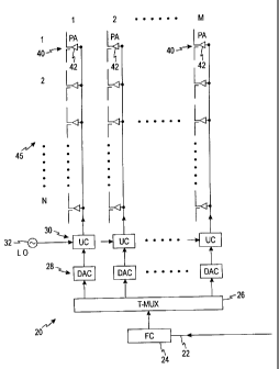
Referring now to the drawings, FIG. 1 shows a transmitter system configuration
2s 20 for a beamformer/smart antenna system, using tower-top mounted
electronics for all
of the RF circuits. The illustrated embodiment takes digital IF (intermediate
frequency)
signals (from an optical carrier or fiber optic cable 22), converts, at a
fiber converter (FC)
24 from optical to a high speed digital signal and at a high speed time
multiplexer (T-
MUX) 26 de-multiplexes the high speed digital signal into M lower speed
digital signals.
3o The transmitter 20 next converts to analog via digital to analog converters
(DAC) 28 and
upconverts, at upconverters (UC) 30, the analog IF signals to RF. The
transmitter 20
then amplifies the signals via a distributed antenna approach, resulting in a
beamformed
CHICAGO 145541 v I 47176-00533CAPT
CA 02340146 2001-03-09
4
collection of signals. This distributed antenna approach, in the embodiment
illustrated in
FIG. 1, comprises an M by N array of antenna elements 40, such as
patch/microstrip
antenna elements, and a power amplifier (PA) 42 closely coupled to each of the
antenna
elements 40, for example, at the feedpoint of each antenna element 40. Thus,
each of the
s upconverters 30 feeds one of M composite antennas, each comprising a total
of N
antenna elements.
In operation, after conversion from fiber (optical IF) to digital, at a
selected data
rate X, the high speed digital signal is de-multiplexed into M streams of
digital signals, at
data rates of X/M. These signals contain the digital beamforming weights and
~o adjustments for phase and amplitude (determined and fixed at a central
processing site -
BTS, MSC, or CO). It will be noted that digital IF signals may be fed to/from
the T-
MUX by a twisted pair or coaxial cable rather than using a fiber optic cable
and converter
as shown in FIG. 1 and the below-described drawings. Also, a DC power
cable/system
for delivering DC power from the ground to the tower top has been omitted in
the
~s drawings for simplicity, but will be understood to be included in such
systems.
The diagram of FIG. 1 shows M columns of N antenna elements forming an
antenna array 45, each connected via a series corporate feed network. Parallel
corporate
feed arrangements could also be used here and throughout the rest of the
described
embodiments hereinbelow. The corporate feed network could be microstrip,
stripline, or
zo RF coaxial cables.
Each antenna element 40 is fed with a power amplifier (PA) module 42, in
similar
fashion to the active/distributed antenna architecture described in the above-
referenced
copending applications.
A common local oscillator (LO) 32 is used for all of the upconverters 30, thus
zs assuring coherent phase for each of the M paths. This LO 32 can be a fixed
frequency
crystal, or a synthesizer.
The fiber optic inputs) 22 to the fiber to digital converter (FC) 24 can be
separate
lines (e.g., multi-mode fiber), or a single line (e.g., single mode fiber).
FIG. 2 shows the tower-top components of FIG. 1 in functional block form
30 (shown on the left hand side of FIG. 2), and (on the right side of FIG. 2)
a ground-based
central processing site (BTS, MSC or CO). In FIG. 2, voice and or data
channels SO are
fed into a DSP block 52 which performs all channel processing (vocoder, code
CHICAGO 14s541v1 47176-00533CAPT
~i
CA 02340146 2004-05-12
spreading/code division multiple access (CDMA), time multiplexing/time
division
multiple access (TDMA}, equalization, etc.) and beamforming and/or spatial
processing.
This block 52 may be referred to as the "Common DSP Block". It is a collection
of DSP
processors, programmed for each specific task (channel and spatial
processing). The
output from this block 52, in either digital baseband (I&Q - in phase and
quadrature) or
digital IF, is converted to an optical carrier via a digital fiber optic (FO)
converter 54. In
one embodiment of the invention, this block 52 and the converter 54 can be
located at the
tower base (cell site) BTS, MSC, or CO (Central Office).
The fiber signals are then carried to the tower via a single cable or
combination of
multimode or singlemode fiber cables, indicated by reference numeral 22.
FIG. 3 shows a receive-only system configuration, for a smart
antenna/beamforming subsystem 120. RF signals are received via an M x N array
of
antenna elements 140, here shown as a collection of patch/microstrip elements.
Each
column in the array is summed via a series corporate feed, which could
alternatively be a
parallel corporate feed. In this particular configuration, the. summed signals
are
amplified,~via a low noise amplifier (LNA) 144, after the corporate feed..
After each
signal is amplified, it is downconverted ~t.a downconverter (DC) 160 to IF,
and digitized
by an analog to digital converter (ADC) 164. The digitized signals are then
time division
multiplexed by a T-MUX 126, into a single high speed digital signal, which is
fed to a
fiber converter (FC) 124, which translatesJmodulates the high speed digital
signal onto an
optical carrier 122. This carrier 122 may be a single, or multiple, fiber
optic cables, for
delivering signals to the BTS, MSC, or CO. Similar to the transmit mode (see
FIG. 1), a
common LO i32 is used to coherently translate all column/array signals from RF
to IF.
The systems of FIGS. 1 and 3 may be combined to form a transmit/receive
system, which
could in turn be combined with the ground-based components of FIG. 2 to define
an
antenna system architecture in accordance with one embodiment of the
invention.
FIG. 4 shows the same basic architecture (a receive-only subsystem 120a) as
FIG.
3, but with an LNA circuidamplifier module 142 at each antenna element 140.
Thus the
signals are amplified prior to being summed via the corporate feeds. This
configuration
may be more expensive, in terms of the costs of the additional LNA components,
but will
achieve increased sensitivity (lower system noise figure} since the signals
are ampIifed
prior to any losses in the corporate feed circuits.
CA 02340146 2001-03-09
6
FIG. 5 shows one embodiment of a transmit/receive smart antenna/beamforming
subsystem 220. This system utilizes a single LNA 244 for each branch (i.e.,
column of
the M x N array), similar to the receive-only configuration of FIG. 3. At each
antenna
element 240, a frequency diplexer (D) 262 is used to separate the transmit and
receive
s power, on separate frequency bands. The receive power is summed, via a
series
corporate feed (could be parallel), and fed to an LNA 244 at the bottom of
each branch
(column, i.e., of the M x N array). The amplified RF signals are then
downconverted to
IF at downconverters (DC) 260 and digitized at A/D converters 264, and fed to
the high
speed T-MUX (time domain multiplexes) 226. Similarly, transmit mode signals
(from
io the BTS, MSC, or CO) are converted, de-multiplexed, digitized, and
upconverted from
IF to RF at FC 224, T-MUX 226, DACs 228 and UCs 230. The converted signals are
then distributed to the antenna elements, on each branch, via the corporate
feed (series or
parallel) and amplified (at each antenna element 240) by PAs 242. The
amplified signals
pass through the frequency diplexer (D) 262 to the antennas 240 to be radiated
into
i s space. The same LO source 232 can be used for both the upconversion and
downconversion operations, for all of the branches.
The fiber optic cables 222 thus carry digital IF on an optical carrier in both
directions. This can be accomplished on a single FO (fiber optic) cable via
wavelength
division multiplexing, or on multiple FO cables, one (or more) for each path.
zo FIG. 6 shows a similar architecture to FIG. 5 for a transmit/receive system
220a,
except that the receive mode signals (uplink) are amplified by LNAs 244 at the
antenna
elements 240, before summing in the corporate feed network. This is similar to
the
receive-only configuration of FIG. 4.
FIG. 7 shows a basic architecture for the tower-top beamformer subsystem, for
all
Zs of the embodiments of FIGS. 1-6. A panel antenna system 300, with a fiber
converter
(FC) 324, is shown with fiber optic transmission lines) or cables) 322. The
subsystem
300 may include all of the components of any of the subsystems of FIGS. 1-6,
up to the
FC (fiber converter) 324. The advantage of this arrangement is that all of the
RF
functionality is performed at a single location, i.e. at the tower top. This
minimizes the
30 lengths of RF transmission lines throughout the system. For example, there
is no need to
transmit RF back to the base station (BTS), MSC or CO 310. This results in
minimizing
ohmic and power losses, as well as increasing the overall system performance
(noise
CHICAGO 14S541v1 47176-00533CAPT
CA 02340146 2001-03-09
7
figure, etc.). This is also the part of the system that is most likely to
remain static (i.e.
not requiring performance-oriented changes as often).
The section of the beamforming system that will likely change, due to improved
DSP availability and algorithms, software updates, etc. can be centralized in
a single
s location 310 (e.g., BS/BTS, MSC, or CO). This section may include
beamformer, digital
signal processing (DSP) and channel processing components as indicated by
reference
numberal 352 in Fig.7.
At the other end of the fiber cable 322 is a fiber converter (FC) 354 to
convert to
digital IF, and a digital multiplexer 312, which may be part of the base
station 310. The
io above-described arrangement allows all the high cost "digital processing"
segment of the
beamformer to be placed in a central location, to facilitate algorithm and
software
upgrades, as well as hardware (DSP) changes.
FIG. 8 shows an architectural approach for microwave backhaul link to replace
the fiber connection 22 ( 122, 222, 322). All of the prior embodiments
described the
is high-speed backhaul link being performed using fiber optic cable. However,
currently
many cell sites use microwave (2 - 40 GHz range) links for the
trunking/backhaul, and
this may be substituted for the fiber link shown in the above-described
embodiments
without departing from the invention.
In FIG. 8, on the top left, is a block 300 denoted as "RF circuits". This
zo encompasses the antenna elements, LNAs, PA's, corporate feed networks, RF
upconverters and downconverters, as well as A/Ds and DACs shown in the above-
described embodiments. The digital signal is then fed into a composite high
speed digital
T-MUX 326 (as shown in the previous embodiments). However, rather than feed
the
time division digitally multiplexed signals into a fiber converter, the
signals are directly
zs translated, at the tower top, by a microwave (MW) converter (transceiver)
313, and
amplified through a PA (power amplifier) 317, fed through a microwave
frequency
diplexer (D) 321, to a radiating backhaul antenna 323. This backhaul antenna
323 is
similar to a terrestrial microwave antenna, or LMDS (local multipoint
distribution
service) antenna system. Similarly received uplink microwave signals, from the
antenna
30 323, are fed back through the frequency diplexer (D) 321, amplified via a
microwave
LNA 319, and downconverted to digital IF (high speed), back to the high speed
T-MUX
326.
CHICAGO 145541 v I 47176-00533CAPT
~i
CA 02340146 2004-05-12
Optionally, the high speed digital multiplexed signals from the
beamformer/smart
antenna subsystem 320 could be fed to an intermediate modulator (MOD) 315
(shown in
phantom line), that modulates the IF signals to a format more efficient for
microwave
transmission, and then fed to the microwave converter 313.
FIGS. .9-13 are respectively similar to FIGS. 1 and 3-6, however, FIGS. 9-13
show third generation PCS and UMTS (universal mobile telecommunications
service)
(3G) systems. Two standards, designated as CDMA-2000 and W-CDMA, are currently
being developed for use as the worldwide roaming or mobile (celluIarized)
systems for
voice and data transport. While architecturally very similar to the diagrams
in FIGS. 1
and 3-6, FIGS. 9-13 differ in that they use a QPSK (quadrature phase shift
keying)
modulator and RF upconverter block, designated in FIGS. 9-13 as a 3G (third
generation
CDMA) modulator block 410 (510, 610). This block assumes digital baseband I &
Q on
the input (or output). Therefore, digital baseband (I&Q) signaling is embedded
in the
fiber optic signal, which is assumed to .be time division multiplexed.
FIG. 9 shows a 3G transmit mode smart antenna/beamformer subsystem 420.
The digital multiplexed (baseband I & Q) signals, carried on a high speed
stream, are
converted from fiber to digital at FC 424 and de-multiplexed at T-MUX 426 into
M
lower speed streams. The 3G modulator block 410, on each branch, converts the
signals
from digital to analog, performs a QPSK modulation, spreads the carriers (via
the
appropriate CDMA spreading codes) and upconverts to RF. The rest of FIG. 9 is
similar
to FIG. 1. Also, aII 3GM blocks 410 use the same local oscillator 432 to
coherently
upconvert to all branches.
FIG. 10 shows a receive mode configuration 520, with a single LNA 544 at the
output of the corporate feed foi each branch. A 3G modulator block 510 has
been
separated into two blocks, a "demodulator" (downconverter, CDMA code
despreader,
and QPSK demodulator) 560 and an A/D 564. The digital baseband (I & Q) outputs
are
then time division multiplexed at T-MUX 526, and fed to the digital to fiber
converter
(FC) 524, which sends the multiplexed digital baseband signals on a fiber
carrier 522.
FIG. 11 shows a second receive mode configuration 520a, with an LNA 542 at
each antenna element 540, prior to the corporate feed network on each branch,
end is
otherwise the same as FIG. 10.
CA 02340146 2001-03-09
9
FIGS. 12 and 13 shows two configurations 620, 620a for a transmit/receive 3G
beamformer/smart antenna system, with a 3G modulator block 610, 612 on each
path (2-
Way) on each branch. FIG. 12 shows a configuration with a single LNA 644 on
each
receive branch. FIG. 13 shows a configuration with an LNA 644 at each antenna
element
s prior to the corporate feed network. In FIGS. 12 and 13, components similar
to those
used in the above-described embodiments are designated by similar reference
numerals
with the prefix 6. Also in FIGS. 12 and 13, the 3G modulator block 610
includes the
components of both the 3G modulator blocks 410 and 510 of FIGS. 9 and 10, as
described above.
m While the systems of FIGS. 9-13 illustrate a fiber carrier 422, 522, etc.,
each
could alternatively use a microwave backhaul link of the type shown in FIG. 8.
While particular embodiments and applications of the present invention have
been illustrated and described, it is to be understood that the invention is
not limited to
the precise construction and compositions disclosed herein and that various
is modifications, changes, and variations may be apparent from the foregoing
descriptions
without departing from the spirit and scope of the invention as defined in the
appended
claims.
CHICAGO 145541 v I 47176-OOS33CAPT