Note: Descriptions are shown in the official language in which they were submitted.
CA 02340228 2001-02-12
WO 00/09757 PCT/US99/18438
OPTICALLY CHARACTERIZING POLYMERS
Field of the Invention
The present invention is directed to optical systems, methods and products for
analyzing polymers, and more particularly to optical systems, methods and
products that
utilize highly localized optical radiation for characterizing individual units
of polymers.
Back~ro,-, and
This patent application claims priority from U.S. Provisional Application
60/096,544
t o filed on August 13, 1998, and U.S. Provisional Application 60/120,414
filed on February 14,
1999, both of which are incorporated by reference.
Cells have a complex microstructure that determine the functionality of the
cell. Much
of the diversity associated with cellular structure and function is due to the
ability of a cell to
assemble various building blocks into diverse chemical compounds. The cell
accomplishes
15 this task by assembling polymers from a limited set of building blocks
referred to as
monomers or units. The key to the diverse functionality of polymers is based
in the primary
sequence of the monomers within the polymer and is integral to understanding
the basis for
cellular function, such as why a cell differentiates in a particular manner or
how a cell will
respond to treatment with a particular drug.
2o The ability to identify the structure of polymers by identifying their
sequence of
monomers is integral to the understanding of each active component and the
role that
component plays within a cell. By determining the sequences of polymers it is
possible to
generate expression maps, to determine what proteins are expressed, to
understand where
mutations occur in a disease state, and to determine whether a polysaccharide
has better
25 function or loses function when a particular monomer is absent or mutated.
Expression maps relate to determining mRNA expression patterns. The need to
identify differentially expressed mRNAs is critical in the understanding of
genetic
programming, both temporally and spatially. Different genes are turned on and
off during the
temporal course of an organisms' life development, comprising embryonic,
growth, and aging
3o stages. In addition to developmental changes, there are also temporal
changes in response to
varying stimuli such as injury, drugs, foreign bodies, and stress. The ability
to chart
expression changes for specific sets of cells in time either in response to
stimuli or in growth
CA 02340228 2001-02-12
WO 00/09?5? PCT/US99/18438
-2
allows the generation of what are called temporal expression maps. On the
other hand, there
are also body expression maps, which include knowledge of differentially
expressed genes for
different tissues and cell types. Since generation of expression maps involve
the sequencing
and identification of cDNA or mRNA, more rapid sequencing necessarily means
more rapid
generation of multiple expression maps.
Currently, only 1 % of the human genome and an even smaller amount of other
genomes have been sequenced. In addition, only one very incomplete human body
expression
map using expressed sequence tags has been achieved (Adams et al., 1995).
Current protocols
for genomic sequencing are slow and involve laborious steps such as cloning,
generation of
genomic libraries, colony picking, and sequencing. The time to create even one
partial
genomic library is on the order of several months. Even after the
establishment of libraries,
there are time lags in the preparation of DNA for sequencing and the running
of actual
sequencing steps. Given the multiplicative effect of these unfavorable facts,
it is evident that
the sequencing of even one genome requires an enormous investment of money,
time, and
effort.
In general, DNA sequencing is performed using one of two methods. The first
and
more popular method is the dideoxy chain termination method described by
Sanger et al.
("DNA sequencing with chain-terminating inhibitors," Proc. Natl. Acad. Sci.
USA. 74:5463-
7, 1977). This method involves the enzymatic synthesis of DNA molecules
terminating in
2o dideoxynucleotides. By using the four ddNTPs, a population of molecules
terminating at each
position of the target DNA can be synthesized. Subsequent analysis yields
information on the
length of the DNA molecules and the base at which each molecule terminates
(either A, C, G,
or T). With this information, the DNA sequence can be determined. The second
method is
Maxam and Gilbert sequencing (Maxam and Gilbert, "A new method for sequencing
DNA,"
Proc. Natl. Acad Sci. USA. 74:560-4, 1977), which uses chemical degradation to
generate a
population of molecules degraded at certain positions of the target DNA. With
knowledge of
the cleavage specificities of the chemical reactions and the lengths of the
fragments, the DNA
sequence is generated. Both methods rely on polyacrylamide gel electrophoresis
and
photographic visualization of the radioactive DNA fragments. Each process
takes about 1-3
3o days. The Sanger sequencing reactions can only generate 300-800 bases in
one run.
Sanger-based methods have been proposed to improve the output of sequence
information. The Sanger-based methods include multiplex sequencing, capillary
gel
electrophoresis, and automated gel electrophoresis. Recently, there has also
been increasing
CA 02340228 2001-02-12
WO 00/09757 PCT/US99/18438
-3-
interest in developing Sanger independent methods as well. Sanger independent
methods use a
completely different methodology to realize the base information. This
category contains the
most novel techniques, which include scanning electron microscopy (STM), mass
spectrometry, enzymatic luminometric inorganic pyrophosphate detection assay
(ELIDA)
sequencing, exonuclease sequencing, and sequencing by hybridization.
Currently, automated gel electrophoresis is the most widely used method of
large-scale
sequencing. Automation requires reading of fluorescently labeled Sanger
fragments in real
time with a charge coupled device (CCD) detector. The four different dideoxy
chain
termination reactions are run with different labeled primers. The reaction
mixtures are
1 o combined and co-electrophoresed down a slab of polyacrylamide. Using laser
excitation at
the end of the gel, the separated DNA fragments are resolved and the sequence
determined by
computer. Many automated machines are available commercially, each employing
different
detection methods and labeling schemes. The most efficient of these is the
Applied
Biosystems Model 377XL, which generates a maximum actual rate of 115,200 bases
per day.
~ 5 In the method of capillary gel-electrophoresis, reaction samples are
analyzed by small
diameter, gel-filled capillaries. The small diameter of the capillaries (50
pm) allows for
efficient dissipation of heat generated during electrophoresis. Thus, high
field strengths can
be used without excessive Joule heating (400 V/m), lowering the separation
time to about 20
minutes per reaction run. Not only are the bases separated more rapidly, there
is also
2o increased resolution over conventional gel electrophoresis. Furthermore,
many capillaries are
analyzed in parallel (Wooley and Mathies, "Ultra-high-speed DNA sequencing
using capillary
electrophoresis chips," Anal. Chem. 67:3676-3680, 1995), allowing
amplification of base
information generated (actual rate is equal to 200,000 bases/day). The main
drawback is that
there is not continuous loading of the capillaries since a new gel-filled
capillary tube must be
25 prepared for each reaction. Capillary gel electrophoresis machines have
recently been
commercialized.
Multiplex sequencing is a method which more efficiently uses electrophoretic
gels
(Church and Kieffer-Higgins, "Multiplex DNA sequencing," Science. 240:185-88,
1988).
Sanger reaction samples are first tagged with unique oligomers and then up to
20 different
3o samples are run on one lane of the electrophoretic gel. The samples are
then blotted onto a
membrane. The membrane is then sequentially probed with oligomers that
correspond to the
tags on the Sanger reaction samples. The membrane is washed and reprobed
successively
until the sequences of all 20 samples are determined. Even though there is a
substantial
CA 02340228 2001-02-12
WO 00/09757 PCT/US99/18438
-4
reduction in the number of gels run, the washing and hybridizing steps are as
equally
laborious as running electrophoretic gels. The actual sequencing rate is
comparable to that of
automated gel electrophoresis.
Sequencing by mass spectrometry was first introduced in the late 80's. Recent
developments in the field have allowed for better sequence determination
(Grain,
MassSpectrom. Rev. 9:505-54, 1990; Little et al., J. Am. Chem. Soc. 116:4893-
4897, 1994;
Keough et al., Rapid Commun. Mass Spectrom. 7:195-200, 1993; Smirnov et al.,
1996). Mass
spectrometry sequencing first entails creating a population of nested DNA
molecules that
differ in length by one base. Subsequent analysis of the fragments is
performed by mass
i o spectrometry. In one example, an exonuclease is used to partially digest a
33-mer (Smirnov,
"Sequencing oligonucleotides by exonuclease digestion and delayed extraction
matrix-
assisted laser desorption ionization time-of flight mass spectrometry," Anal.
Biochem. 238:19-
25, 1996). A population of molecules with similar 5' ends and varying points
of 3'
termination is generated. The reaction mixture is then analyzed. The mass
spectrometer is
15 sensitive enough to distinguish mass differences between successive
fragments, allowing
sequence information to be generated.
Mass spectrometry sequencing is highly accurate, inexpensive, and rapid
compared to
conventional methods. The major limitation, however, is that the read length
is on the order
of tens of bases. Even the best method, matrix-assisted laser desorption
ionization time-of
2o flight (MALDI-TOF) mass spectroscopy (Smirnov et al., "Sequencing
oligonucleotides by
exonuclease digestion and delayed extraction matrix-assisted laser desorption
ionization time-
of flight mass spectrometry," Anal. Biochem. 238:19-25, 1996), can only
achieve maximum
read lengths of 80-90 base pairs. Much longer read lengths are physically
impossible due to
fragmentation of longer DNA at guanidines during the analysis step. Mass
spectrometry
25 sequencing is thus limited to verifying short primer sequences and has no
practical application
in large-scale sequencing.
The Scanning tunneling microscope (STM) sequencing (Ferrell, "Scanning
tunneling
microscopy in sequencing of DNA." In Molecular Biology and Biotechnology, R.A.
Meyers,
Ed. VCH Publishers, New York, 1997) method was conceived at the time the STM
was
3o commercially available. The initial promise of being able to read base-pair
information
directly from the electron micrographs no longer holds true. DNA molecules
must be placed
on conducting surfaces, which are usually highly ordered pyrolytic graphite
(HOPG) or gold.
These lack the binding sites to hold DNA strongly enough to resist removal by
the physical
CA 02340228 2001-02-12
WO 00/09757 PCTNS99/18438
-5-
and electronic forces exerted by the tunneling tip. With difficulty, DNA
molecules can be
electrostatically adhered to the surfaces. Even with successful immobilization
of the DNA, it
is difficult to distinguish base information because of the extremely high
resolutions needed.
With current technology, purines can be distinguished from pyrimidines, but
the individual
purines and pyrimidines cannot be identified. The ability to achieve this feat
requires electron
microscopy to be able to distinguish between aldehyde and amine groups on the
purines and
the presence or absence of methyl groups on the pyrimidines.
Enzymatic luminometric inorganic pyrophosphate detection assay (ELIDA)
sequencing uses the detection of pyrophosphate release from DNA polymerization
to
t o determine the addition of successive bases. The pyrophosphate released by
the DNA
polymerization reaction is converted to ATP by ATP sulfurylase and the ATP
production is
monitored continuously by firefly luciferase. To determine base specificity,
the method uses
successive washes of ATP, CTP, GTP, and TTF. If a wash for ATP generates
pyrophosphate,
one or more adenines are incorporated. The number of incorporated bases is
directly
proportional to the amount of pyrophosphate generated. Enhancement of
generated sequence
information can be accomplished with parallel analysis of many ELIDA reactions
simultaneously.
Exonuclease sequencing involves a fluorescently labeled, single-stranded DNA
molecule which is suspended in a flowing stream and sequentially cleaved by an
exonuclease.
2o Individual fluorescent bases are then released and passed through a single
molecule detection
system. The temporal sequence of labeled nucleotide detection corresponds to
the sequence
of the DNA (Ambrose et al., "Application of single molecule detection to DNA
sequencing
and sizing," Ber. Bunsenges. Phys. Chem. 97:1535-1542, 1993; Davis et al.,
"Rapid DNA
sequencing based on single-molecule detection," Los Alamos Science. 20:280-6,
1992; 3ett et
al., "High-speed DNA sequencing: an approach based upon fluorescence detection
of single
molecules," J. OfBio. Structure & Dynamics. 7:301-9, 1989). Using a processive
exonuclease, it theoretically is possible to sequence 10,000 by or larger
fragments at a rate of
10 bases per second.
In the sequencing by hybridization method, a target DNA is sequentially probed
with a
3o set of oligomers consisting of all the possible oligomer sequences. The
sequence of the target
DNA is generated with knowledge of the hybridization patterns between the
oligomers and
the target (Bains, "Hybridization methods for DNA sequencing," Genomics.
11:294-301,
1991; Cantor et al., "Reporting on the sequencing by hybridization workshop,"
Genomics.
CA 02340228 2001-02-12
WO 00/09757 PCTNS99/18438
-6-
13:1378-1383, 1992; Drmanac et al., "Sequencing by hybridization." In
Automated DNA
Sequencing and Analysis Techniques, J. Craig Ventor, Ed. Academic Press,
London, 1994).
There are two possible methods of probing target DNA. The "Probe Up" method
includes
immobilizing the target DNA on a substrate and probing successively with a set
of oligomers.
"Probe Down" on the other hand requires that a set of oligomers be immobilized
on a
substrate and hybridized with the target DNA. With the advent of the "DNA
chip," which
applies microchip synthesis techniques to DNA probes, arrays of thousands of
different DNA
probes can be generated on a 1 cmz area, making Probe Down methods more
practical. Probe
Up methods would require, for an 8-mer, 65,536 successive probes and washings,
which
would take an enormous amount of time. On the other hand, Probe Down
hybridization
generates data in a few seconds. With perfect hybridization, 65,536 octamer
probes would
determine a maximum of 170 bases. With 65,536 "mixed" 11-mers, 700 bases can
be
generated.
The most common limitation of most of these techniques is a short read length.
In
~ 5 practice a short read length means that additional genetic sequence
information needs to be
sequenced before the linear order of a target DNA can be deciphered. The short
fragments
have to be bridged together with additional overlapping fragments.
Theoretically, with a 500
base read length, a minimum of 9 x 10⁹ bases need to be sequenced before the
linear sequence
of all 3 x 10⁹ bases of the human genome are properly ordered. In reality, the
number of bases
2o needed to generate a believable genome is approximately 2 x 10'°
bases. Comparisons of the
different techniques show that only the impractical exonuclease sequencing has
the theoretical
capability of long read lengths. The other methods have short theoretical read
lengths and
even shorter realistic read lengths. To reduce the number of bases that need
to be sequenced,
it is clear that the read length must be improved.
25 Protein sequencing generally involves chemically induced sequential removal
and
identification of the terminal amino acid residue, e.g., by Edman degradation.
See Stryer, L.,
Biochemistry, W. H. Freeman and Co., San Francisco (1981) pp. 24-27. Edman
degradation
requires that the polypeptide have a free amino group which is reacted with an
isothiocyanate.
The isothiocyanate is typically phenyl isothiocyanate. The adduct
intramolecularly reacts with
3o the nearest backbone amide group of the polymer thereby forming a five
membered ring. This
adduct rearranges and the terminal amino acid residue is then cleaved using
strong acid. The
released phenylthiohydantoin (PTH) of the amino acid is identified and the
shortened polymer
can undergo repeated cycles of degradation and analysis.
CA 02340228 2001-02-12
WO 00/09757 PCT/US99/18438
_7-
Further, several new methods have been described for carboxy terminal
sequencing of
polypeptides. See Inglis, A. S., Anal. Biochem. 195:183-96 (1991). Carboxy
terminal
sequencing methods mimic Edman degradation but involve sequential degradation
from the
opposite end of the polymer. See Inglis, A. S., Anal. Biochem. 195:183-96
(1991). Like
s Edman degradation, the carboxy-terminal sequencing methods involve
chemically induced
sequential removal and identification of the terminal amino acid residue.
More recently, polypeptide sequencing has been described by preparing a nested
set
(sequence defining set) of polymer fragments followed by mass analysis. See
Chait, B. T. et
al., Science 257:1885-94 (1992). Sequence is determined by comparing the
relative mass
to difference between fragments with the known masses of the amino acid
residues. Though
formation of a nested (sequence defining) set of polymer fragments is a
requirement of DNA
sequencing, this method differs substantially from the conventional protein
sequencing
method consisting of sequential removal and identification of each residue.
Although this
method has potential in practice it has encountered several problems and has
not been
~ s demonstrated to be an effective method.
Each of the known methods for sequencing polymers has drawbacks. For instance
most of the methods are slow and labor intensive. The gel based DNA sequencing
methods
require approximately 1 to 3 days to identify the sequence of 300-800 units of
a polymer.
Methods such as mass spectroscopy and ELIDA sequencing can only be performed
on very
2o short polymers.
A need exists for de noveau polymer sequence determination. The rate of
sequencing
has limited the capability to generate multiple body and temporal expression
maps which
would undoubtedly aid the rapid determination of complex genetic function. A
need also
exists for improved systems and methods for analyzing polymers in order to
speed up the rate
25 at which diagnosis of diseases and preparation of new medicines is carried
out.
Summary of the Invention
The invention relates to new systems, methods and products for analyzing
polymers
and in particular new systems, methods and products useful for determining the
sequence of
3o polymers. The invention has numerous advantages over prior art systems and
methods used
to sequence polymers. Using the methods of the invention the entire human
genome could be
sequenced several orders of magnitude faster than could be accomplished using
conventional
technology. In addition to sequencing the entire genome, the systems, methods
and products
CA 02340228 2001-02-12
WO 00/09757 PCT/US99/18438
_g_
of the invention can be used to create comprehensive and multiple expression
maps for
developmental and disease processes. The ability to sequence an individual's
genome and to
generate multiple expression maps will greatly enhance the ability to
determine the genetic
basis of any phenotypic trait or disease process.
According to one aspect, a system for optically analyzing a polymer of linked
units
includes an optical source, an interaction station, an optical detector, and a
processor. The
optical source is constructed to emit radiation of a selected wavelength. The
interaction
station is constructed to receive the emitted radiation and produce a
localized radiation spot
from the radiation emitted from the optical source. The interaction station is
also constructed
t o to sequentially receive units of the polymer and arranged to irradiate
sequentially the units at
the localized radiation spot. The optical detector is constructed to detect
radiation including
characteristic signals resulting from interaction of the localized radiation
spot with the units.
The processor is constructed and arranged to analyze the polymer based on the
detected
radiation.
t 5 Preferred embodiments of this aspect include one or more of the following
features:
The interaction station is constructed to sequentially receive the units being
selectively
labeled with a radiation sensitive label and the interaction includes
interaction of the localized
radiation with the radiation sensitive label.
The radiation sensitive label includes a fluorophore.
2o The interaction station includes a waveguide constructed to receive the
emitted
radiation and provide the evanescent radiation in response thereto.
The interaction station includes a slit having a width in the range of 1 nm to
500 nm,
wherein the slit produces the localized radiation spot.
The interaction station includes a microchannel and a slit having a submicron
width
25 arranged to produce the localized radiation spot. The microchannel is
constructed to receive
and advance the polymer units through the localized radiation spot.
The width of the slit is in the range of 10 nm to 100 nm.
The system may include a polarizer and the optical source is a laser
constructed to emit a
beam of radiation and the polarizer is arranged to polarize the laser beam
prior to reaching the
30 slit.
The polarizer may be arranged to polarize the laser beam in parallel to the
width of the slit,
or perpendicular to the width of the slit.
The interaction station may include several slits located perpendicular to the
microchannel
CA 02340228 2001-02-12
WO 00/09757 PCT/US99/18438
-9-
that is arranged to receive the polymer in a straightened form.
The interaction station may include a set of electrodes constructed and
arranged to provide
electric field for advancing the units of the polymer through the
microchannel.
The system may further include an alignment station constructed and arranged
to
straighten the polymer and provide the straightened polymer to the interaction
station.
In another embodiment a method for optically analyzing a polymer of linked
units
comprising:
labeling selected units of the polymer with radiation sensitive labels;
sequentially passing the units of the polymer through a microchannel;
I o generating radiation of a selected wavelength to produce therefrom a
localized radiation
spot;
irradiating sequentially the labeled units of the polymer at the localized
radiation spot;
detecting sequentially radiation providing characteristic signals resulting
from interaction
of the localized radiation spot with the labels or the units; and
15 analyzing the polymer based on the detected radiation.
In another embodiment, an article of manufacture used for optically analyzing
a
polymer of linked units, comprising an interaction station fabricated on a
substrate and
constructed to receive radiation and produce therefrom a localized radiation
spot. The
interaction station is further constructed to sequentially receive units of
the polymer and
2o arranged to irradiate sequentially the units at the localized radiation
spot to generate
characteristic signals of radiation.
According to another aspect, a system for optically analyzing a polymer of
linked units
includes an optical source, an interaction station, an optical detector, and a
processor. The
optical source is constructed to emit radiation of a selected wavelength. The
interaction
25 station is constructed to receive the emitted radiation and constructed to
sequentially receive
units of the polymer and arranged to irradiate sequentially the units of the
polymer with
evanescent radiation excited by the radiation emitted from the source. The
optical detector
is constructed to detect radiation including characteristic signals resulting
from interaction
of the evanescent radiation with the units. The processor is constructed and
arranged to
3o analyze the polymer based on the detected radiation.
Preferred embodiments of this aspect include one or more of the following
features:
The interaction station is constructed to sequentially receive the units being
selectively labeled with a radiation sensitive label and the interaction
includes interaction of
CA 02340228 2001-02-12
WO 00/09757 PCT/US99/18438
- 10-
the evanescent radiation with the radiation sensitive label.
The radiation sensitive label includes a fluorophore.
The interaction station includes a waveguide constructed to receive the
emitted
radiation and provide the evanescent radiation in response thereto.
The waveguide is a dielectric waveguide constructed to achieve total internal
reflection of introduced light. The waveguide is a rectangular mirror
waveguide with a
dielectric surrounded by metallic mirror layers constructed to have a low loss
of introduced
light. The waveguide includes a tip including an aperture in the metallic
mirror layers and
arranged to emit the evanescent radiation. The waveguide includes a tip
constructed to emit
t o the evanescent radiation.
The interaction station includes a nanochannel located at the tip of the
waveguide
and arranged to receive the polymer in a straightened form.
The interaction station includes a set of electrodes constructed and arranged
to
provide electric field for advancing the units of the polymer through the
nanochannel. The
15 electrodes are internal electrodes.
The electrodes are external electrodes. The nanochannel is between 2 and 50
nanometers.
The waveguide is further constructed and arranged to receive the radiation
including
the characteristic signals and optically couple the received radiation to the
optical detector.
2o The interaction station includes another waveguide constructed and arranged
to receive
the radiation including the characteristic signals and optically couple the
received radiation to
the optical detector.
The system further includes an alignment station constructed and arranged to
straighten
the polymer and provide the straightened polymer to the interaction station.
25 In yet another aspect the invention is a system for optically analyzing a
polymer utilizing
confocal fluorescence illumination of linked units. The system includes an
optical source
constructed to emit optical radiation; a filter constructed to receive and
filter said optical
radiation to a known wavelength; a dichroic mirror constructed to receive said
filtered optical
radiation; an interaction station constructed to receive said filtered optical
radiation and
3o produce a localized radiation spot from said filtered optical radiation,
said interaction station
being also constructed to sequentially receive units of said polymer and
arranged to irradiate
sequentially said units at said localized radiation spot; an optical detector
constructed to
detect radiation including characteristic signals resulting from interaction
of said units at said
CA 02340228 2001-02-12
WO 00/09757 PCT/US99/18438
-11-
localized radiation spot; and a processor constructed and arranged to analyze
said polymer
based on said detected radiation including said characteristic signals.
In one embodiment the interaction station is constructed to sequentially
receive said units
being selectively labeled with a radiation sensitive label producing said
characteristic signals
at said localized radiation spot. In another embodiment the radiation
sensitive label includes a
fluorophore. In some embodiments the filter is a laser line filter.
The system may also include an objective, wherein the objective focuses said
filtered
optical radiation.
The proposed system and method for analyzing polymers is particularly useful
for
1 o determining the sequence of units within a DNA molecule and can eliminate
the need for
generating genomic libraries, cloning, and colony picking, all of which
constitute lengthy pre-
sequencing steps that are major limitations in current genomic-scale
sequencing protocols.
The methods disclosed herein provide much longer read lengths than achieved by
the prior arrt
and a million-fold faster sequence reading. The proposed read length is on the
order of
15 several hundred thousand nucleotides. This translates into significantly
less need for
overlapping and redundant sequences, lowering the real amount of DNA that
needs to be
sequenced before genome reconstruction is possible. The actual time taken to
read a given
number of units of a polymer is a million-fold more rapid than current methods
because of the
tremendous parallel amplification supplied by a novel apparatus also claimed
herein, which is
2o referred to as a nanochannel plate or a microchannel plate. The combination
of all these
factors translates into a method of polymer analysis including sequencing that
will provide
enormous advances in the field of molecular and cell biology.
Brief Description of the Drawings_
25 Fig. 1 illustrates diagrammatically a system for characterizing polymers.
Fig. 2 illustrates an alignment and a first interaction station used in the
system of Fig. 1.
Fig. 3 is a cross-sectional view of the alignment and the first interaction
station along lines
3-3 shown in Fig. 2.
Fig. 4 is a top view of a portion of the alignment and the first interaction
station shown in
3o Fig. 2.
Fig. 4A illustrates the arrangement of a nanoslit located in the first
interaction station
shown in Fig 4.
Fig. 4B illustrates an optical system for characterizing polymer units labeled
by a
CA 02340228 2001-02-12
WO 00/09757 PCT/US99/18438
- 12-
fluorophore.
Figs. S and SA illustrate a second interaction station used in the system of
Fig. 1.
Figs. 6 through 7B illustrate the fabrication of the alignment and first
interaction station
shown in Fig 4.
s Fig. 8 is an SEM micrograph of the fabricated alignment and first
interaction stations.
Figs. 9, 10A, 1 OB, and l0C show results of a test measurement of the
alignment and
interaction station of Fig. 8.
Fig. 11 is a cross-sectional view of the central line of optical waveguides
according to
another embodiment of the first interaction station.
t o Fig. 11 A is a perspective view of the optical waveguides shown in Fig. 11
Figs. I 1 B and 1 I C illustrate the interaction of with a linearized polymer
with evanescent
radiation emitted from the optical waveguide.
Fig. 12 illustrates optical systems for near-field and far-field detection as
used with the
optical waveguide of Fig. 11.
~s Figs. 13, 13A and 13B illustrate coupling of electromagnetic radiation into
the optical
waveguide of Fig. I 1.
Figs. 14A through 16G illustrate the fabrication of the optical waveguides
shown in Fig.
11.
Fig. 17 is a schematic of an optical apparatus which utilizes confocal
fluorescence
2o illumination and detection for linear analysis of polymers.
Fig. 18 is a top view of another embodiment of the alignment station for
aligning and
stretching polymer.
25 ~e~~iled Descri tion of lrhe Preferred Embodiments
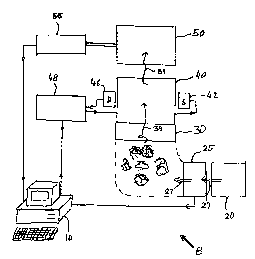
Referring to Fig. l, an interactive system for characterizing individual units
of a
polymer includes a system controller 10, a polymer supply 20, a microfluidic
pump 25, a
polymer alignment station 30, a first interaction station 40, and a second
interaction station
50. System controller 10 may be a general purpose computer. Microfluidic pump
25 supplies
3o selected amounts of polymer 27 from polymer supply 20 to polymer alignment
station 30.
Polymer alignment station 30, controlled by system controller 10, straightens
and aligns
individual polymers using force field and mechanical obstacles, and dispenses
the polymers to
first interaction station 40. The first interaction station 40 uses an optical
system for
CA 02340228 2001-02-12
WO 00/09757 PC'f/US99/18438
_1;_
characterizing individual units of the polymer passim through. The optical
system includes
an optical source 42. an optical filter 45, an optical detector 46 and other
optical elements and
electronic elements associated with the source and detector. The optical
system is controlled
by an optical controller 48.
5 As the individual units of the polymer pass through interaction station 40,
optical source
42 emits radiation directed to an optical component of interaction station 40.
The optical
component produces a localized radiation spot that interacts directly with
polymer units. or
interacts with labels selectively attached to the polymer units, or interact
with both the
polymer units and the labels. The localized radiation spot includes non-
radiating near field or
an evanescent wave, localized in at least one dimension. The localized
radiation spot pro~~ides
a much higher resolution than the diffraction-limited resolution used in
conventional optics.
Furthermore, interaction station 40 uses unique arrangements and geometries
that allow
the localized radiation spot to interact with one or several polymer units or
attached labels that
are on the order of nanometers or smaller. Optical detector 46 detects light
modified by the
is interaction and provides a detection signal to optical controller .18.
Second interaction station
~0 uses electric or electromagnetic field, X-ray radiation, or visible or
infrared radiation for
characterizing the polymer passing from first interaction station 40 through
second interaction
station 50. A controller ~6 controls the operation of second interaction
station 50. Both
controllers 48 and 56 are connected to system controller ! 0.
20 Referring to Figs. 2 and 3. polymer alignment station 30 and first
interaction station 40
include a substrate 92, a quartz wafer 60, and a glass cover 90, which is
optional. Substrate 9?
is machined from a non-conducting, chemical( inert material, such as Teflon~R~
or Delrin R . to
facilitate a flow of conducting fluid 96 (for example, agarose gel) and the
examined polymer.
Substrate 92 includes trenches 94A and 94B machined to receive gold wires 98A
and 98B.
i5 respectively, which have a selected shape in accordance with the shape of
the electric field
used for advancing polymer molecules 39 across first interaction station 40.
Quartz wafer 60
is sealed onto substrate 92 around regions 91.
Alternatively. trenches 94A and 94B and wires 98A and 98B may be replaced by
metallic
regions located directly on quartz wafer 60, or may be replaced by external
electrodes for
3o creating the electric field. In general, the electrodes are spaced apart
over a distance in the
range of about millimeter to 5 centimeters, and preferably 2 centimeters and
provide typically
field strengths of about 20 V/cm.
Figs. 4 and 4A show a presently preferred embodiment of alignment station 30
and first
RECTIFIED SHEET (RULE 91)
ISA/EP
CA 02340228 2001-02-12
WO 00/09757 PCT/US99/18438
-l-1-
Interaction station 40. Fig. 4 is a top view of a portion of alignment station
30 and first
interaction station 40 (also shown in Fig. 2), which are fabricated on quartz
wafer 60. Of
course, a single quartz wafer 60 may include hundreds or thousands of the
alignment and first
interaction stations. Quartz wafer 60 includes a quartz substrate covered with
a metal layer 6?
(e.g. aluminum, gold, silver) and having a microchannel 41 fabricated on the
surface. .
Fabricated through metal layer 62 are slits 36A. 36B and 36C. which form the
optical
elements that provide the localized radiation spot. Slits 36A. 36B and 36C
have a selected
width in the range ber<veen 1 nm and 5000 nm. and preferably in the range
between 10 nm
and 1000 nm. and more preferably in the range between 10 nm and 100 nm. Slits
36A. 36B
to and 36C are located across microchannel -11, which has a width in the range
of 1 micrometer
to 50 micrometers and a length of several hundred micrometers. The electric
field, created by
gold wires 98A and 98B, pulls a polymer chain 39 (such as a DNA molecule)
through ~
microchannel 41 past slits 36A, 36B and 36C.
As shown in Fig. 4, polymer alignment station 30 includes several alignment
posts 32
located in regions 31. Regions 31 are connected via transition regions 34 to
microchannel =11.
Alignment posts 32 have a circular cross-section and are about 1 micron in
diameter.
Alignment posts 32 are spaced about 1.5 microns apart and located about 6 pm
to 500 pm
(and preferably about 10 um to 200 pm) from microchannel -11 depending on the
length of the
examined polymer. For example, when the polymer is bacteriophage T4 DNA, which
has
'o about 167 000 base pairs. alignment posts 32 are located about 30 ~tm from
nanoslit 36A. In
general. the distance from nanoslit 36A is about one half of the expected
length of polymer
39.
Fig. 4A illustrates interaction of a light beam 6~. emitted from optical
source 42, with
a nanoslit 36, formed in metal layer 62, to produce a localized radiation spot
67. Laser beam
?5 6~, which has a size many times larger that the width of nanoslit 36, in
adiates the back side of
quartz wafer 60, propagates through quartz wafer 60 and interacts with
nanoslit 36. Localized
radiation spot 67, which is a non-radiating near field, irradiates
sequentially the units of
polymer chain 39 as polymer chain 39 is pulled through
microchannel 41. Localized radiation spot 67 may be understood as an
evanescent wave
30 emitted from nanoslit 36. Because the width of nanoslit 36 is smaller than
the wavelength of
light beam 65 the radiation is in the Fresnel mode.
The optical system may also include a poIarizer 43 placed between optical
source 42
and quartz wafer 60, and a notch filter 45, placed between quartz wafer 60 and
optical detector
RECTIFIED SHEET (RULE 91)
ISA/EP
CA 02340228 2001-02-12
WO 00/09757 PCT/US99/18438
-IS-
46. When the polarizer orients light beam 6~ with the E vector parallel to the
length of
nanosiit 36, there is near-field radiation emitted from nanoslit 36 and no far
field radiation.
When the polarizer orients light beam 6~ with the E vector perpendicular to
nanoslit 36
(which is mam~ wavelengths long), there is far-field emission from nanoslit
36. Bv
selectively polarizing the incident beam 6~. the optical system can switch
between the near-
field and far-field emissions.
Fig. 4B illustrates an optical system for characterizing polymer units labeled
by a
fluorophore. The optical system includes a laser source 80, an acousto-optic
tunable filter 82.
a polarizer 84, a notch filter 86, an intensifier and a CCD detector 88, and a
video monitor 87
t0 connected to a video recorder VCR 89. The individual units of polymer chain
39 are
selectively labeled by a fluorophore 68 sensitive to a selected excitation
wavelength.
Acousto-optic tunable filter 82 is used to select the excitation wavelength of
light emitted
from laser source 80. The excitation beam 6~ interacts with nanoslit 36 (shown
in Fig. 4A
and designated here as region 40) to create the non-radiating near-field 67.
The electric field
t5 between gold wires 98A and 98B (Figs. ? and 3) pulls polymer chain 39 at a
known rate
causing interaction of each labeled unit with radiation 67. As fluorophore 68
moves pass slits
36A, 36B and 36C (shown Fig. 4), emitted radiation 67 excites fluorophore 68
that re-emits
fluorescent radiation 72. Notch filter 86 passes the fluorescent wavelength
(72) of radiation
70 and attenuates the excitation wavelength to increase the signal to noise
resolution, as is
?o known in the art. CCD detector 88 located few millimeters to few
centimeters above quartz
wafer 60 detects fluorescent radiation 7?. CCD detector 88 can detect
separately for each
nanoslits 36A. 36B and 36C fluorescent radiation 72 as the fluorophore moves
across. This
process occurs at a large number of nanoslits located on quartz wafer 60.
Electric field may be used to position polymer 39 close to nanoslit 36.
Nanoslit 36
25 "emits" the non-radiating field 67, which is attenuated over a distance of
only one or two
wavelengths. To position fluorophore 68 within the range of the non-radiating
field 67,
polymer 39 may need to be pulled closer to nanoslit 36 (and metal film 62) and
thus closer to
metal layer 62. Polymer 39 is pulled closer to nanoslit 36 using dielectric
forces created by
applying AC field to metal layer 62. See, e.g., "Trapping of DNA in Nonuniform
Oscillating
3o Electric Fields," by Charles L. Ashbury and Ger van den Engh, Biophysical
Journal Vol 74,
pp 1024-1030 (1998), "Molecular Dielectrophoresis of Biopolymers," by M.
Washizu, S.
Suzuki, O. Kurosawa, T. Nishizaka, and T. Shinohara, in IEEE Transactions on
Industry
Applications, Vol 30, No 4, pp. 835-84; (1994), and "Electrostatic
Manipulation of DNA in
RECTIFIED SHEET (RULE 91)
ISA/EP
CA 02340228 2001-02-12
WO 00/09757 PCT/US99/18438
-16-
Vficrofabricated Structures." by M. V~ashizu, and O. Kurosawa, in IEEE
Transactions on
Industry Applications, Vol 36. No 6, pp. 116-1172 (1990). In general, see
"Dielectrophoresis: The Behavior of Veutral Matter in Nonuniform Electric
Fields." bv_ Pohl.
H. A.. Cambridge Universiy Press. Cambridge. t; K. 1978. The inhomogeneous
field mill
attract polarized units of polymer 39 ~e.g.. DNA molecule) to metal !aver 6?.
Referring to Fig. 5 second interaction station SO measures ionic current
across a
nanochannel as linearized polymer molecules approach the nanochanttel and pass
through.
The detected blockages of the ionic current are used to characterize the
length of the polymer
molecules and other characteristics oi~the polymer. Interaction station ~0
receives linearized
polymer 39 from first interaction region 40 and applies transchanrtel voltage
using electrodes
52 and ~3 in a direction perpendicular to electrodes 54 and » to draw the
polymer molecules
through a channel 51. Electrodes 54 and 55 are connected to a microampere
meter 56A,
located in controller 56, to measure the ionic current across nanochannel 51.
Alternatively.
referring to Fig. SA, the microampere meter is replaced by a bridge 56B, which
compares the
15, impedance of channel ~ 1 without polymer 39 (Z,) with the instantaneous
impedance of (2~) .
Without polymer 39 present in channel ~ 1. the voltmeter measures 0 V. As the
extended.
nearly linear string 39 passes through channel 51, its presence delectably
reduces. or
completely blocks, the normal ionic flow from electrode S4 to electrode ~5.
Electrodes 54 and S~ are fabricated using submicron lithography and are
connected to
'0 the bridge to detect changes in the impedance or the microampere meter to
measure the ionic
current. The measured data across the channel are amplified, and the amplified
signal is
filtered (e.g.. 64,000 samples per second) using a low pass filter. and the
data is digitized at a
selected sampling rate by an analog-to-digital converter. System controller 10
correlates the
transient decrease in the ionic current with the speed of the polymer units
and determines the
25 length of the polymer, for example the length of a DNA or RNA molecule.
In another embodiment, the optical system includes an ultra fast, highly
sensitive
spectrophotometer capable of detecting fluorescence from a single fluorophore.
Optical source
42 is a mode-locked Nd:YAG laser emitting radiation of an excitation
wavelength. The
system uses a splitter providing a reference beam to a photodiode and a
discriminator (e.g.,
30 Tennelec TC454) that provides the start pulse to a time-to-amplitude
converter (e.g., Tenne(ec
863). The primary beam 65 is directed through a neutral density filter that
adjusts the power
level. As described above, fluorophore 68 interacting with non-radiation near-
field 67 excites
fluorescent light 72, which is collected by detector 46 after being spectrally
filtered by an
RECTIFIED SHEET (RULE 91)
ISA/EP
CA 02340228 2001-02-12
WO UO/09757 PCT/US99/18438
-17-
interference filter (e.g.. made by Omega Optics) and detected by an avalanche
photodiode or a
photomultiplier (e.g., Hamamatsu R1562UVICP microchannel photomultiplier). The
microchannel photomultiplier signal is amplified by an amplifier and shaped by
a
discriminator (for example. Tennelec C4~34 discriminator). The signal having
appropriate
5 time delays are provided to the time-to-amplitude converter (TAC). The time-
gated T.~C
output is counted by a multiscaler and interfaced via a V;~fE interface to
system controller 10.
System controller 10 provides, for the signal from each detector, a time-delay
histogram that i~
characteristic for each mpg of the fluorescing fluorophore coupled to a unit
of polymer 39.
Different fluorophores have different fluorescent lifetimes (i.e., the average
amount of
time that the molecule remains excited before returning to the ground
electronic state through
the emission of a fluorescent photon) that usually have an exponential
probability distribution.
Fluorescent lifetime is useful for identification of the fluorophore. In rapid
sequencing, the
system can use slated dyes with similar spectra but different lifetimes thus
employing only
one laser source emitting the excitation wavelength and one detector detecting
the fluorescent
t 5 radiation.
In another embodiment, the optical system uses modulated radiation (e.g.,
single side
band or double side band modulation) at frequencies in the range of 10 MHz to
1 GHz using
phase modulation techniques to characterize fluorescence of a single
fluorophore located next
to a polymer unit. For example, a laser source emits a light beam 65, which is
intensity
?0 modulated using a sinusoidal signal at a frequency of 100 ~fHz. The excited
fluorescent
radiation 72 is detected using a photomultiplier. The corresponding signal is
homodyne or
heterodyne detec:ed to resolve the characteristic signal from the fluorophore,
e.g.. fluorescent
lifetime. (See, fcr example, Lackowicz, J.R.. "Gigahertz Frequency-Domain
Fluorometrv:
Resolution of Cernplex Intensity Decays, Picosecond Processes and Future
Developments,"
25 Photon Migration in Tissues, Academic Press, NY, pp.169-186, 1989; see also
other
references cited t:lerein)
Figs. 6 through 7B illustrate the fabrication of alignment region 30,
microchannel 41
and slits 36A, 36B and 36C, shown in Fig. 4. Fig. 6 is a side view of quartz
wafer 60, which
is about 400 microns thick and polished on both sides. First a 300 nm thick
aluminum film b2
30 is evaporated on the wafer and primed in hexamethyldisiloxane (HMDS) for 35
minutes (Fig.
6). Then, a photeresist Shipley 1813 was spun onto the wafers at 4000 rpm 60
sec., and the
wafer was baked on a hotplate at 115°C to harden the resist (Fig. 6A).
The wafer was
exposed, and the rhotoresist developed in 1:1 MF 312 developer and water for
60 seconds.
RECTIFIED SHEET (RULE 91)
ISA/EP
CA 02340228 2001-02-12
WO 00/09757 PCT/US99/18438
_ 18_
The coarse aluminum pattern was etched using a C) reactive ion etcher PK 120
for 1.5 min.
(Fig. 6B). Fig. 6C shows an overview of the wafer with the devices shown as
squares and
alignment marks as crosses. All resist residues were removed using the resist
descum process
in the Branson barrel etcher at 1000 Vf RF power for 10 minutes (Fig. 6D).
5 Referring to Fig. 6E. the PMMA resist (4% 950 K in V1IBK) was spun onto the
wafers at
3000 rpm for 60 seconds and the wafer was baked on a hotplate at 180°C
for 30 min. Then a
100 A layer of gold metal was evaporated onto the PMMA photoresist to avoid a
charge
build-up. The PMMA photoresist was exposed in a e-beam system to define the
nanoslits. The
exposed PMMA resist was developed in IPA:M1BK 3:1 for lmin., and the 100 A
layer of gold
!0 metal was etched (Fig. 6F). Next, the nanoslit patterns were defined by
etching
aluminum using the C1 reactive ion etch PK 1250 for 1.5 min (Fig. 6G). The
photoresist was
removed using the Branson barrel etcher at 1000 W RF power for 10 minutes
(Fig. 6H). To
create alignment region 30 and microchannel 41, a one micron layer of SiO, was
deposited
using plasma enhanced chemical vapor deposition (PECVD) at T=240 C, 450 mTorr,
50 W
t5 RF power using 15 sccm silane, SO sccm X1,0 (Fig. 6I). The Si0_ layer was
planarized by
chemical mechanical polishing (CMP).
Figs. 7 through 7B are side views of the wafer along one of the nanochanels.
Referring to Fig. 7, alignment region 30 and microchannel 41 were defined by
first spinning
photoresist Shipley I 813 onto the wafers at 1800 rpm for 60 sec. and baking
the resist on a
zo hotplate at 115°C for 60 sec. The resist was exposed in a high
resolution mask aligner. such
as a Sx g-line stepper, and developed in 1:1 MF 312 and water for 60 sec. The
Si02 layer was
etched (Fig. 7A) using reactive ion etching (RIE) in CHF, (~0 sccm) + O, ('
sccm) to define
the pattern in the SiO. layer as shown in Fig. 4. The photoresist was removed
using the
Branson barrel etcher at 1000 W RF power for 10 minutes. Next, a protective
SiO, layer of
z5 10 nm to 100 nm was deposited deposited PECVD (Fig. 7B). Glass cover 90
(shown in Fig.
2) may be anodically bonded to quartz wafer 60, or may be attached to chip 60
using a thin
saver of RTV.
Fig. 8 shows an SEM micrograph with two fabricated alignment regions 30 and
two
interaction regions 40. Each alignment region 30 includes microposts 32, and
each interaction
3o regions 40 includes microchannel 41 and nanoslits 36A, 36B, and 36C, as
drawn in Fig. 4.
Referring to Figs. 9 through I OC, the fabricated alignment regions 30 and
interaction
regions 40 (shown in Fig. 8) were tested in the following experiment.
CW laser light from a collimated Ar:Kr ion laser was focused onto the back
side of wafer 60
RECTIFIED SHEET (RULE 91)
ISA/EP
CA 02340228 2001-02-12
WO 00/09757 PCT/US99/18438
-19-
as shown in Fig. 4A. Laser beam 6~. having excitation wavelength of -188 nm,
created a non-
radiating near field on the other sidz film 62 near a fluorophore 68. A
microscope objective
captured the fluorescent far-field radiation of 560 nm. which was recorded in
a time-
dependent manner by a photomultiplier. This time-dependent signal then gave a
record of the
passage of the object over the slit with a spatial resolution roughly equal to
the width of the slit
36.
Fig. 9 shows a response of the photomultiplier for 0.~ micron balls passing a
2.0 micron
wide slit (curve 94A1 and 0.1 micron wide slit (curve 948). Curves 94A and 948
represent
the voltage of the photomultipIier as a function of time. As expected, the
smaller slit produces
the narrower curve 94B. which is the minimum response of this setup.
Figs. l0A through lOC show the imposition of fluorescent beads and yoyo-1
stained T4
DNA simultaneously passing through two nanoslits which are spaced lOwm apart.
Fig. l0A
shows two intensity peaks of a bead passing through the first slit and then
through the second
slit. Fig. l OB shows a partly uncoiled strand of DNA passing through the
delivery channel.
IS Broader peaks 99A and 99B are duz to the geometry of the DNA coil. The
passage of the
fluorescent bead is superimposed of the DNA signal. Fig. l OC shows a highly
extended DNA
in transit through three slits. 36A. 36B and 36C. Again. for reference. the
signal from a
fluorescent bead is superimposed on the DNA signai. Broader peaks 97 A, 97B
and 97C are
due to the geometry of the DNA coil.
'o Fig. 11 is a cross-sectional view of quartz wafer 1 ~0 with waveguide 160
taken along a
central axis of the waveQUide. Waveguide 160 includes and two waveguides 166A
and 1668
with a rectangular cross-section fabricated on quartz mafer 1 ~0. Rectangular
waveeuides
166A and 1668 may' be rectangular dielectric waveguides that use two
dielectric materials
with different refractive indexes and confine light in a core material with a
larger refractive
25 index (n_) than the refractive index (n,) of the surrounding dielectric
material (n, > n,).
Alternatively, rectangular waveguides 166A and 166B may be rectangular mirror
waveguides
that use a dielectric core material surrounded by a metallic material, or
waveguides 166A and
1668 by be formed by a combination of the two types of waveguides.
The rectangular dielectric waveguides ideally achieve the total internal
reflection of light
3t) propagation, where the incident angle 8,>8~. To confine the introduced
light using total
internal reflection, interaction station 40 uses a triangular waveguide with a
very small angle
at the tip. Rectangular minor waveguides usually exhibit a higher loss
depending on the
quality of the metallic mirrors. Rectangular mirror waveguides convey light up
to a
RECTIFIED SHEET (RULE 91)
ISAIEP
CA 02340228 2001-02-12
WO 00109757 PC'T/US99/18438
-20-
wavelength ()t) equal twice the height (h} of the waveguide (i. = 2 ~ h). Thus
these
waveguides have a height designed for propagation of light in a selected range
of wavelengths
useful for polymer examination. For further details see "fundamentals of
Photonics." by
Bahaa E. A. Saleh and '~talvin Carl Teich. John Vv'iley & Sons. 1991.
As shown in a perspective view in Fig.l 1 A. waveguides 166A and 1668 are
located
symmetrically with their tips 170A and 1708 aligned along the symmetn- axis
defining a
nanochannel 171 (shown in Fig. 11 B). ~lanochannel 171 has a width in the
range of 2 nm to
100 nm, and preferably in the range of 6 nm to 50 nm. Gold wires 98.4 and 988
(showy in
Fig. 11 B) are spaced about 3 to 25 millimeters from nanochannel 171.
Alternatively, as
io shown in Fig. 11 C, the two waveguide arrangement may be replaced by a
single waveguide
with an opposite electrode fomting a wider channel in the range of 100 nm to I
pm.
Triangular waveguides 166A and 1668 shown in Figs. 11 and I lA are about 10 pm
wide. 5000 pm long, and over 1 ltm high and are made of SiO~. Waveguides 166A
and 166B
are isolated from substrate 162 by metallic layers 164A and 1648 and from a
glass cover
tj I~2 by metallic layers 174A and 1748. respectively. (Alternatively,
metallic layers 164A and
174A for waveguide 166A, or metallic layers 1648 and 17.iB waveguide 1668, may
be
replaced by dielectric layers with a tower refractive index. ) The introduced
plane wade 176 is
coupled into triangular waveguide 166A at an input side 168A and undergoes
internal
reflection at waveguide sides 172A and 173A as it is transmitted toward
waveguide tip 170A.
2o Vfaveguide tip I70A emits waves of evanescent radiation (illustrated in
Fig. 11 B) into
nanochannel 171. In nanochannel 171, the evanescent radiation interacts with
individual units
of polymer 39 producine radiation with a characteristic signal. For example,
the evanescent
radiation interacts with a fluorophore located next to a specific unit of
polymer 39. Triangular
waveguide 1668 collects the radiation including the characteristic signal
(e.g., fluorescent
?s radiation) from nanochannel 171 and transmits this radiation toward
coupling region 1688.
As the collected radiation propagates inside u-aveguide 1668, the radiation
may undergo the
total internal reflection at the triangular sides 172B and 1738. The output
side 168H.
providing radiation 188, is optically coupled to optical detector 46 (Fig. 1
). Furthermore, the
radiation from nanochannel 171 is also emitted in the direction 189, through
glass cover 152.
3o Another, external optical detector, located few- millimeters to few
centimeters above
nanochannel 171 detects far-field radiation 189, as shown in Fig. 12.
Fig. I IB is a cross-sectional view of two triangular waveguides 166A and 166B
surrounded by metal layers on each side, wherein the cross-hatched pattern
denotes a metal
RECTIFIED SHEET (RULE 91)
ISA/EP
CA 02340228 2001-02-12
WO 00/09757 PCTNS99/18438
-2 I -
layer on waveguide sides 172A, 172B, 173A, and 1738. However. the metal layer
does not
cover completely the apzx of tips 170A and 170B of triangular vraveguides 166A
and 1668.
The metal layer at tips 170A and 1708 my be removed during the etching or
milling process
that is used to create nanochannel 171. as described below. Waveguide 166A
conveys
introduced light beam 176 to tip 170A by confining substantially the entire
wave inside the
Si0= volume. At tip 170A, waveguide 166A emits evanescent waves 177, which are
attenuated as q' wherein q= n,,= c~lc [(sin6,/sinA~)= - 1 ]'' in a dielectric
waveguide (see. e.g..
"Optical Waves in Layered Media" by P. Yeh , John Wiley & Sons. 1988). Thus
the
evanescent wave is attenuated aver a distance of only one or two wavelengths
for the total
to internal reflection (6,>e~). Waves of evanescent radiation 177 interact
with the units of
polymer 39 passing through nanochannel 171. For example, evanescent waves 177
interact
with a fluorophore 178 selectively attached to a selected unit of polymer 39.
Fluorophore 178
emits fluorescent radiation 179 propagating in all directions. Fluorescent
radiation 179 is
collected by waveguide 1668 and conveyed to detector 46 (Fig. 1).
15 Fig. 11 C is a cross-sectional view of another embodiment using a single
triangular
waveguide 166 and a metal electrode 185. A channel 171 A formed between
waveguide 166
and metal electrode 18~ is about 0.5 um, which is significantly larger than
nanochannel 171.
Triangular waveguide 166 is surrounded by metal layers on all sides and is
fabricated
similariy~ as waveguides 166A and 166B (Fig. 1 lA), wherein the cross-hatched
pattern denotes
?0 a metal layer on waveguide sides 172 and 173. Similarly as for waveguide
166A, tip 170A
emits evanescent waves 177, which are attenuated over a distance of only one
or two
vravelengths. Therefore, polymer 39 has to be pulled closer to tip 170 than
electrode 18 ~ to
irradiate fluorophore 178 with evanescent waves 177.
Polymer 39 is pulled closer to tip 170 using dielectric forces created by
applying AC
25 field to electrode 18~ and waveguide 166, i.e., metal layers 164 and i 74,
in addition to the DC
field applied across wires 98A and 98B. The AC field applied capacitively W th
respect to the
DC field generates inhomogeneous field in nanochannel 17IA as described above
in connection
«7th Fig. 4A.
Fig. 12 illustrates an optical system 100 for detecting near field and far
field radiation
30 emitted from nanochannel 171. Optical source 44 emits light beam 176, which
is focused onto
input side 168A of waveguide 166A using techniques described in connection
with Figs 13
through 13B. After the interaction of evanescent waves 176 with polymer 39,
the near field
radiation is collected by waveguide 166B and optically coupled to optical
detector 46 from
RECTIFIED SHEET (RULE 9I)
ISA/EP
CA 02340228 2001-02-12
WO 00/09757 PCT/US99/18438
_77_
output side 1688. The far field 100, emitted in direction 189, is collected by
a lens 10'_.
filtered by a tunable filter 104 and provided to a PMT detector 106. Optical
source .i?, such
as an LED or a laser diode may be incorporated onto quartz wafer 1 s0. This
arrancement
would eliminate the need for an external optical source which as to be aligned
with in put side
168A. The optical sources are made using a direct bandeap material. for
example Ga\ for
generating UV radiation, or GaP:I~ for generating radiation of a green
wavelength.
Quartz wafer 150 may also include an integrated optical detector 46 in order
to avoid
external setup for detection and filtering. An integrated avalanche photodiode
or a PI~I
photodiode, together mith an insitu filter for filtering out the excitation
wavelength. receive
t0 Light beam 188. Various integrated optical elements are described in
"Integrated
Optoeleetronics - Waveguide Optics, Photonics, Semiconductors," by Karl
Joachirn Ebeling,
Springer-Verlag, 1992. For example, a corrugated waveguide is used as a
contradirectional
coupler so that light W thin a narrow frequency band W 11 be reflected back
resulting in a
filtering action. Another filter is made using nvo waveguides with different
dispersion
t5 relations in close proximity. Light from one waveeuide will be coupled into
the other for
wavelengths for which there is a match in the index of refraction. B~~
applying a ~~oltage to
the waveguides. the dispersion cun~e is shifted and the spectrum of the
resulting filttr is
altered providing a tunable filter.
In another embodiment, the optical system is an ultra fast, highly sensitive
20 spectrophotometer capable of detecting fluorescence from a single
fluorophore as described
abov e.
In another embodiment, the optical system uses radiation modulated at
frequencies in
the range of I OMHz to 1 GHz as described above.
Pigs. 13 through 13B show different t~-pes of coupling of light from an
external optical
25 source into a waveguide. Referring to Fig. 13. lights source 42 emits light
beam 176. which
is focused onto the input side 168A of triangular vraveguide 166A using a
focusing lens 180.
Alternatively, referring to Fig. 13A, a prism 183 is used to couple light beam
176 into
triangular waveguide 166A. Light beam 176 is diffracted by prism 182 and
undergoes inside
the total internal reflection. Prism 182 is located on the surface of SiO,
volume 166A and is
3o arranged to optically couple beam 176 across a layer 184 into waveguide
166A. Referring to
Fig. 13B, alternatively, a diffraction grating 186 is used to couple light
beam 176 into
triangular waveguide 166A. Grating 186 is fabricated on waveguide 166A so that
it diffracts
light beam 176 toward tip 170A. Alternatively, an optical fiber couples light
beam I76 to
RECTIFIED SHEET (RULE 91)
ISA/EP
CA 02340228 2001-02-12
WO 00/09757 PCT/US99/18438
triangular waveguide 166A. Different ways to couple light into a waveguide are
described in
Fundamentals of Optics, by Clifford R. Pollock, Richard D. /win. Inc., 1995.
Waveguides 166A and 1668 are fabricated on quartz or another insulating
material to
avoid electrical currents in substrate 150. To achieve the required high
definition in the
nanochannel region (i.e.. 10 nm resolution). the fabrication process uses UV
lithograph- alone
or in combination with deep UV lithography. e-beam lithography or X-ray
lithography. The
contiguous wave~uide is first defined using standard UV lithography, and then
nanochannel
(or microchannel 171 A described in connection with Fig. 11 C) is defined in
separate e-beam
to or X-ray lithography steps. In waveguide embodiments that include a
radiation slit at tips
170A and 1708, the slit (or a hole) is fabricated by creating a concave shape
of the photoresist
(i.e., an undercut) at the very' tips 170A and 1708 of waveguides 166A and
1668, and by
creating a convex shape of the photoresist at the sides 172A, 173A, 1728 and
1738 before
evaporating the metal. Thus, the convex sides will be covered by the
evaporated metal. bus
t5 not the concave tip. Alternatively. the small tip (the small hole) is
fabricated by first creating
a very thin wall and then using lift-off or etching to create a metal film
with the small slit over
the wall. When using e-beam lithography. metal hard masks are used to keep the
resist
thickness down and the resolution high, as is known in the art.
Referring to Figs. 14A through 14K that are side views along the central line
of
'o waveguides 166A and 1668 are fabricated as follows: To improve adhesion of
the resist to the
wafers, the wafers are primed in hexamethyldisiloxane (HMDS) for 34 minutes
(Fig. 14.4).
Then, a photoresist Shipley 1830 is spun onto the wafers at -1000 rpm 60 sec
to achieve a 1.3
micron thick resist and the wafers arc baked on a hotplate at 11 ~ C for 60
sec to harden the
resist (Fig. 148). The photoresist is exposed in a high resolution mask
aligner such as a ~x
25 g-line stepper and baked in a pressurized NH, oven. This reverses the
positive tone of the
photoresist and provides the necessary backward leaning profile (i.e., the
undercut show in
Fig. 14C) for the subsequent lift-off process. The wafer is flood exposed for
1 min in the
HTG/contact aligner with 405 nm light and developed with Microposit 321 for
/min.
Referring to Fig. 14D, a 1000 Angstrom A1 layer is deposited and the lift-off
is performed
30 using Microposit 1165 resist remover or acetone at room temperature (Fig.
14E). All resist
residues are removed using the resist descum process in the Branson Barrel
etcher. 0.6 Ton O_,
at 150 W RF power.
Referring to Fig. 14F through 14K, the SiO, waveguide is created as follows: A
1
RECTIFIED SHEET (RULE 91)
ISA/EP
CA 02340228 2001-02-12
WO 00/09757 PCT/US99/18438
_,.1_
micron Si0= is deposited using plasma enhanced chemical vapor deposition
(PECVD) at
T=340 C. 4~0 mTorr, 50 W RF power using 1 ~ sccm silane. 50 scem N,O. The SiO,
layer is
planarized by chemical mechanical polishing (CMP). as show in Fig. 14G. The
top metal
mask is defined by spinig photoresist Shipley 1830 onto the wafers at 4000 rpm
for 60 sec to
achieve a 1.3 micron thick resist and baking it on a hotplate at 11 s°C
for 60 sec. The resist is
exposed in a high resolution mask aliener. such as a sx g-line stepper, and
baked in a
pressurized NH; oven. This reverses the positive tone of the photoresist and
provides the
necessary backward leaning profile (i.e.. the undercut) for the subsequent
lift-off process. as
shown in Fig. 14I. The resist is flood exposed for 1 min in the HTG/contact
aligner by 405
nm light and developed in Microposit 321 for I min. As shown in Fig. 14J, a
layer of 1000 A
Al metal is deposited. The excess metal is removed by a lift-off using the
Microposit 1165
resist remover or acetone at room temperature.
Figs. 15A through 1 SG are side views along the central line and Figs. 16A
through
16G are side views along a line perpendicular to the central line. The PMMA
resist 496K is
spun onto the wafers at ?500 rpm to achieve a 200 nm thick resist and bakes on
a hotplate at
180°C for 60 min. to harden the resist. The PRIMA is exposed by the e-
beam system to
create the pattern in the nanochannel region. The exposed PI~iMA resist is
developed in
IPA:MIBK 3:1 for 1 min and a 1000 A layer of A1 metal is deposited as shown in
Fig. 15C.
After performing the lift-off of the excess metal in acetone, the waveguide is
etched. but
'o without the microchannel pattern, in the Plasma Therm 72 etcher using
reactive ion etching
(RIE) in CHF; (50 sccm) + Oz (2 sccm j at 200 W RF power and 40 mTorr, > 1
micron to
create a wall show in Fig. 1 ~B. The bottom metal is wet etched in the
solution of 16 :H,PO,;
1 : H~IO,; 1 :acetic acid; 2 : water; wetting agent. or dry etched in Cl. The
remaining resist is
removed in a Branson Barrel OZ plasma etcher at 1000 W RF power for 15 min.
The
25 aluminum is removed in a wet etch using 16 : H,PO,; l : HNO;; 1 : acetic
acid; 2 : water;
wetting agent.
The deposition of the top A1 Iaver over the waveguide is showy in Figs. I SE
through
I SG and 16D through 16G. Referring to Figs. 1 SE and 16D, a photoresist
Shipley 1830 is
spun onto the wafers at 4000 rptn for 60 sec to achieve a I .3 micron thick
resist and baked on a
3o hotplate at 115°C for 60 sec. to harden the resist. The resist is
exposed in a high resolution
mask aligner, such as a Sx g-line stepper, and baked in a pressurized NH;
oven. This reverses
the positive tone of the photoresist and provides the necessary backward
leaning profile (i.e.,
the undercut) for the subsequent lift-off process. The resist is flood exposed
for 1 min in the
RECTIFIED SHEET (RULE 91)
ISA/EP
CA 02340228 2001-02-12
WO 00/09757 PCT/US99/18438
-25-
HTG/contact aligner 405 nm light and developed in Microposit 321 for 1 min. A
1000 A AI
layer is deposited as shown in Figs. 1 SF and 16F. The excess metal is lifted-
off using the
Microposit 1165 resist remover or acetone at room temperature.
A layer of Cr metal is deposited on the top of the device as follows. First, a
mask for
the nanochannel was etched and then the Shipley 1830 resist was spun onto the
wafers at 4000
rpm for 60 sec to achieve a 1.3 micron thick resist and baked on a hotplate at
115 ° C for 60
sec to harden the resist. The resist was exposed in a high resolution mask
aligner, such as a Sx
g-line stepper, and baked in a pressurized NH3 oven. This process reverses the
positive tone
of the photoresist and provides the necessary backward leaning profile (i.e.,
the undercut) for
the subsequent lift-off process. The resist was flood exposed for 1 min in the
HTG/contact
aligner using 405 nm light and developed in Microposit 321 for lmin. Then, a
1000 ~ Cr
layer was deposited and a lift-off of excess metal was performed in the
Microposit 1165 resist
remover or acetone at room temperature. A PMMA 496K resist was spun onto the
wafers at
2500 rpm to achieve a 200 nm thick resist and baked on a hotplate at 180
° C for 60 min. to
harden the resist. The resist was exposed in the e-beam system to define the
desired pattern,
and the wafer was developed in IPA:MIBK 3:1 for lmin. Then, a 1000 t~ Cr layer
was
deposited and the lift-off of excess metal was performed in the Microposit
1165 resist remover
or acetone at room temperature.
Nanochannel 171 was crated by etching the f rst metal layer (i.e., the A1
layer) in a Cl
based dry etch, wherein Cr acts as an etch mask. Then, the Si02 was etched in
Plasma Therm
72 using reactive ion etching (RIE) in CHF3 (50 sccm) + p2 (2 sccm) at 200 W
RF power and
40 mTorr, > 1 micron to create a wall. The bottom metal layer was etched in a
Cl based dry
etch and the remaining Cr was removed using a wet etch. Alternatively,
nanochannel 171 can
be fabricated by focussed ion beam milling to define the gap and the aperture
in the tip.
For DNA sequencing, the individual molecules can be selectively labeled as
described in
the PCT application PCT/US98/03024 filed on Feb. 11, 1998, which is
incorporated by
reference. The sequencing is done using a combination of single-stranded DNA
molecules
(ssDNA), which have been hybridized with fluorescently tagged oligonucleotides
of test
sequences. When hybridization occurs, the tagged sequence is now at a fixed
position on the
3o DNA molecule. The process can use three tags: "start" and "stop" tags,
which signal the 3'
and 5' beginning and end of the ssDNA, and the tagged oligo which is used for
sequencing.
By observing a large population of these tagged molecules using a spectrum of
oligonucleotide sequences as they pass through the microchannel and recording
the position
CA 02340228 2001-02-12
WO 00/09757 PCTNS99/18438
-26-
of the oligonucleotide labels. the system obtains the sequence of the molecule
at an
unprecedented level of speed, accuracy and low molecule concentration.
Another embodiment of the present invention is show in Figure 17. An optical
apparatus ?00 utilizes confocal fluorescence illumination and detection.
Confocal
5 illumination allows a small optical volume (on the order of picoIiters) to
be illuminated. Both
Raleigh and Raman scattering are minimized using a small probe ~ olume.
Optical apparatus
200 includes a light source 202. a filter 204, a dichroic mirror 206, an
objective 208, a nanrow
band pass filter 210, a pinhole 212. a lens 214. and a detector 216. Light
source 202, which is
a 1 mW argon ion laser, emits a laser beam 201, which passes through filter
204. Filter. '_'04 is
to a laser line filter that provides a focused beam of a wavelength of about
514 nm. The filtered
beam 205 is reflected by dichroic mirror 206 and is focussed by ~~bjective 208
onto a region of
a DNA sample or another polymer. Objective 208 is a I OOx 1.2 NA oil immersion
objective.
The DNA sample is a straightened DNA molecule with one or several units tagged
by
a fluorescent tag. The fluorescent tag on the DNA can be one of ~everai dyes
including Cy-3,
t5 tetramethylrhodamine. rhodamine 6G, and Alexa 546. In addition,
intercalator dyes can be
used such as TOTO-3 (Molecular Probes).
The excited tag provides a fluorescence emission that is passed through
dichroic mirror
206, narrow bandpass filter 210 (e.g., manufactured by Omega Ortical) and is
focused onto a
100 pm pinhole 212. The fluorescent light 213 is focussed by asFheric lens 214
onto detector
30 216, which is an avalanche photodiode (e.g., manufactured by EC=L~:G
Canada) operating in
the photon counting mode. The output signal from the photodiode is collected
by a
multichannel scalar (EG&G) and analyzed using a general pucpos~ computer.
The confocal apparatus is appropriate for quantitative app'ications involving
time-of
flight. Such applications include measuring distances on the DN.a, detecting
tagged
25 sequences, and determining degrees of stretching in the DNA. Si~~le
fluorescent molecules
can be detected using the apparatus. Alternatively, an imaging apiaratus uses
an intensified
CCD (ICCD, Princeton Instruments) mounted on a microscope.
Fig. 18 shows a presently preferred embodiment of alignment station 220 for
aligning and
stretching polymers before they reach an interaction station 231, v: here they
interact with optical
3o radiation. Alignment station 220 is fabricated on a quartz wafer, ~.~hich
may be
covered with a metal layer 222 (e.g., aluminum, gold, silver). Alignment
station 220 includes a
triangular microchannel 224, micropost region 228, and an entrar:~e region
230, all fabricated
on the surface.
RECTIFIED SHEET (RULE 91)
ISA/EP
CA 02340228 2001-02-12
WO 00/09757 PCT/US99/18438
-27-
Entrance region 230 is about 50 micron wide and is in communication with
micropost
region 228. Micropost region 228 includes several alignment posts 226.
Alignment posts 226
have a circular cross-section and are about I micron in diameter. Alignment
microposts 226
are spaced about 1.5 microns apart in 12 to 15 rows. Micropost region 228 is
canted at about
26.6 degrees.
Microposts 226 are located about 100 ~cm to 5,000 pm (and preferably about
1,000 pm to
3,000 Vim) from the interaction station, where the units of the polymer (e.g.
DNA) interact
with optical radiation. Microchannel 224 is a region of constant x-direction
shear that
maintains the polymer in extended conformation after release from microposts
226. The
io electric field pulls the examined polymer through microchannel 224.
A very effective technique of stretching a polymer (e.g., DNA) uniformly is to
have an
obstacle field inside the tapered microchannel 224, followed by a constant-
shear section to
maintain the stretching obtained and straighten out any remaining coiling in
the polymer. The
preferred embodiment is a structure that combines microposts with two regions
of different
~ 5 funnel designs as shown in Fig. 18. Pressure flow is the preferred driving
force because of the
predictable behavior of fluid bulk flow.
A constant shear rate, or change in average velocity with distance in the
channel, is
defined as S:
20 u/x = S
where x is the distance down a substantially rectangular channel, and a is the
average fluid
velocity, which is computed from the overall fluid flow (Q) and the cross-
sectional area (A) of
the channel as follows:
a=Q/A
In one embodiment where the channel cross-section is rectangular, the channel
may be
defined by a constant height, H and width, W such that the cross-sectional
area A=HW, and
3o the average fluid velocity is given by:
u=Q/HW
CA 02340228 2001-02-12
WO 00/09757 PCT/US99/18438
-28-
Applying the boundary condition that the fluid flow must be continuous, Q is
constant.
Hence, a is inversely proportional to W. This relationship can be substituted
into the original
expression for S to determine a relationship between the shear rate and the
width:
S = u/x = Q/H / x (1/W) _ (-Q/HWZ) (dW/dx)
dW/dx = (-SH/Q)(W2)
Integrating this expression, it is found that:
W=(SHx/Q + C)-1
where C is a constant of integration determined by the original width of the
channel (boundary
condition). This equation for the width of the channel is used to define a
channel beyond a
post structure.
I5 Other embodiments are within the following claims: