Note: Descriptions are shown in the official language in which they were submitted.
CA 02340380 2001-02-08
WO 00111774 PCT/SE99/01421
TITLE OF THE INVENTION
A METHOD AND AN ARRANGEMENT RELATING TO TEMPERATURE SENSING
IN ELECTRIC CIRCUITRY
TECHNICAL FIELD OF THE INVENTION
The present invention relates to a method and an
arrangement for enabling exchange of temperature
information between an electric device and a battery pack
attached to the device. More specifically, the invention
relates to a method and an arrangement for enabling
exchange of both analog temperature information and digitaJ.
information via a single electric communication line.
DESCRIPTION OF RELATED ART
When charging batteries of a battery pack connected to an
electric device such as a mobile telephone, or indeed any
battery powered electric device, it is often of vital
importance to have control over the temperature of the
batteries. If the temperature of a battery gets too high,
the battery may be damaged or even explode and by that
damage the device to which the battery is attached.
However, a certain increase of temperature during charging
is usually unavoidable, and in fact usually quite harmless.
Nevertheless, there are limits within which the temperature
of a battery should be kept during charging. The
temperature limits may vary between different types of
batteries due to the fact that e.g. the chemistry may vary
between the battery types. In any case, it is desirable to
obtain reliable and regular measurements of the temperature
of the batteries connected to the device.
To enable simple and regular control of the temperature of
a battery pack attached to a device, it is necessary to
have temperature sensing means located close to the battery
cells. The sensing means should be readily accessible to
CA 02340380 2001-02-08
WO 00/11774 PCT/SE99/01421
2
the device to which the battery is attached_ A very common
and simple solution is to make use of an impedance unit
with temperature depending level of impedance, such as a
NTC-thermistor or PTC-thermistor having, respectively, a
S negative and a positive temperature coefficient.
Examples of the general concept of using such impedance
units having tempezature dependent.impedance values, are to
be found in US patents number 5,200,686 and 5,989,834.
However, the solutions presented in these disclosures are
of a kind that enable no exchange of digital information
between a battery.pack and a device to which the battery
pack is attached.
Modern digital devices, such as mobile telephone terminals,
have large digital processing capabilities. In addition to
performing all necessary functions related to communication
in a telecommunication network, processing power can be
used to handle also other tasks. A task relevant to the
present invention is that of measuring impedance variations
due to temperature changes, as well as interpreting the
variations in terms of temperature of the battery.
A typical example of the state of the art, where digital
information is exchanged between a battery and a device, is
to be found in US patent number 5,582,928.
It is shown a supply battery arrangement comprising two
voltage supply terminals and a universal terminal having a
dual function as a communication line for both thermal
information and digital information.
To achieve the dual mode function of the universal
terminal, a thermistor is connected between the terminal
and signal ground, in parallel with a digital signal port
of a microprocessor. It is to be noted that the thermistor
CA 02340380 2001-02-08
WO 00/11774 PCT/SE99/01421
3
is never disconnected from the digital circuitry when not
utilized to supply thermal information.
Another example of the state of the art in the field of the
present invention is disclosed in US patent number
5, 371, 453. Ternperatur.e information, in the form of a
voltage drop across the terminals of a thermistor and
digital information is transmitted between a battery and a
device to which the battery is attached.
Although the solution disclosed in US-5,371,453 discloses
features within the field of the present invention, it is
to be noted that the solution disclosed in US-5,371,453
does not utilize a common communication line through which
both analog temperature information and digital information
are exchanged. In fact, it is explicitly stated that the
only digital ir.formation transmitted via the communication
line is in the form of a simple one-way clock signal.
5UMMARY Ok' THE rNVENTION
In view of prior art as discussed above, a number of
problems remain to be solved regarding communication of
analog thermal information and digital information via a
single communication line between a battery pack and a
device.
A problem solved by the present invention is to enable
temperature measurement of a battery pack attached to a
device, where the measurement takes place via a communi-
cation line capable of exchanging both analog and digital
information between the battery and the device.
Within the field of the general problem as stated above,
there is a problem of how to enable temperature measurement
of a battery pack attached to a device only on well-defined
predetermined occasions_
CA 02340380 2001-02-08
WO 00i11774 rcTisE99101421
4
The object of the present invention is to overcome the
problems as stated above. This is in short achieved by
providing a method and an arrangement for determining
temperature of a battery pack attached to an electric
device. The method entails controlling the means of an
arrangement, where an exchange of digital information
between the battery and the device takes place, followed by
steps of connecting a thermistor to the comrnunication line
For a period of time, in order to enable a reading of an
impedance value corresponding to a temperature.
In some more detail, it is shown a method of determining a
temperature of a battery pack connected via a single
communication line to an electric device. The battery pack
and electric device both comprise control and signaling
means capable of exchanging digital signal sequences. The
battery pack comprises an impedance unit having a
temperature dependent impedance value. The method comprises
the steps of:
- transmitting a first signal sequence from the control and
signaling means of the device to the control and signaling
means of the battery pack;
- interpreting the first signal sequence, and in dependence
on the interpretation performing the steps of:
- disconnecting the control and signaling means of the
battery pack from the communication line;
- connecting the temperature dependent impedance unit to
the communication line;
- supplying an electric current of a predetermined level to
the impedance unit via the communication line;
measuring a voltage level on the communication line;
- calculating an impedance value based on the supplied
current level and the measured voltage level;
- interpreting the calculated impedance value as a
temperature of the battery pack;
- disconnecting the temperature dependent impedance unit
CA 02340380 2001-02-08
WO 00/11774 PCT/SE99/01421
from the communication line;
- connecting the control and signaling means of the battery
pack to the communication line_
It is also shown an arrangement comprising means for
5 performing the invention as summarized above.
An advantage of the present invention is that it enables
exchange of analog temperature information via a single
digital communication line between a battery and an
electric device to which the battery is attached.
Another advantage of the present invention is that it
connects a temperature-sensing device, such as e.g_ a
thermistor, to the communication line, only when needed for
the temperature measurement. It is thus possible to avoid
any interference on the digital communication line, such as
e.g. voltage drops or unnecessary current consumption.
SRYEF DESCR'CPTION OF THE DRAWINGS
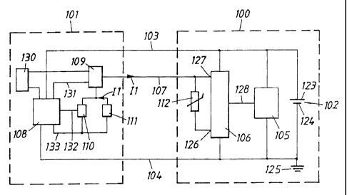
Figure 1 shows a schematic view ot an arrangement according
to the present invention, comprising a battery pack
attached to an electric device.
Figures 2a and 2b show schematic flow charts of a method
according to the present invention.
Figure 3 shows a schematic diagram of a relation between
temperature and resistance for a thermistor_
D'RT?3n=F'~ D$SC.RIPTION OF PREFERRF.D EMBODIMENTS
A first preferred embodiment of an arrangement according to
the present invention is shown schematically in figure 1. A
battery pack 100 is electrically and mechanically connected
to an electric device 101. The battery pack 100 and the
device 101 are schematically shown as boxes in order to
stress the fact that the present invention relates to a
CA 02340380 2001-02-08
WO 00/11774 PCT/SE99/01421
6
diverse collection of battery powered electrical
implements. I'or the same reason, the actual means for
mechanical and electrical connection !=lave been omitted from
the illustration. It is also to be understood that the
battery pack 100 and the device 101 are mechanically and
electrically attachable and detachable from each other.
A typical example of this kind of arrangement is a portable
mobile telephone terminal equipped with a detachable
battery pack.,However, it is to be understood that a person
skilled in the art is capable of implementing the present
invention in other types of batte=y powered devices without
applying any inventive efforts.
The battery pack 100 comprises a battery cell 102, or a
collection of cells, with a positive terminal. 123 and a
negative terminal 124. The negative terminal is designated
as being signal ground as indicated by the signal ground
symbol 125. A battery processor 105 and an input/output
(I/O) unit 106 is also comprised in the battery pack 100,
both of which are connected to the positive terminal 123 of
the battery cell 102 and signal ground 125. The battery
processor 105 is connected to thc I/O unit 106 via a first
signal connection 128. Although the connection 128 is
illustrated as a single lead, it is to be understood that
this is only for illustrative purposes, and hence any=form
of multi-lead data bus etc_ is feasible.
Within the battery processor 105 are means for performing
processing tasks ruled by software, as is known in the art_
Although not shown in the figure, means such as control
logic and memory, read-only as well as random access, are
comprised in the battery processor 105.
The I/O unit 106 has a number of terminals, of which only
two are illustrated in figure 1 in addition to 'the
CA 02340380 2001-02-08
WO 00111774 PC.~T/SE99/o1421
7
connections to the battery cell 102. A bi-directional port
127 and an out port 126.
A thermistor 112 is connected to both the bi-directional
port 127 and the out port 126. Since figure 1 is only a
schematic illustration of the arrangement accordi,ng to the
invention, the locations of the different parts of the
battery processor 105 with respect to each other are not to
be taken literally. For example, the thermistor 112 is
preferably located in physical contact with the battery
cell 102 in order to be sensitive to temperature changes in
the cell 102.
Figure 3 illustrates a typical resistance-temperature
(R(T)) relation 301. That is, for a given temperature T1
the corresponding resistance R1 is determined by the R(T)
relation.
The battery processor 105 is capable of, by means of
software running in its logic circuits, controlling signal
flow through the I/O unit 106. In particular, as it is a
prerequisite for the present invention, the battery
processor 105 performs the task of connecting and
disconnecting the bi-directional port 127 and the out port
126. In practical terms this may, within the I/0 unit 106,
be realized by switches, which connects the ports either to
a high impedancestate, or to a low impedance state, that
is to signal ground 125.
Needless to say, the circuitry in the battery pack 100 may
be physically located either in separate units, such as
illustrated in figure 1, or integrated into one single
unit.
The electric device 101 comprises a device processor 108
which is connected to the battery cell 102 in the battery
pack 100 via a supply lead 103 and a signal ground lead
CA 02340380 2001-02-08
WO 00/I I774 PCTISE99/01421
8
104. Connected to the device processor 108 are a number of
units, some of which are dedicated to the specific task of
the device 101, schematically illustrated by a single
device specific circuit block 130. One example of a device
specific block 130 is an input/output unit similar to the
Z/O-unit comprised in the battery pack 100. Such an
input/output unit may perform the task of mediating signal
sequences from the device processor 108 and the battery
processor 105 via the communication line 107. Zn fact, in
the present example such functionality of the device
specific block 130 is assumed_
However, the device block may also comprise, in the case of
a telephone terminal, a radio transceiver and all other
necessary telephone specific means as is well known in the
art.
The device processor 108 is further connected to a switch
109 via a switch control connection 131, an analog-to-
digital (A/D) converter 110 and a current generator 111 via
a common control connection 133. Both the A/D converter 110
and.the current generator 111 are also connected to the
switch 109. The A/D converter 110 generates digital output,
as is known in the art, and is connected via a data read
connection 132 to the device processor 108.
1
A communication line 107 is connected between the switch
107 and the bi-directional port 127 of the battery pack
100. As indicated above, it is outside the scope of the
present invention to specify any particular connection
means, such as electric and mechanical connectors, between
the device 101 and the battery pack 100_
Similar to the battery processor 105 in the battery pack
100, the device processor 108 comprises mans for performing
processing tasks ruled by software, as is known in the art.
Although not shown in the figure, means such as control
CA 02340380 2001-02-08
WO aD/I I774 PCT/SL99/0142I
9
logic and memory, read-only as well as random access, are
comprised in the device processor 108.
Software running in the device processor 108 controls the
switch 109 to the effect that the switch 109 can be in
either one of a first state and a second state. In the
first state the communication line 107 is connected to the
device specific circuits block 130 and disconnected from
the A/D-converter 110 and the current generator 111. In the
second state the communication line 107 is disconnected
from the device specific circuits block 130 and connected
to the A/D-converter 110 and the current generator 111.
A method of determining a temperature of the battery pack
100, which ideally corresponds to the temperature of the
battery cell 102, will now be described with reference to
flow charts illustrated in figures 2a and 2b. The
determination of the temperature is to be considered from
the point of view of the electric device 101. That is,
information representing the physical parameter temperature
is to be transferred from the battery pack 100 to the
device processor 108 of the device. As will be discussed
further below, a voltage level as measured across the
thermistor 112 is the information representing the
temperature of the battery pack 100.
All steps are considered to be realized by means of
software instructions running in the device processor 108
and the battery processor 105, and implemented in a manner
which is assumed to be within the grasp of a person skilled
in the art.
A more detailed description of how the information
regarding temperature is used or processed within the
device 101, after being determined by the inventive method,
is outside the scope of the present invention. Never-
theless, examples of how the temperature information may be
CA 02340380 2001-02-08
WO 00/11774 PCT/SE99/01421
used includc displaying ttie temperature to a user of the
device 101 as well as making use of the temperature when
controlling re-charging of the battery cell 102.
It is also to be noted that the method comprises a number
5 of sequential steps where information-carrying signals are
exchanged between the device processor 108 of the electric
device 101 arid the battery processor 105 of the battery
pack 100. The precise manner in which the software in the
processors 105,108 generates, transmits, receives and
10 interprets these signals, as well as the specific format of
the signals is assumed to be easily implemented by a person
skilled in the art. However, because of the simple fact
that a preferred embodiment of the present invEntion
comprises a single communication line 107 between the
battery pack 100 and the device 101, a serial communication
protocol is to be assumed.
Referring to figure 2a, the method commences with a
transmission step 202 performed in the device processor
108. A command representing an order to measure the
temperature of the battery pack 100 is transmitted from the
device processor 108, via the communication line 107, to
=..~
the battery processor 105.
Following the transmission step 210, the device processor
108 prepares to wait for the battery processor to perform
the steps described below in connection= with figure 2b,
including an acknowledgment of the order to measure the
temperature_ In a timer step 204 a timer (not shown) is
set, according to known technique, to trigger in a time-out
step 206 a time-out condition at a predetermined moment in
time as measured by an internal clock (not shown). The
duration ot time until this time-out is in this embodiment
predetermined in terms of a fixed time limit stored in the
device processor memory. The exact duration of the waiting
period is assurned to be such that the steps pertormed by
CA 02340380 2001-02-08
'wo 00/11774 PCT/SE99/01dZl
11
the battery processor 105, as described below, will be
satisfactorily executed.
When the preparation for the time-out is done in the timer
step 204, the device processor 108 receives an acknowled-
ging signal from the battery processor 105 that the
transmitted command has been successfully received in the
battery processor 105. The content of the acknowledging
signal is preferably in the form of an echo of the
temperature measurement command sent to the battery
processor 105 in step 202. This acknowledging echo is in
figure 2a illustrated in three steps, a reception step 208,
in which the acknowledging command is received, and an
interpretation step 210 where a check is made that the
command has been interpreted by the battery processor 105
as being the correct (temperature measurement) command. If
the echoed command is found to be incorrect, the method is
terminated, as indicated by a decision step 212, in which a
negative acknowledging command leads to an immediate
interruption of the method and a positive acknowledgment
leads to a continuation of the method.
Continuing now with steps performed in the battery
processor 105, it is illustrated in figure 2b a receiving
step 252. The battery processor 105 receives the command
transmitted via the communication line 107 from the device
processor 108. The exact path of the command, via the I/O
unit 106 to the battery processor 105 is considered to be
irrelevant in terms of explaining the invention and will
hence not be discussed further.
The received command is then interpreted in an
interpretation step 254. Depending on whether or not the
command is coded in any way or whether it is one of many
possible commands within a larger set of commands, this
interpretation may be more or less complicated- For the
purpose of this description, it is assumed that the command
CA 02340380 2001-02-08
WO 00/11774 PCT/SE99/01421
12
received is interpreted such that a result is obtained
which entails a positive identification of the order by the
device processor 108 to measure the temperature of the
battery pack 100.
As a consequence of the positive interpretation of the
order in the interpretation step 254, the battery processor
105 commences a procedure to enable a determination of the
battery temperature-
In a disconnection step 256, the battery processor 105
controls a switch (not shown) within the I/O unit 106 to
disconnect the communication line 107 from the I/0 unit
106. In practice this entails connecting the bi-directional
port 127 via an impedance unit (not shown), having a very
high impedance level, to signal gz'ound 125.
In a connection step 258 the battery processor 105 controls
a switch (not shown) within the I/O unit 106 to connect the
thermistor 112, via the I/O unit 106, to signal ground_ In
practice this entails connecting the out port 126 to signal
ground 125.
In an acknowledgment step 260, the received command to
measure the temperature is echoed back to the device
processor 108 in order to acknowledge that the battery
processor 105 has prepared the circuitry in the battery
pack for temperature measurement.
in order to enable for the device processor 108 to perform
the steps of measuring the temperature, the battery
processor 105 performs a sequence of waiting, as will be
described in the following steps. The duration of this
waiting is in this embodiment predetermined in terms of a
fixed time limit stored in the battery processor memory. In
a timer step 262 a timer (not shown) is set, according to
known technique, to trigger in a time-out step 264 a time-
CA 02340380 2001-02-08
WO 00/11774 PCT/SE99/01411
13
out condition at a predetermined moment in time as measured
by an internal clock (not shown) in the battery processor
105. The duration of time until this time-out, i.e, the
waiting period, is predetermined in terms of a fixed time
limit stored in the battery processor memory. The duration
of the waiting period is assumed to be such that the steps
performed by the device processor 108, described below,
will be satisfactorily executed_
Returning now to a description of steps performed in the
device processor 108, after the positive acknowledgment by
the battery processor 105 as described above in connection
with steps 260,208,210 and 212.
In a first switching step 214, the device processor 108
disconnects the device specific circuitry 130 from the
communication line 107 and connects both the A/D converter
110 and the current generator 111 to the communication line
107. In practice this step is performed in accordance with
known digital technique by the device processor 108 in that
it controls the switch 109 via the switch contro].
connection 131.
In a current generating step 216, the device processor 108
controls the current generator 111, via the common control
connection 133, to generate a predetermined constant
electric current I1. The current I1 flows via the switch
109 through the communication line 107 and through the
thermistor 112 and returns via the signal ground lead 104.
During the current generating step 216, the device
processor 108 also performs a voltage detection step 218.
The predetermined constant current 11 passing through the
thermistor 112 results in a voltage drop across the
thermistor. This voltage drop, having an analogue voltage
level V1, is detected by the A/D converter and is according
CA 02340380 2001-02-08
= WO 00/11774 aCT/SE99101021
14
to known art converted to a digital value which is read by
the device processor 108 via the data read connection 132.
Following the reading of the voltage level V1 in the
detection step 218, the device processor 108 performs a
calculation step 220. The software in the device processor
108 has access to the voltage level V1 as well as the
predetermined current level 11. In simple terms, the
calculation entails dividing the voltage level V1 with the
current level I1, which results in a resistance value R1
according to Ohm's law.
In an interpretation step 222 the device processor 108 then
performs an interpretation of the calculations made in the
calculation step 220. The resistance-temperature relation
R(T), illustrated in figure 3, is according to known art
stored in the processor 108 and used to extract the
temperature T1 corresponding to the resistance value R1.
Following the calculation and interpretation, the device
processor 108 disconnects the A/D converter 110 and the
current generator 111 from the communication line 107 and
reconnects the device specific circuitry 130 to the
communication line 107. In practice this is performed in a
second switching step 224 in the same manner as in the
first switching-step 214.
Returning now to steps performed by the battery processor
105, it is to be noted that the waiting period, as
discussed in connection with the waiting in steps 262 and
264 above, has lapsed.
In a disconnection step 266 the battery processor 105
controls the 1/O unit 106, via the connection 128, to
disconnect the thermistor 112 from signal ground 125, that
is reversing the connection step 258.
CA 02340380 2001-02-08
'wo 00/11774 PC'T/SE99/01421
To conclude the method, the battery processor lOS performs
a connection step 268 in which the bi-directional port 127.
is reconnected to the communication line 107, thus re-
enabling exchange of digital information between the
5 battery processor 105 and the device processor 108.