Note: Descriptions are shown in the official language in which they were submitted.
CA 02340488 2001-03-13
SWITCH MATRIX FOR SATELLITE PAYLOADS WITH IvIULTIPLE UPIINK
BEAMS AND ON-BOARD SIGNAL PROCESSING
BACQKGROUND OF TI M INVENTION
1. Field of the Invention.
This invention relates in general to switch matrices, and in particular to a
switch
matrix for satellite payloads with multiple uplink beams and on-board signal
processing.
2. Description of Related Art.
Communications satellites have become commonplace for use in manytypes of
communications services, e.g., data transfer, voice communications, television
spot beam
coverage, and other data transfer applications. As such, satellites must
provide signals to
various geographic locations on the Earth's surface. As such, typical
satellites use
customized antenna designs to provide signal coverage for a particular country
or
geographic area.
Many satellite payloads contain analog or digital signal processors. Analog
processors are typically used to separate and combine different signals into
specific
channels ("channelize the signals"), and to switch different parts of the
ground-to-
satellite ("uplink") signal to different satellite-to-ground ("downlink")
beams. Digital
processors are also used to channelize and switch signals, and may also be
used to
demodulate, process and remodulate signals. Usually these signal processors
are heavy
and consume a lot of DC power, so it is advantageous to be as efficient as
possible in
allocating processing resources to uplink beams.
CA 02340488 2001-03-13
-2-
Typically, the signals ("traffic") in each uplink beam to the satellite are
different,
since the population and economy in each uplink region is different. If the
amount of
traffic in each uplink beam is known before the satellite is launched, and
does not vary
over the life of the satellite, processing resources can be allocated to
uplink beams with
fixed connections, which eliminates the need for the switch matrix. Typically,
however,
the amount of traffic in each uplink beam is either unknown beforehand or
varies over
time, and thus there must be some sort of switch matrix to reallocate and
interconnect
uplink beams to the on-board satellite processing resources.
Some. traditional switch matrix designs, such as the crossbar switch or the
C1os
switch n-iatrix, were designed for use in telephone switching networks, and
are designed
for point-to-point connectivity. Other switch matrices have been designed for
connections inside a computer or between networked computers. Some of these
designs
are not suitable for satellite signals at microwave frequencies, because the
related art
switch matrix designs suffer from isolation problems at microwave frequencies.
Other
switch matrices do not provide for point-to-multipoint connectivity without
excessive
signal losses caused by power splitting. Many designs are also difficult to
build out of
smaller pieces_ in a modular manner.
It can be seen, then, that there is a need in the art for a switch matrix that
is
suitable for use in a spacecraft environment. It can also be seen that there
is a need in
the art for a switch matrix that provides point-to-multipoint connectivity
without
excessive signal losses. It can also be seen that there is a need in the art
for a switch
matrix that provides ease of mechanical design and construction to reduce
spacecraft
costs.
CA 02340488 2004-05-10
3
SUMMARY OF THE INVENTION
To overcome the limitations in the prior art described above, and to overcome
other limitations that will become apparent upon reading and understanding the
present
specification, the present invention discloses a method and apparatus for
switching signals
through a switch matrix. The apparatus comprises an input module and an output
module.
The input module has a plurality of inputs typically equal to a number of
cells in a reuse
pattern, and the inputs receiving at least one uplink beam. The input module
also has a
plurality of outputs, the plurality of outputs is typically equal to the
number of subbands in
the uplink beam. The output module is coupled to the input module and
selectively
couples the outputs from the input module to an output of the output module
that is
coupled to a demodulator.
The method comprises the steps of grouping the uplink signals into a plurality
of
groups, the number of uplink signals typically equal to the number of cells in
a cell-based
transmission matrix and the number of groups at least equal to a number of
cells in a reuse
pattern in the cell-based transmission matrix, where each group comprises a
signal from
each frequency used in the frequency reuse pattern. Each group of uplink
signals is then
separated into subband signals, which are then grouped together into groups of
similar
subband signals. The groups of similar subband signals are then forwarded to
demodulators for processing within the satellite system.
The present invention provides a switch matrix that is suitable for use in a
spacecraft environment. The present invention also provides a switch matrix
that provides
point-to-multipoint connectivity without excessive signal losses. The present
invention
also provides a switch matrix that provides ease of mechanical design and
construction to
reduce spacecraft costs.
According to another aspect of the present invention, there is provided a
switch
matrix for coupling an uplink beam to a demodulator in a satellite system,
wherein the
satellite system receives input from cells in a cell pattern, comprising: (a)
a plurality of
input modules, each having a plurality of inputs at least equal to a number of
cells in a
reuse pattern for the satellite system, each input module comprising: (1) a
plurality of
power splitters, wherein the plurality of power splitters is at least equal to
the number of
cells in the reuse pattern for the satellite system, wherein each power
splitter splits each
CA 02340488 2004-05-10
3a
input into a plurality of substantially equal power outputs, a number of power
outputs at
least equal to a number of subbands used by the satellite system; and (2) a
plurality of
switch modules, coupled to the plurality of power splitters, each switch
module accepting
a plurality of inputs at least equal to the number of cells in the reuse
pattern for the
satellite system, the plurality of switch modules at least equal to the number
of subbands
used by the satellite system; and (b) a plurality of output modules, coupled
to the input
modules through the plurality of the switch modules, each having a plurality
of inputs at
least equal to the number of cells in the cell pattern, comprising: (1) a
first set of output
matrices, each output matrix in the first set of output matrices having a
plurality of inputs
at least equal to the number of subbands used by the satellite system; and (2)
a second set
of output matrices, coupled to the first set of output matrices, each output
matrix in the
second set of output matrices having a plurality of outputs at least equal to
a number of
demodulators used by the satellite system in each subband.
CA 02340488 2001-03-13
-4-
BRIEF DESCRIPTION OF THE DRAWINGS
Referring now to the drawings in which like reference numbets represent
corresponding parts throughout:
FIG. 1 illustrates an exemplary block diagram of the uplink of a satellite
with
digital processing;
FIG. 2 illustrates the switch matrix of the present invention;
FIG. 3 illustrates the structure of the input switch modules of the present
invention;
FIG. 4 illustrates an output switch modttle in accordance with the present
invention;
FIG. 5 illustrates a switch matrix in accordance with the present invention
that is
used in dual-polarized uplink configurations;
FIG. 6 illustrates a switch matrix in accordance with the present invention
that is
used in dual-polarized uplink configurations with varying polarizations within
an uplink
bean-4
FIG. 7 illustrates a switch matrix in accordance with the present invention
that
can use multiple polarizations simultaneously,
FIG. 8 illustrates a single input module with redundant input connections in
accordance with the pc-esent invention;
FIG. 9 illustrates a specific example of a redundant input matrix of the
present
invention;
FIG. 10 illustrates a design that provides redundancy in the downconverters
and
in the input switch module of the present invention;
CA 02340488 2001-03-13
-5-
FIGS. 11 and 12 illustrate examples of failures within the configuration of
FIG.
10;
FIG. 13 illustrates a complete design of a switch matrix of the present
invention;
FIGS. 14A- 14B illustrate the packaging of the present invention compared to
the
related art; and
FIG. 15 is a flow chart illustrating the steps used to practice the present
invention.
CA 02340488 2001-03-13
-6-
DETAILED DESCRIPTTON OF THE PREFERRED EMBODIMENT
In the following description of the prefen-ed embodiment, reference is made to
the
accompanying drawings which form a part hereof, and in which is shown byway of
illustration a specific embodiment in which the invention may be practiced. It
is to be
understood that other embodiments may be utilized and structural changes may
be made
without departing from the scope of the present invention.
Overview Of Related Art
Switch matrices are commonly used in many satellite telecommunications
systems designs to allow for redeployment of signals onboard the satellite.
The switch
matrix allows an input signal to be routed to any output desired througli the
use of
crossbar switches or other types of switch matrices.
Some traditional switch matrix designs, such as the crossbar switch or the
Clos
switch matrix, were designed primarily for telephone switching networks, and
are
designed for point-to-point connectivity. Other switch matrices were designed
for
connections inside a computer or between networked computers. Some of these
designs
are not suitable for microwave signals because of isolation problen-is, and
other matrices
do not provide for point-to-rnultipoint connectivity without excessive losses
due to
power splitting. Many designs are not easy to build out of smaller pieces in a
modular
manner.
The present invention is suitable for microwave work, provides for point-to-
multipoint connectivity with a greatly reduced amount of power splitting, and
can be
constructed from smaller pieces in a modular manner.
CA 02340488 2001-03-13
-7-
FIG. 1 illustrates an exemplary block diagram of the uplink of a satellite
with
digital processing.
The system 100 comprises an uplink antenna 102, downconverters 104, switch
matrix 106, demodulators 108, and a digital signal processor (DSP) 110. Uplink
antenna
102 receives a number of uplink beams 112, in this case 128 uplink beams 112,
which are
each fed to individual downconverters 104. Each downconverted uplink signal
114 is
input to the switch matrix 106, which routes each signal to a given output of
the switch
matrix 106. The output signals 116 of the switch matrix are fed into
demodulators 108,
and then input to DSP 110 for processing. The DSP 110 has the capacity to
service a
plurality of demodulators 108.
The system 100 is usually employed in a satellite telecommunications system
that
receives uplink information from transmitters on the ground. These
transmitters are
assigned in a"cellular" pattern, where each cell transmits information to the
satellite
within a given frequency band. Each cellwithin a frequency reuse group of
cells uses a
different frequency band, and such groups are repeated throughout the cellular
pattern to
create a frequency-reuse pattern within the totality of cells in the system.
Within each
cell, the frequency band is divided into subbands. Each subband comprises
individual
signals from subscriber units, and each subband can contain zero or more
signals.
For example, in FIG. 1, each demodulator 108 demodulates one of eight uplink
subbands. If the traffic is uniforni, each uplink beam 112 will be allocated 2
demodulators 108, and each uplink beam 112 can carry 1/4 of its maximum
capacity. In
such a case, each uplink beam 112 can be hardwired to two demodulators 108
directly
CA 02340488 2001-03-13
-8-
without using switch matrix 106, etc. until all 128 uplink beams 112 are
connected to
demodulators 108.
Typically, however, the traffic is not uniform, and each uplink beam 112 will
carry a different amount of traffic, which makes switch n-iatrix 106 a
necessary part of
system 100. Further, the traffic distribution changes during the lifetime of
the satellite,
possibly changing every hour or so. Switch matrix 106 is used to dynan-ucally
allocate
demodulators 108 to uplink beams 112. In the example of FIG. 1, a switch
matrix 106
with 128 inputs and 256 outputs is needed.
The most straightforward design for the switch matrix 106 of FIG. 1 is a
crossbar
switch in which every input 114 can be connected to any output 116 in any
order, with
each signal passing through one switch in the switch matrix 106. However, such
a large
crossbar switch matrix 106 would require 128''256 = 32,768 switches, and would
be very
difficult to manufacture in a modular manner from smaller switches.
The number of switches in switch matrix 106 can be somewhat reduced by using
architectures like the Clos architecture, but the resulting matrix would still
be difficult to
manufacture in a modular manner. Crossbar and C1os design switch matrices 106
are not
suitable for the system 100 of FIG. 1, either because they are not suitable
for microwave
switching networks due to isolation and connectivity problems, or because they
cannot
satisfy the point-to-multipoiuit requirements for system 100.
To broadcast one uplink signal 114 to multiple outputs 116, a power splitter
is
required inside of switch matrix 106. The more the uplink signal 114 is split,
the greater
the power loss through the switch matrix 106. In power limited applications
such as
spacecraft, it is vitally important to reduce this power loss as much as
possible to reduce
CA 02340488 2001-03-13
-9-
the need for amplifiers within the system 100, to reduce both power
consumption and
weight on board the satellite.
For the switch matrix 106 described in FIG. 1, one uplink signal 114 must have
the capability to be broadcast to 8 of the 256 outputs 116. This capability is
typically
provided by using a 1:256 power divider, followed by a switching network,
within switch
matrix 106. For satellite applications, this approach leads to unacceptably
high losses
within the switch matrix 106.
However, switch matrices 106 of the related art were not optimized to take
into
account how system 100 is typically implemented. First, satellite payioads
with multiple
uplink beams 112 typically use a frequency reuse scheme such as 4-cell or 7-
cell
frequency reuse. Adjacent cells within the frequency reuse scheme cannot use
the same
frequency and, therefore, cannot use the same subbands. This reduces the
connectivity
requirements of the switch matrix 106, as described herein with respect to the
present
invention. Second, the demodulators 108 may often be grouped by subband, e.g.,
some
demodulators 108 demodulate only the fiust subband, other demodulators 108
only the
second subband, etc. One input signal 114 must have the capability to be
broadcast to
all of the different subband demodulator 108 types, but one input signal 114
does not
have to be broadcast to more than one demodulator 108 in a given group of
demodulators. As such, the switch n-iatrix of the present invention is further
reduced in
complexity while still providing the interconnections required for system 100.
CA 02340488 2001-03-13
-10-
Overview Of The Invention
The invention allows for a flexible allocation of processing resources to
uplink
beams for satellite payloads with on-board processing, which allows the
processor
resources to be used more efficiently. This reduction on the coniplexityof the
switch
matrix reduces the weight and power required by the processor to accomplish
the
mission goal. The present invention is simpler than comparable switch matrices
and can
be constructed from simpler switches allowing it to be used for satellite
payioads. The
amount of power splitting inside the switch matrix of the present invention is
reduced, so
it has a lower loss and a lower noise figure than other related art designs.
This invention applies to all satellites with digital or analog processing of
signals
that divide multiple uplink signals into several subbands. It is most useful
when the
uplink traffic distribution varies over time or is not well known before
launch.
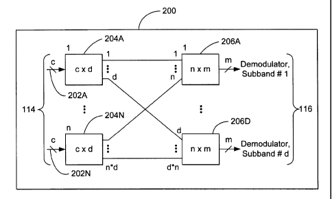
FIG. 2 illustrates the switch matrix of the present invention. A satellite
using
switch matrix 200 of the present invention uses multiple uplink beams 114 that
use c-cell
frequency reuse, where c is the number of cells in the reuse pattern. Input
signals 202A
are therefore input to input switch module 204A, and input signals 202A
comprise c
uplink beams,_ which equals one entire reuse pattern. C is typically equal to
3, 4, 7, 9, or
12, but can be other numbers. N is the number of reuse patterns on the ground.
As
such, the total number of uplink beams 114 is c tirnes n(c',n). To accommodate
the
entire complement of uplink beams 114, n input switch modules 204A-204N are
used to
receive all of the c'''n uplink beams 114.
The uplink signals 114 are mulitcarrier, and to accomplish the demodulation,
the
uplink signal 114 is divided into d subbands. Therefore, each input switch
module 204A-
CA 02340488 2001-03-13
-11-
204N must provide d outputs. The output switch modules 206A-206D must accept
one
input from each input switch module 204A-204N, and therefore have n inputs. A
demodulator 108 can demodulate one of these d subbands, and m demodulators are
devoted to each subband. The total number of demodulators 108 is therefore &m,
and
each output switch module 206A-206D must provide m output signals. Therefore,
each
output switch module is an n'rm matrix.
Switch matrix 200 of the present invention comprises n input switch modules
204A-204N, and d output switch modules 206A-206D. Each of the inputs 202A to
the
input switch module 204A comes from a single uplink reuse group, so that none
of the
inputs 202A can share an uplink frequency. The switch matrix 200 of the
present
invention thus has a c~-m input capability, and a d' m output capability,
which provides
proper interconnectivity for the system 100 witliout excess weight or power
consumption.
InPut Switch Modules
FIG. 3 illustrates the structure of the input switch modules of the present
invention. Each input switch module 204A-204N receives inputs 202A-202N. For
clarity, input switch module 204A is shown as a typical design. Signals 202A,
which
comprise signals 300 and 302, are fed into a plurality, i.e., "c" 1-to-d power
splitters
304A-304C Eacli power splitter 304A-304C takes a suigle input signal, e.g.,
300, and
produces a plurality of substantially equivalent power outputs from signal
300, e.g.,
306A-306D. For example, if power splitter 304A was a 1:4 power splitter, and a
100
nucrowatt ( W) input signal 300 was fed into power splitter 304A, then power
splitter
CA 02340488 2001-03-13 -
-12-
304A would produce four output signals 306A-306D, each approxiniately a 25 W
signal. There would be some losses through power splitter 306A, which would
reduce
the 25mW output power of each signal by some percentage amount. In the related
art, a
similar input signal would be split 256 times, making cach output signal less
than l W,
which may be difficult to process without amplification.
Each output 306A-306D from each power splitter 304A-304C is fed into a c:1
switch 308A-308D. Since each switch 308A-308D produces only one output 310A-
310D, there are d switches 308A-308D in each module 204.
Output Switch Modules
FIG. 4 illustrates an exemplary output switch module in accordance with the
present invention. Output switch module 206A, shown as a typical output switch
module 206, is a concentrator, e.g., output switch module 206A receives the n
input
signals 310 from the input modules 204 and allows only m of the n input
signals 310 to
be output signals 116 from output switch module 206A. Every output 116 of an
output
switch module 206A is connected to a demodulator 108 that demodulates one of
the d
subbands. Since each output 116 is identical, the output switch module 206A
does not
have to be fully connected as in the related art, but the output switch module
206A
should ensure that in any arrangement of inputs 310, the subset of inputs 310
must be
switchable to an output 116. Since each group of c cells cannot use more than
d
demodulators, m, which is the number of demodulators of one type, must be less
than or
equal to n, the number of frequency reuse groups.
CA 02340488 2001-03-13
-13-
The complexity of the output switch modules 206 may vaiy greatly with n and m.
For example, if m= n, then the output switch modules 206 become straight
connections
from input 310 to output 116 with no switching required. However, If n is the
square of
a number, it is possible to build the output module from simpler submodules.
As an
example shown in FIG. 4, if input signals 310 number 64 and the output signals
116
number 32, it is possible to build the output switch module 206 using eight 8
x 8 input
submodules 400A-400H and eight 8 x 4 output submodules 402A-402H. Since all of
the
outputs of the output module 206 are identical, the output module does not
have to be
fullyconnected, which allows the present invention to implement a switching
scheme
that is simpler than a crossbar architecture for the output module 206.
However, the
output switch module 206A as shown is fully connected, which allows for any
traffic
pattern on the ground that is supported by frequency reuse rules and by the
capacity of
the processor to be supported by the output switch module 206. This way, if
the traffic
distribution changes during the life of the satellite, the switch matrix can
be reconfigured
to support the new traffic distribution.
Constructing the output switch matrix 206 out of simpler submodules 400 and
402 makes it easier to manufacture and test the design of the present
invention over that
of a full crossbar switch. Modules can be produced and tested separately from
the rest,
and the production of numerous identical modules can make product design
easier.
In the discussion above, it is assumed that the outputs of each output
submodule
402A-402H are connected to different types of demodulators with each type
demodulating a different subband. The output switch module 206, however, can
be used
CA 02340488 2001-03-13
-14-
with any payload that has multiple uplink beams with frequency reuse and has
some sort
of processing, analog or digital, that splits the uplink band into several
subbands.
Alternative Embodiments of the Present Invention
FIG. 5 illustrates a switch matrix in accordance with the present invention
that is
used in dual-polarized uplink configurations. Satellite systems often use a
dual polarized
uplink, with some signals transmitted up with right-hand circularly polarized
(RHCP)
carriers with the others using left-hand circularly polarized (LHCP) carriers.
In some
systems, users in a particular uplink beam are constrained to use only one
polarization, so
that half of the uplink beams use RHCP and the other half of the uplink beams
use
LHQ'.
As shown in FIG. 5, system 500 divides the uplink beams 114 in half. One-half
of the uplink beams 114 in a reuse group will be LHCP, and are grouped in one
input
module 502A, while the other input beams are RHCP and are grouped in a
separate
input module 502B. The resultant system 500 has twice the number of input
modules
502A-502B as system 200, but each input module 502A-502B has one-half the
number
of inputs as input modules 204A-204N.
Since both polarizations are used in system 500, the maximum capacity of the
spacecraft is doubled which means twice the number of demodulators 108 can be
employed by the spacecraft. As such, m, the number of demodulators, may be as
large as
2n, the number of reuse patterns on the ground, since every reuse pattern may
use both
polarizations. Therefore, the output switch modules 504A-504B should contain
inputs
numbering 2n, and outputs numbering m.
CA 02340488 2001-03-13
-15-
FIG. 5 illustrates the case where the number of uplink bearns 114 is even.
However, the number of uplink beams 114 can be an odd number, thereby making
exact
division by two impossible. If the number of uplink beams 114 is an odd
number, the
c/2 input beams 506 number (c +1)/2, and the number of inputs 508 to the
output
switch modules 504A-504B number 2c~rn/(c+1).
FIG. 6 illustrates a switch matrix in accordance with the present invention
that is
used in dual-polarized uplink configurations with varying polarizations within
an uplink
beam. As discuss with respect to FIG. 5, some satellite systems use polarized
uplink
beams. FIG. 5 illustrated the scenario that described users in a particular
uplink beam
that are constrained to use only one polarization. The scenario of FIG. 5 was
limited to
a fixed polarization for each uplink beam, but this polarization may change
over the life
of the satellite. FIG. 6 illustrates a switch matrix that can be used in such
a scenario.
System 600 utiliz,es an input signal 114 from every cell c in the reuse group,
but
doubles the number of outputs from each input switch module 602A-602N to twice
the
number of bandwidths, i.e., 2d. To accommodate the increased number of outputs
from
input switch modules 602A-602N, the number of inputs 604 to each output switch
module 606A-606D is increased to twice the number of the reuse patterns on the
ground, or 2n. As with FIG. 5, since both polarizations are used, the maximum
capacity
of the spacecraft is doubled, so that the number of demodulators 108, or m,
can be as
large as 2n. However, in system 600, each input switch module 602 has two
outputs
608A-608D that are coupled to an output switch module 606A-606D, e.g., input
switch
module 602A has two outputs 608A coupled to inputs 604 numbers 1 and 2 on
output
switch module 606A. System 600 can also be used to provide redundancy within
the
CA 02340488 2001-03-13
-16-
system, for example, if output 1 of input switch module 602A were to fail,
output 2 can
still connect input switch module 602A to output switch module 606A.
FIG. 7 illustrates a switch matrix in accordance with the present invention
that
can use multiple polarizations simultaneously. System 700 illustrates a system
that uses
an uplink antenna with two output ports per beam, one for each polarization.
This use
of two output ports doubles the number of antenna outputs, which doubles the
number
of inputs 114 to the number of inputs to the switch matrix 700. The number of
input
switch modules 702A-702N has doubled to 2n, one input switch module 702A-702N
for
each cell group. As with FIGS. 5 and 6, the maximum capacity of the spacecraft
is
doubled since both polarizations are used, and therefore, the number of
demodulators
maybe as large as twice the number of cell patterns on the ground, which
forces the
number of inputs to the output switch modules 704A-704D to be 2n and the
number of
outputs to be m, where m may be as large as 2n.
Redundancy Designs
The designs of FIGS. 2-7 are all somewhat vulnerable to single point failures.
However, redundancy can be designed into a switch matrix of the present
invention to
avoid single point failures within the spacecraft. For example, if a switch on
an output
port of an output module 206A fails, the demodulator 108 that follows the
switch is no
longer useable, because the demodulator 108 will no longer receive an input.
For this
reason, additional demodulators 108 in each subband can be installed to allow
a signal to
be rerouted through the switch matrix of the present invention for that
subband.
CA 02340488 2001-03-13
-17-
The present invention can also have redundancy built in to avoid single point
failures within the matrix itself. For example, referrring to FIG. 2, there
are n''d
interconnections between the input switch modules 204A-204N and the output
switch
modules 206A-206D. Since there are only md outputs 116, and m<n, some of the
interconnections between input switch modules 204A-204N and output switch
modules
206A-206D have no usable signals going through them. If some of the switches
are lost
on either side of these uiterconnections, which would render those switches
unusable,
the impact to the system is typically not very large.
On the other hand, the loss of an input port to the switch matrix is very
serious.
Referring again to FIG. 2, if one of the input ports receiving uplink beams
114 is not
useable, the uplink beam 114 connected to that port is also unusable. This
leads to a
hole in the coverage of the satellite where terminals can not uplink to the
satellite.
Although the input port is connected to a 1:c power splitter, and this passive
device
typicallydoes not fail nearly as much as an active switch, the small chance of
failure is
often unacceptable. In these cases, the input module can be redesigned to make
it more
redundant.
FIG. 8 illustrates a single input module with redundant input connections in
accordance with the present invention.
Typically, the input to the switch matrix includes a downconverter 104 as
shown
in FIG. 1. The input redundancy for the switch matrix can be combined with the
downconverter 104 redundancy. For example, uplink cells 112, instead of being
input
directly into downconverters 104, are input to a redundancy matrix 800.
Redundancy
matrix can be used to supply any level of redundancy, but for ease of
explanation, a c+1
CA 02340488 2001-03-13
-18-
for c redundancy is described herein. For example, since there are c cells in
a reuse
group, one additional output is provided from each redundancy matrix 800 to
prevent a
failure of an input port on input switch module 204A from being a single point
failure
for a given uplink beam 112. This provides inputs 802A to 802N to input switch
module
204A, which is now a (c + 1) x d matrix. It can be seen that additional
redundancy or
alternative redundancy schemes can be provided by making redundancy matrix 800
a
c +n for c matrix, and input switch module a (c +n) x d matrix.
FIG. 9 illustrates another example of a redundant input matrix of the present
invention, related to the embodiment of FIG. 5. Input beams 112 for a four
cell reuse
system having a fixed polarization per cell will use 4 inputs to redundancy
matrix 801,
which provides an eight-for-seven redundancy. Redundancy matrix 801 will
produce
eight outputs for a single polarization, namely 802A through 802H. Each output
802A
through 802H is provided to input switch module 204A, and modules 304A through
304D respectively. There are a total of eight subbands, and therefore modules
304A
through 304D produce 8 outputs. The downconverter 104 redundancy is 8 for 7 as
are
the inputs to input switch module 204A.
Redundancy matrix 800 also provides redundancy for each uplink beam 112. If
an input to input switch module 204A fails, for example input 802A, uplink
beam 112
number 1 can be rerouted to input 802B, which can then switch uplink beam 112
number 1 through input switch module 204A and module 304A. This is done by
using
hybrid 900 and hybrid 902, which can route the uplink beam 112 to either input
802A or
802B. Siniilar results can be achieved for all of the uplink beams 112.
CA 02340488 2001-03-13
-19-
Depending on how the downconverters 104 are configured, the signal from
uplink beam 112 number 3 can be paired with the signal from uplink beam 112
number
2 or the signal from uplink beam number 4. Therefore, uplink bearns 112 2, 3,
and 4
should all have the same polarization assignment, and uplink beam 112 number 3
should
originate from a cell that cannot share frequencies with uplink beam number 2
or uplink
beam 112 number 4. Preferably, all of the uplink beams 112 assigned to the
redundancy
matrix 800 should have the same polarization assignments, and uplink beams 112
assigned to adjacent inputs should originate from cells that cannot share
frequencies
because they are in the same cell frequency reuse pattern.
While the design in FIG. 9 provides some redundancy in the downconverters 104
and input switch module 204A inputs, the design of FIG. 9 does not allow for
two
downconverters 104 in a single redundancy matrix 800 to fail, nor does it
provide
provide any redundancy for the input modules 304A-304D of the input switch
module
204A.
FIG. 10 illustrates a design that provides redundancy in the downconverters
and
in the input switch module of the present invention.
System 1000 comprises two redundancy mattices 800. Within each redundancy
matrix 800, each uplink beam 112 is input to a hybrid power splitter 900,
which has
outputs to two different downconverters 104. This configuration makes
downconverters
104 fully 2 for 1 redundant, so that more than one downconverter can fail in a
single
redundancy matrix 800.
CA 02340488 2001-03-13
-20-
Each uplink beam 112 is also sent to two different power splitter modules 304A-
304H within input switch module 204A. For example the primary output for
uplink
beam 112 1002 is sent to an input on module 304A, while the redundant output
for
uplink beam 112 1004 is sent to an input on a different module 304B. With the
configuration of FIG. 10, the input switch module 204A can survive the failure
of 1
input module 304A-304I-I. As with FIG. 9, uplink beams 112 should be paired
such that
adjacent inputs should come from cells that have the same polarization
assignment and
are within the cell frequency reuse pattern.
FIGS. 11 and 12 illustrate examples of failures within the configuration of
FIG.
10. As shown in FIG. 11, the downconverter 104P, the primary downconverter 104
for
uplink beam 112 number 11 has failed. The spacecraft, either through
autonomous
operation, monitoring of the downconverter 104P, or manual 'uitervention, can
switch to
redundant downconverter 104R Input 1100 to module 304G will no longer receive
inputs from downconverter 104P. However, uplink beam 112 number 11 can still
be
switched through input switch module 204A through input 1102 to module 304F.
Other
uplink beams 112 may also have to be switched through the input switch module
204A
to prevent interference. For example, uplink beam 112 number 9 is typically
not within a
four cell reuse pattern with uplink beam 112 number 11, so uplink beam 112
number 9 is
also switched to the redundant downconverter 104R associated with uplink beam
112
number 9. Input 1104 no longer receives input from uplink beam 112 number 9,
which
is switched through input switch module 204A through input 1105 on module
304E, and
is paired with uplink beam 112 number 8. If the traffic densiry is low and if
there is no
need for uplink beam 112 number 9 to use the same subband as uplink beam 112
CA 02340488 2001-03-13
-21-
number 11, uplink beam 112 number 9 can continue on input 1104 through primary
downconverter 104P until primary downconverter 104P fails, or the traffic in
the region
becomes heavy enough that uplink beam 112 number 9 and uplink beam 112 number
11
must use the same subband.
FIG. 12 illustrates an example where a module 304 in input switch module 204A
fails. If module 304B fails, all of the inputs to module 304B become unusable
byinput
switch module 204A. The primary inputs 1200 and 1202 are associated with
uplink
beam 112 number 3 and uplink beam 112 number 4, which must be switched to
redundant inputs 1204 and 1206, respectively.
Other switching may have to take place within input switch module 204A to
maintain correct uplink beam 112 pairings. For example, uplink beams 112
numbers 5,
6, and 7 may also require switching to inputs 1208-1212 respectively to
maintain proper
pairing or traffic density. If the traffic densityis low enough, some of the
uplink beanis
112 numbers 5, 6, and 7 may be kept with the associated primary downconverter
104,
but whenever there are three active inputs on a single module 304 the ability
of the
payload to concentrate capacity on the associated cells may be impaired.
FIG. 13 illustrates a complete design of a switch matrix of the present
invention.
For a four-cell reuse pattern with two polarizations, where each cell uses
only one of the
polarizations, the system 1300 of FIG. 13 can be employed. The design uses a
total of
112 uplink cells, so there are 112 uplink beams 112 going into the
downconverters 104.
The downconverters 104 are 2 for 1 redundant, and the primary and redundant
downconvertecs 104 have separate connections to the switch matrix, for a total
of 224
connections. The input modules 304 have four inputs and eight outputs, and are
CA 02340488 2001-03-13
-22-
connected to the downconverters 104 as shown in FIG. 10. The uplink bandwidth
is
broken into eight subbands, so there are eight different types of demodulators
108.
There are thirty-two demodulators 108 used for each subband, although a
smaller
number, for example twenty-eight demodulators 108, are typically needed to
meet
capacity specifications. The extra four demodulators 108 in each subband can
be used
for redundancy.
Packaeine
FIGS. 14A-14B illustrate the packaging of the present invention compared to
the
related art.
FIG. 14A illustrates a packaging scheme for the switch niatrix of the present
invention. Switch matrix 1400 consists of an input matrix 1402, an interface
plate 1404,
and an output matrix 1406. The input matrix has a number of "slices" 1408,
each
containing input modules 1410. Output matrix 1406 contains interconnect
rnatrices
1412 and output modules 1414, and consists of a plurality of "slices" each
containing
interconnect matnces 1412 and output modules 1414. The input modules 1410 are
connected to interconnect matrices 1412 through the interface plate 1404. As
such,
there are a large number of signals that must pass through interface plate
1404 to
connect input modules 1410 to interconnect matnces 1412 properly.
FIG. 14B illustrates an altemative packaging design illustrating a simpler
packaging design for switch matrix 1416 of the present invention. Switch
matrix 1416
comprises input modules 1408 directly coupled to output modules 1414, without
the
need for interface plate 1404 or interconnect matrices 1412. This reduces the
signal
CA 02340488 2001-03-13
-23-
density, and therefore the complexity of switch matrix 1416, making switch
matrix 1416
of the present invention easier to manufacture, test, and integrate into the
spacecraft.
However, switch matrix 1416 is not a fully connected matrix as the packagiiig
design of
FIG. 14A is. The switch matrix 1416 is thus less capable of in-flight
redistribution of
signals, because the beams are grouped into specific sections, and cannot be
switched
between one section and another. However, manyapplications may not require a
fully
connected matrix, and therefore, the packaging of FIG. 14B can be used to
simplify the
manufacture, testing, and integration of switch matrix 1416 into the
spacecraft.
Process Chart
FIG. 15 is a flow chart illustrating the steps used to practice the present
invention.
Block 1500 illustrates perfornung the step of grouping the uplink signals into
a
plurality of groups, the number of groups at least equal to a number of cells
in the cell-
based transmission matrix, each group comprising a signal from each frequency
used in the
frequency reuse pattern.
Block.1502 illustrates performing the step of separating each group of uplink
signals into subband signals.
Block 1504 illustrates performing the step of grouping similar subband signals
from the groups of uplink signals to produce groups of similar subband
signals.
Block 1506 illustrates performing the step of forwarding the groups of similar
subband signals to demodulators for processing within the satellite system.
CA 02340488 2001-03-13
-24-
Conclusion
This concludes the description of the preferred embodiment of the invention.
The
following paragraphs describe some alternative methods of accomplishing the
same
objects. The present invention, although described with respect to RF and
electrical
systems, can also be used with optical systems to accomplish the same goals.
Further, the
switches in the switch matrix can be actual switches, or hybrid electronics,
or other
switching mechanisms that perform similar functions.
In summary, the present invention discloses a method and apparatus for
switching
signals through a switch matrix. The apparatus comprises an input module and
an output
module. The input module has a plurality of inputs typically equal to a number
of cells in a
reuse pattem, and the inputs receiving at least one uplink beam. The input
module also has
a plurality of outputs, the plurality of outputs is typically equal to the
number of subbands
in the uplink beam. The output module is coupled to the input module and
selectively
couples the outputs from the input module to an output of the output inodule.
The method comprises the steps of grouping the uplink signals into a plurality
of
groups, the number of groups typicallyequal to a number of cells in the cell-
based
transmission matrix, where each group comprises a signal from each frequency
used in the
frequency reuse pattem. Each group of uplink signals is then separated into
subband
signals, which are then grouped together into groups of similar subband
signals. The
groups of similar subband signals are then forwarded to demodulators for
processing
within the satellite system.
The foregoing description of the preferred embodiment of the invention has
been
presented for the purposes of illustration and description. It is not intended
to be
CA 02340488 2001-03-13
-25-
exhaustive or to limit the invention to the precise form disclosed. Many
modifications and variations are possible in light of the above teaching. It
is intended
that the scope of the invention be limited not by this detailed description,
but rather by the
claims appended hereto.