Note: Descriptions are shown in the official language in which they were submitted.
CA 02340572 2001-03-13
NIETHOD AND APPARATUS FOR TESTING IMAGE SENSING CIRCUIT
ARR-kYS
Field of the Invention
The invention relates generally to image sensing circuits arravs, and more
particularly to the method and apparatus for testing the arrays.
Background of the Invention
A conventional sensing array is composed of individual light sensitive
circuits
called pixels that are organized in rows and columns. A row of pi:cels has a
common line
connecting the control gates of their respective access transistors. Data is
passed from
a pixel through its access transistor to a data line. Each column of pixels is
connected to
a common data line. During the manufacture of a sensor array, open or short
circuits may
occur between adjacent row lines or adjacent data lines due to the presence of
dust or
other particulate matter. Open or short circuiting of row lines or data lines
may also
occur due to improper control of the etching process.
CMOS image sensor arrays can employ several types of pixels. Passive pixel
sensor circuits are comprised of a simple photodiode and an access transistor.
Active
pixel sensor (APS) circuits have added features including a reset transistor
and a source
follower amplifier. Individual sensor circuits may suffer from similar
problems as the
row lines and data lines, in that they may be either short circuited or open
circuited and
therefore do not perform their proper function. In order to overcome these
problems,
defects in the sensor array must be detected in order to select arrays that
are acceptable
for use.
Integrated image sensors have traditionally been relatively expensive devices,
1.7
many of which used a technology known as charge coupled device (CCD). The
nature
of these devices did not permit the use of extensive integrated test features,
therefore
testing was primarily dependent on the use of external light sources. This
traditional test
CA 02340572 2001-03-13
7
method continued for the testing of CMOS image sensors such as those using APS
circuits. Therefore, testing of integrated imager active pixel sensor arrays
has required
the use of expensive, calibrated light sources to perform optical testing of
the sensors.
Typically, during production testing, an image sensor would be exposed to
light of
varying intensity ranging from black to white. Measurements would be taken to
determine the response of the array. The length of time required to perform
these optical
tests can be excessive, adding dramatically to the cost of the device.
Reduction of test
times and therefore costs can be accomplished by reducing the dependency of
these tests
on a calibrated light source.
In addition to the time required to test an integrated imager array using a
calibrated light source, the accuracy of the test is also a concern. If two
neighboring
pixels were shorted together during the manufacturing process, the measured
output
would be the same as if the pixels were not shorted together. This occurs
because both
pixels have been exposed to the same intensity of light. The defect may go
undetected
until the device is placed in a system and tested under "real world"
conditions.
Unfortunately, detection of the defect is dependent on human viewing of the
output as
displayed on the viewing device (e.g. a cathode ray tube or liquid crystal
display panel).
As the number of pixels on an integrated circuit expands, it becomes
increasingly
difficult for a human to detect such faults. Special training is required for
the human
observers and even then, human interpretation plays a major role in the
determination of
acceptable products. However, humans lack consistent observational skills due
to their
very nature and varying levels of alertness throughout the day. Therefore,
this type of
testing is not acceptable for high volume, cost sensitive sensor products.
Other testing methods have been proposed. United States Patent
Number 5,276,400 which issued to Denyer et al on January 4, 1994 discloses a
test
arrangement which does not require the irradiation of the array by a light
source. Test
circuitry is integrated at the periphery of the sensor array which attempts to
drive digital
test patterns on the row access lines and data lines. The resulting signal
patterns can then
be compared to expected values to determine the presence of production faults.
This is
CA 02340572 2001-03-13
3
a much faster test method than those mentioned previously. However, the
arrangement
proposed by Denyer et al has two major shortcomings. It is suited for passive
pixel
arrays but not for arrays of active pixel sensors. In an active pixel array,
it would only
allow for the testing of row line and data line integrity and not for the
testing of the
individual pixel structures. In addition, digital test patterns are used and
these will not
necessarily provide accurate results since during actual operation, the
voltages obtained
on the data lines are analog signals due to the nature of the sensor array.
Another test system is disclosed by United States Patent Number 5,451,768
which
issued to Hosier et al on September 19, 1995. This system involves test
circuitry
integrated on the same die as the sensor array for testing a specific pixel
and transfer
circuit arrangement. This arrangement involves a circuit for injecting a
certain amount
of charge into the transfer circuit and a smaller amount of charge to bias the
photodiode.
The difference between these two charges is indicative of the linear response
of the pixel.
The test circuit places a known amount of bias charge into the pixel. The
pixel is not
illuminated during testing, so this bias charge should be shifted out through
the transfer
circuit. This allows testing for the presence of the correct bias charge and
for the proper
photodiode response linearity. However, this system does not account for the
identification of problems with the row lines or data lines such as short
circuits between
adjacent lines or open circuits in an individual line.
United States Patent Number 5,654,537 which issued to Prater on August 5, 1997
also proposes a system for testing an image scanner array having pixel sensor
circuits
arranged in rows and columns. Prater's apparatus includes a reset voltage
source having
selectable voltage that may vary in amplitude between ground and the supply
voltage
levels. The photo-sensitive devices in the pixel sensor circuits are
cyclically tested using
a different selected voltage for each cycle to reset the photosensitive
devices in the pixel
sensor circuits. During each cycle, the outputs of the pixel sensor circuits
are sensed to
determine whether they are functioning properly. By varying the reset voltage
between
ground and the power supplv as disclosed by Prater, the pixel sensor circuits
are tested
as if they had received different illumination levels without the need for a
calibrated light
CA 02340572 2001-03-13
4
source. However, the system does not differentiate between adjacent pixel
sensor
circuits. Prater discloses supplying the variable reset voltage to the drain
of the reset
transistors in the pixel sensor circuits in the rows and columns. If two
neighbouring
pixels were shorted together, the measured output would be the same as if the
pixels were
not faulty because both pixels would have been reset to the same voltage.
Therefore, there is a need for a method and apparatus capable oftesting
individual
radiation sensitive circuits in an image sensing array as well as the supply
and control
lines in the array.
Summary of the Invention
The invention is directed to a method and apparatus for testing an image
sensor
array having sensor circuits arranged in rows and columns. The method includes
resetting the voltage of the photosensitive device in each of the sensor
circuits such that
adjacent circuits are reset to different voltage levels, and then sensing the
voltage on each
of the reset photosensitive devices.
In accordance with one aspect of the invention, the voltage resetting step
includes
applying common reset voltages to sensor circuits in the columns such that
adjacent
columns receive different reset voltage amplitudes and applying common enable
voltage
signals to the sensor circuits in the rows such that adjacent rows receive
different enable
signal amplitudes.
In accordance with another aspect of this invention, the voltage sensing step
includes sensing the columns of sensor circuits in parallel and the rows of
sensor circuits
sequentially.
In accordance with a further aspect of this invention, the sensed voltage from
the
photosensitive devices is compared to expected values to determine faulty
sensor circuits
or faulty components in the sensor array.
CA 02340572 2001-03-13
In accordance with another aspect, the present invention is particularly
applicable
to an image sensor array having sensor circuits arranged in rows and columns
and
wherein each sensor circuit includes a photosensitive device, a first switch
for applying
a reset voltage from a voltage reset line to the photosensitive device under
the control of
5 a reset signal, a second switch for sensing. the voltage on the
photosensitive device under
the control of an enable signal and applying it to a data line.
The apparatus for testing an image sensor array having sensing circuits
arranged
in rows and columns wherein the sensing circuits include photosensitive
devices
comprises a supply circuit for resetting the voltage of the photosensitive
device in each
of the sensor circuits such that at least adjacent circuits are reset to
different voltage
levels and a detector for sensing the voltage on each of the photosensitive
devices. The
apparatus may further include a circuit for comparing the sensed voltages from
the
photosensitive devices to expected voltage levels to identify faulty
components or sensor
circuits in the sensor array.
In accordance with another aspect of this invention, the apparatus may include
a
first set of conductive lines for providing different reset voltages to
adjacent columns of
sensing circuits, a second set of conductive lines for providing different
voltage reset
enable signals to adjacent rows of sensing circuits, a third set of conductive
lines for
providing access signals to rows of sensing circuits for detecting the reset
voltages on the
sensing circuits, and a fourth set of lines connected to columns of sensing
circuits to
receive the detected reset voltages. In addition, the comparator circuit may
be connected
to the fourth set of lines and compares the detected reset voltages to
expected voltage
?5 levels to identify faulty components in the sensor array. The apparatus may
further
inciude a circuit coupled to each of the second set of conductive lines for
generating the
voltage reset enable signals, and a first voltage supply may be coupled to
each of the
voltage reset enable signal generating circuits for supplying different
voltages to adj acent
enable signal generating circuits.
CA 02340572 2001-03-13
6
In accordance with a specific aspect of this invention, a second voltage
supply
provides a first voltage level V, to alternate lines in the first set of
conductive lines and
a second voltage level V2 to the remaining lines in the first set of
conductive lines
whereas the first voltage supply provides a third voltage level V3 to
alternate voltage
reset signal generating circuits and a fourth voltage level V4 to the
remaining voltage
reset signal generating circuits. In addition, V I may be equal to V3 and V7
may be equal
t0 V4.
These differing voltages may be provided to the testing apparatus from an
external source through bond pads on the array die. Alternatively, one or more
of the
voltages could be generated by a circuit integrated on the same die as the
image sensor
array.
In accordance with a further aspect of the invention, the comparison circuit
may
be integrated on the array chip to allow the sensor circuit output values to
be compared
to the expected values without being sent off chip. This has the advantage of
reducing
the required complexity of the system used to test the imaging IC.
Other aspects and advantages of the invention, as well as the structure and
operation of various embodiments of the invention, will become apparent to
those
ordinarily skilled in the art upon review of the following description of the
invention in
conjunction with the accompanying drawings.
Brief Description of the Drawings
The invention will be described with reference to the accompanying drawings,
wherein:
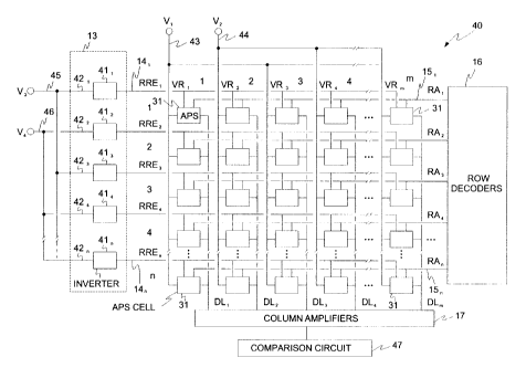
Figure 1 is a block diagram of a typical image sensor array;
Figure 2 is a circuit diagram of an active pixel sensor (APS) circuit;
CA 02340572 2001-03-13
7
Figure 3 is a circuit diagram of an active pixel sensor (APS) circuit in
accordance
with one embodiment of this invention;
Figure 4 is a block diagram of an image sensor array in accordance with one
embodiment of this invention;
Figure 5 is a schematic diagram of a multi-level voltage source used with the
present invention; and
Figure 6 is illustrates reset voltages and reset voltage enable signals used
in the
preferred embodiment of the present invention.
Detailed Description of the Invention
Referring to figure 1, there is shown a block diagram of a typical image
sensor
array 10. The sensor array 10 consists of active pixel sensor (APS) circuits
11 arranged
in rows 1 to n and columns 1 to m. The columns 1 to m of APS circuits 11 are
provided
a voltage Vdd from a voltage supply 12 through lines VRI to VR~,. In addition,
each row
1 to n of APS circuits 11 receive reset enable signals RRE1 to RREõ which are
nonnally
pulses of equal amplitude but spaced in time from a row reset control 13 on
lines 14, to
14n to reset the sensor circuits 11. Access to each horizontal row 1 to n of
APS circuits
11 is provided by applying individual access signals RA, to RAn which are
normally
pulses of equal amplitude but spaced in time via row lines 15, to 15r, from a
row address
decoder 16. The columns 1 to m ofAPS circuits 11are connected via data lines
DLI to
DLm which are coupled to column sense amplifiers 17 to amplify the image
signal. Thus
the rows 1 to n of circuits 11 are sequentially reset by signals RREI to RREõ
to detect the
incident light on the circuits 11 whereas the sequential sensing of the level
of incident
light in the rows 1 to n of circuits 11 is initiated by access signals RAI to
RAõ and
received on data lines DL, to DLm
CA 02340572 2001-03-13
8
A typical three transistor APS circuit 11 is illustrated in figure 2. The
circuit 11
consists of a photodiode 21 coupled to the source of a reset transistor 22 and
the gate of
a transistor 23 which acts as a source follower amplifier. The drains of the
reset
transistor 22 and the amplifying transistor 23 are normally connected to a
supply voltage
Vdd through a reset voltage line VRm. The amplifying transistor 23 source is
coupled
to a data line DLm through an access transistor 24. When activated, the reset
transistor
22 places charge on one node 25 of the photodiode 21 from the supply voltage
Vdd.
This charge is drained through the photodiode 21 at a rate proportional to the
intensity
of incident light on the photodiode 21. A signal proportional to this
intensity can be
read from the circuit 11 on the dataline DLm by enabling the access transistor
24. The
timing for resetting the circuit 11 and then for accessing circuit 11 is
controlled by
signals RREn applied to reset transistors 22 and by signal RAr, applied to
transistor 24.
The period of time between the two signals will be determined by the type of
readout
required for a specific application intended for the image sensor array 10.
During normal operation (i.e. image capture), the voltage Vdd supplied to the
drain of the reset transistor 22 is common to every circuit 11 (i.e. pixel) in
the array 10.
Each row 1 to n of circuits receives a reset enable signal RRE i to RREn
respectively via
a row reset line 141 to 14n. The reset enable signals RRE, to RREn are active
when at
a logical high and all have the same amplitude which may be substantially at
the level
of the supply voltage Vdd. Again, during normal operation, the voltage level
associated
with this logical high is common throughout the array. This means that all
photodiodes
21 in circuits 11 in the array 10 are reset to the same level, ie the same
amount of reset
charge is placed on the node of the photodiode 21 for every circuit 11.
The common reset voltage Vdd ensures that each circuit 11 will respond in a
similar manner if illuminated by light of a similar intensity. This is ideal
for image
capture operations but does not lend itself to the isolation of adjacent
circuits as would
be required if the array were to be tested electrically rather that optically.
CA 02340572 2001-03-13
9
In order to test the image sensor array 10 in accordance with the present
invention, different reset voltages are applied to the nodes 25 of the
photodiodes 21 in
at least adjacent sensor circuits 11 in the array 10. A predetermined period
of time after
the reset voltage has been applied, the voltage at each node 25 is sensed to
determine its
level. The detected level for each sensor circuit 11 which has been provided
with its
individual signature, may then be compared to an expected signal level for
that circuit
to determine if the circuit is faulty. In addition, if the detected levels for
adjacent sensor
circuits 11 are identical or very similar , it will be an indication that they
are shorted
together.
With reference to figure 1, one way of implementing the present invention is
to
provide different reset voltages to adj acent columns of sensor circuits 11
using lines VR I
to VRm. Thus, referring to figure 2, rather then have a common voltage Vdd,
the voltage
to the drain of transistor 22 in adjacent columns 1 to m would differ. In
addition, the
reset enable signal RRE, to RREr, would be generated at different active
voltage levels
for adjacent rows 1 to n of sensor circuits 11. Thus, referring to figure 2,
the reset enable
signals RRE, to RREn applied to the gates 26 of transistors 22 in adjacent
rows 1 to n
would result in different voltages being applied to nodes 22 in the sensor
circuits in
adjacent rows 1 to n. This ensures that each sensor circuit 11 will be reset
to a different
voltage level than its neighbors, ie the column neighbors will be different
because of
different reset voltages on lines VRI to VRn, and the row neighbors will be
different
because of the reset enable signals RRE1 to RREn on reset lines 141 to 14n.
Therefore,
it may be determined if an individual sensor circuit 11 is faulty by comparing
the value
of the signal received from the sensor circuit 11 to an expected level. In
addition, if any
one or more of the column lines or row lines are open circuited, groups of
sensor circuits
will appear to be inoperative, analysis will determine the faulty line. On the
other hand,
if column lines VRI to VR~, or data line DL, to DLn, are shorted to ground or
to one
another, similar readings will be seen from a series of sensor circuits 11 in
one or in
adjacent rows. Finally, if row lines 14, to 14,, or lines 151 to 15n are
shorted to ground
or to one another, similar readings will be seen from adjacent sensor circuits
11 in
adjacent rows. In this manner the entire sensor array may be tested for faults
by cycling
through the array 10 once.
CA 02340572 2001-03-13
It is noted that if different voltages are applied to the reset voltage lines
VR, to
VRm or to at least adjacent lines, similar transistors 23 in circuits 11 in
adjacent columns
I to m will also have different voltages applied to their drains causing the
transistors 23
to operate at different levels. This may be avoided by laying out sensor
circuits 11 of
5 the type illustrated in figure 3. The circuit 31 is similar to the circuit
11 illustrated in
figure 2 except that the drain of transistor 23 is connected to a supply
voltage Vdd line
32 which is common to all of the circuits 31 in the sensor array 10.
As will be described with regard to figure 4, there are a number of ways to
10 implement the present invention. Figure 4 illustrates a sensor array 40
that is similar to
the array 10 in figure 1 wherein common elements are identified by common
reference
numbers. The sensor circuits 31 are identified as the type of circuit
illustrated in figure
3 where a separate supply voltage Vdd is applied to transistors 23 via lines
32 which is
integrated on the chip but is not shown on figure 4 for clarity. Figure 4
further
schematically illustrates the row reset control 13 which includes inverters
41, to 41 n
adapted to generate reset enable signals RRE1 to RREn on reset lines 14, to
14"
respectively. The inverters 41, to 41r, are connected to voltage supply lines
42, to 42,
which determines the amplitude of the output signals RRE1 to RRE,,. Normally,
all lines
42, to 42r, and VRI to VRm are laid out on the die and connected together to a
common
supply Vdd via a single bond pad.
However in the array 40 in accordance with the present invention each of the
lines 42, to 42r, and VRI to VRm may be separate so that they may be connected
to
different voltage supplies to carry-out the testing of the array. This would
require either
a separate power supply pin for each voltage level, or number voltage
generators or
dividers integrated on the sensor array 40 chip. Such an implementation would
result
in a severe die area penalty.
In the preferred embodiment shown in figure 4, two voltage levels V, and V,
are
applied to the column reset voltage lines VR, to VR,õ via lines 43 and 44 and
two levels
of voltage V3 and V4 are applied to the rows 42, to 42r, via lines 45 and 46.
These
CA 02340572 2001-03-13
11
voltage signals are illustrated in figure 6. The embodiment may be further
simplified
by applying the same two voltage levels VI and V2 to the column voltage reset
lines
VRI to VR,, by connecting lines 43 and 44 respectively as well as to the rows
42, to 42,
by connecting lines 45 and 46 respectively. Thus one level V, would be
provided to
the odd numbered rows 421, 423,.... and columns VRI, VR3, .... while the
second level
V2 would be provided to the even numbered rows 422, 424, ....and columns VR,,
VR4,
..... Within the scope of the present invention, other combinations of voltage
levels are
also possible.
The two voltage levels VI and V2 of the preferred embodiment can be provided
by an external source through two bond pads where one pad is already connected
to a
regular supply voltage Vdd. Once tested, if it is concluded that the die is
not defective,
the pads can be shorted together for normal operation. When the die is
configured as
such, the array will then receive only a single supply voltage Vdd.
In another embodiment of the invention as illustrated schematically in figure
5,
a voltage level generator 50 may be integrated on the die which would include
a single
bond pad 51 for an external power supply Vdd. Circuits for boosting voltage
levels such
as charge pumps and circuits for stepping down voltage levels are well known
in the art.
The generator could provide any number of output voltages required for the
testing of
the sensor array 40.
As described above, defects are identified by comparing the signals received
on
data lines DL, to DL,, to expected values. This comparison can be accomplished
off
chip by a test system; however, a comparison circuit 47 may be integrated on
the chip
to determine if the signals received on data lines DLl to DLR,. agree with the
expected
data. This would greatly reduce the amount of complexity required of the
system used
to test the die. When combined with on chip voltage generators, this circuitry
could be
used as part of a built in self test (BIST) function.
CA 02340572 2001-03-13
12
The main advantage of the present invention is the ease through which
independent APS circuits 11, 31 are tested. A further advantage of the present
invention
is the minimization of peripheral circuitry necessary to distribute the
differing voltages
to adjacent rows and columns in the array. Yet another advantage of the
current
invention is the ability to test all of the row lines and data lines on an
individual basis,
resulting in faster interpretation of faults which reduces the time required
to correct
problems. These advantages are achieved together with the reduction of
manufacturing
testing dependency on an external calibrated light source in order to reduce
the cost of
such a light source or totally eliminate its requirement for a certain class
or grade of
imaging products.
Several design variations are possible with the described architecture. Though
the present invention was described with regard to one structure of an APS
circuit 11,
31 referred to as a three transistor (3T) structure, it is possible to vary
this basic circuit
structure and still perform the tests in accordance with the invention. Other
possible
APS circuits include but are not limited to 4T and 5T structures of which
there are
several variations.
The built in self test (BIST) embodiment in accordance with this invention
lends
itself to the possibility of using it for applications other than testing
during
manufacturing. One application could be for an image sensor used in a system
which
is controlled remotely, potentially in a satellite or some other location
requiring such
control. If the system were to malfunction, the BIST capability would allow
the
operator to test the sensor to determine if the fault was with components of
the image
sensor or some other component in the system.
While the invention has been described according to what is presently
considered
to be the most practical and preferred embodiments, it must be understood that
the
invention is not limited to the disclosed embodiments. Those ordinarily
skilled in the art
will understand that various modifications and equivalent structures and
functions may
be made without departing from the spirit and scope of the invention as
defined in the
CA 02340572 2001-03-13
13
claims. Therefore, the invention as defined in the claims must be accorded the
broadest
possible interpretation so as to encompass all such modifications and
equivalent
structures and functions.