Note: Descriptions are shown in the official language in which they were submitted.
CA 02340653 2001-02-15
LAYERED DIELECTRIC ON SILICON CARBIDE SEMICONDUCTOR STRUCTURES
FIELD OF THE INVENTION
The present invention relates to high power, high field, or high temperature
silicon carbide devices and in particular relates to insulated gate field
effect
transistors, device passivation, and field insulation.
BACKGROUND OF THE INVENTION
The present invention relates to silicon carbide devices particularly
insulated
gate devices and devices that incorporate device passivation, edge
termination, or
l0 field insulation, and that are formed in silicon carbide because of silicon
carbide's
advantageous physical and electronic characteristics.
For electronic devices, particularly power devices, silicon carbide offers a
number of physical, chemical and electronic advantages. Physically, the
material is
very hard and has an extremely high melting point, giving it robust physical.
15 characteristics. Chemically, silicon carbide is highly resistant to
chemical attack and
thus offers chemical stability as well as thermal stability. Perhaps most
importantly,
however, silicon carbide has excellent electronic properties, including high
breakdown field, a relatively wide band gap (about 2.9 eV at room temperature
for the
6H polytype), high saturated electron drift velocity, giving it significant
advantages
20 with respect to high power operation, high temperature operation, radiation
hardness,
and absorption and emission of high energy photons in the blue, violet, and
ultraviolet
regions of the spectrum.
Accordingly, interest in silicon carbide devices has increased rapidly~and
power devices are one particular area of interest. As used herein, a "power"
device is
25 one that is designed and intended for power switching and control or for
handling
high voltages and large currents, or both. Although terms such as "high field"
and
"high temperature" are relative in nature and often used in somewhat arbitrary
fashion, "high field" devices are generally intended to operate in fields of 1
or more
megavolts per centimeter, and "high temperature" devices generally refer to
those
30 operable above the operating temperatures of silicon devices; i.e., at
least 200°C and
preferably 250°-400°C, or even higher. For power devices, the
main concerns include
the absolute values of power that the device can (or must) handle, and the
limitations
CA 02340653 2001-02-15
18-OQ~2000 US 009919775
2
on the device's operation that are imposed by the characteristics and
reliability of the
materials used.
Silicon carbide-based insulated gate devices, particularly oxide-gated devices
such as MOSFETs, must, of course, include an insulating material in order to
operate
as IGFETs. Similarly, MI5 capacitors require insulators. By incorporating the
insulating material, however, some of the physical and operating
characteristics of the
device become limited by the characteristics of the insulator rather than by
those of
silicon carbide. In particular, in silicon carbide MOSFETs and related
devices, silicon
dioxide (Si02) provides an excellent insulator with a wide band gap and a
favorable
Io interface between the oxide and the silicon carbide semiconductor material.
Thus,
silicon dioxide is favored as the insulating material in a silicon carbide
IGFET.
Nevertheless, at high temperatures or high fields or both, at which the
silicon carbide
could otherwise operate satisfactorily, the silicon dioxide tends to
electrically break
down; i.e., to develop defects, including traps that can create a current path
from the
15 gate metal to the silicon carbide. Stated differently, silicon dioxide
becomes
unreliable under the application of high electric fields or high temperatures
(250°-
400°C) that are applied for relatively long time periods; i.e_, years
and years. It will
be understood, of course, that a reliable semiconductor device should have a
statistical
probability of operating successfully for tens of thousands of hours. Devices
2o incorporating silicon dioxide are discussed in Agarwal, et aL, A Critical
Look at the
Performance Advantages and Limitations of 4H SiC Power UMOSFET Sty-uctures,
Proceedings of the International Symposium on Power Semiconductor Devices and
IC's, New York, IEEE, vol. Symp. 8, 1996, pages 119-122, XP000598411; Agarwal
et al., Temperature Dependence of Fowler-NoYdheim Cu~~ent in 6H arid 4H SiC
MOS
25 Capacitors, IEEE Electron Device Letters, Vol. 18, No. 12, 1/12/97, pp. 592-
594,
XP000727109; EP-A-0637069; and WO 97/39485.
Additionally, those familiar with the characteristics of semiconductors and
the
operation of semiconductor devices will recognize that passivation also
represents a
challenge for structures other than insulated gates. For example, junctions in
devices
3o such as mesa and planar diodes (or the Schottky contact in a metal-
semiconductor
FET) produce high fields that are typically passivated by an oxide layer, even
if
REPLACEMENT SHEET AM E N D E D S H E ET
CA 02340653 2001-02-15
i 8-09-2000 US 009919775
2/1
otherwise non-gated. Such an oxide layer can suffer all of the disadvantages
noted
above under high field or high temperature operation.
Accordingly, IGFET devices formed in silicon carbide using silicon dioxide as
the insulator tend to fall short of the theoretical capacity of the silicon
carbide because
of the leakage and the potential electrical breakdown of the silicon dioxide
portions of
the device.
Although other candidate materials axe available for the insulator portion of
silicon carbide IGFETs, they tend to have their own disadvantages. For
example,
REPLACEMENT SHEET AMENDED SHEET
CA 02340653 2001-02-15
3
high dielectrics such as barium strontium titanate or titanium dioxide have
dielectric
constants that drop dramatically when a field is applied. Other materials have
poor
quality crystal interfaces with silicon carbide and thus create as many
problems (e.g.,
traps and leakage current) as might solved by their high dielectric constant.
Others
such as tantalum pentoxide (TaZ05) and titanium dioxide (Ti02) tend to exhibit
an
undesired amount of leakage current at higher temperatures. Thus, simply
substituting other dielectrics for silicon dioxide presents an entirely new
range of
problems and disadvantages in their own right.
Recent attempts to address the problem have included the techniques
to described in U.S. Patent No. 5,763,905 to Harris, "Semiconductor Device
Having a
Passivation Layer." Harns '905 appears to be somewhat predictive, however, and
fails to report any device results based on the disclosed structures.
Therefore, the need exists for a dielectric composition or structure that can
reliably withstand high electric fields while minimizing or eliminating
current
leakage, and while operating at high temperatures in order to take full
advantage of
silicon carbide's electrical characteristics.
OBJECT AND SUMMARY OF THE INVENTION
Therefore, it is an object of the present invention to provide dielectric
structures for silicon carbide-based IGFETs that can take advantage of the
power
handling capabilities of silicon carbide.
The invention meets this object with a dielectric structure for silicon
carbide
devices that comprises a layer (or device) of silicon carbide, a layer of
silicon. dioxide
on the silicon carbide layer, a layer of another insulating material on the
silicon
dioxide layer, with the insulating material having a dielectric constant
higher than the
dielectric constant of silicon dioxide, and a gate contact (for gated devices)
to the
insulating material. In preferred embodiments the dielectric structure
includes a
capping layer of Si02 beriveen the high dielectric and the gate.
In another aspect, the invention provides insulated gate devices such as
MISFETs that incorporate the inventive dielectric structure as the gate
insulator.
3o In another aspect, the invention provides passivation, edge termination, or
field insulation for silicon carbide devices.
CA 02340653 2001-02-15
4
In another aspect, the invention provides a high power semiconductor device
for which the active portions are formed of silicon carbide, and that include
passivation portions that experience high fields under an applied potential.
These
passivation portions are in turn formed of a layer of silicon dioxide on a
portion of the
silicon carbide, a layer of another insulating material on the silicon dioxide
that has a
dielectric constant higher than the dielectric constant of silicon dioxide,
and a capping
layer of silicon dioxide on the high dielectric layer.
The foregoing and other objects and advantages of the invention and the
manner in which the same are accomplished will become clearer based on the
1o following detailed description taken in conjunction with the accompanying
drawings
in which:
~RIEF DESCRIPTION OF THE DRAWINGS
Figure 1 is a cross-sectional view of a first embodiment of the present
invention;
Figure 2 is a similar view of a second embodiment of the invention;
Figure 3 is a cross-sectional view of an IGFET according to the present
invention;
Figure 4 is a cross-sectional view of an MIS capacitor according to the
present
invention;
2o Figure 5 is a comparison plot of electron mobility versus gate voltage for
conventional thermal oxides and insulators according to the present invention;
Figure 6 is a cross-sectional view of a planar diode passivated according to
the
present invention;
Figure 7 is a comparative plot of device lifetimes versus electric field;
Figure 8 is a cross-sectional view of another field-effect device according to
the present invention; and
Figure 9 is another comparative plot of device lifetimes versus electric
field.
DETAILED DESCRIPTION
The present invention is a dielectric structure for wide bandgap semiconductor
3o materials and related devices formed from such materials. A device
structure
according to the present invention, in particular a basic MIS capacitor, is
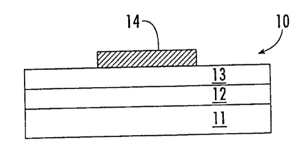
illustrated in
Figure 1 and is broadly designated at 10. The structure comprises a layer of
silicon
CA 02340653 2001-02-15
carbide 11 which can be a substrate portion or an epitaxial layer of silicon
carbide.
The manufacture of such single crystal silicon carbide substrates and the
various
epitaxial layers can be earned out according to various techniques described
in U.S.
patents that arc commonly assigned (or licensed) with the present invention.
These
5 include but are not necessarily limited to Nos. Re. 34,861; 4,912,063;
4,912,064;
4,946,547; 4,981,551; and 5,087,576, the contents of all of which are
incorporated
entirely herein by reference. The substrate or epitaxial layer can be selected
from
among the 3C, 4H, 6H, and 15R polytypes of silicon carbide with the 4H
polytype
being generally preferred for high power devices. In particular, the higher
electron
mobility of the 4H polytype makes it attractive for vertical-geometry devices.
The
device structure 10 next includes a layer of silicon dioxide 12 on the silicon
carbide
layer. Silicon dioxide has an extremely wide bandgap (about 9 eV at room
temperature) and forms an excellent physical and electronic interface with
silicon
carbide. Thus, it is a preferred insulator for many purposes with the
exception that, as
noted in the Field and Background, it can exhibit characteristic weaknesses at
high
temperatures under high fields.
Accordingly, the invention further includes a layer 13 of another insulating
material on the silicon dioxide layer 12. The layer 13 is selected as having a
dielectric
constant (~) higher than the dielectric constant of silicon dioxide, and also
has
physical and chemical characteristics that enable it to withstand the high
temperature
operation for which the silicon carbide portion of the device is intended. In
preferred
embodiments, the high dielectric material is selected from (but not limited
to) the
group consisting of silicon nitride, barium strontium titanate ((Ba,Sr)Ti03),
titanium
dioxide (Ti02), tantalum pentoxide (Ta205), aluminum nitride (AlN), and
oxidized
aluminum nitride, with silicon nitride and oxidized aluminum nitride being
particularly preferred, and with silicon nitride (Si3N4) being most preferred.
The gate
contact 14 is made to the insulating material layer 13 for permitting a bias
to be
applied to the device structure.
Figure 2 illustrates a second embodiment of the device (also a MIS capacitor)
3o broadly designated at 15. As in Figure 1, the second embodiment includes a
silicon
carbide layer 16 (epitaxial or substrate), the first silicon dioxide layer 17,
the
insulating material 20 selected according to the criteria noted above, and a
second
CA 02340653 2001-02-15
18-~9-200 US 009919775
6
layer of silicon dioxide 21 between the gate contact 22 and the insulating
layer 20.
The second silicon dioxide layer 21 provides a barner to prevent charge from
passing
between the gate metal and the high dielectric material.
In preferred embodiments, the silicon dioxide layers 12 or 17 are thermally
formed following which the insulating layers 13 or 20 are deposited by
chemical
vapor deposition (CVD). The insulating layers can, however, be formed by any
appropriate technique, e.g., certain oxides can be formed by sputter-
depositing a metal
and then oxidizing it. As another example, Si3N4 can. be deposited by plasma-
enhanced CVD (PECVD). Because the Si02 layer 12 or 17 serves to prevent
to tunneling, it does not need to be exceptionally thick. Instead, the Si02
layer is
preferably maintained rather thin so that the extent of thermal oxidation can
be
limited. As recognized by those familiar with these materials, implantation
can affect
the manner in which SiC oxidizes. Thus, if extensive oxidation is carried out
on a
device or precursor having implanted SiC portions, the resulting oxidized
portions
will differ in thickness from one another, a characteristic that can be
disadvantageous
in certain circumstances. Accordingly, limiting the extent of oxidation helps
minimize or eliminate such problems. Alternatively, the oxide can be deposited
(e.g.,
by CVD) to avoid the problem altogether.
In preferred embodiments, the first silicon dioxide layer 17 or 12 is no more
than about 100 angstroms thick while the layer of insulating material (13 or
20) can
be about 500 angstroms thick. Stated differently, each of the oxide layers
represents
between about 0.5 and 33 percent of the total thickness of the passivation
structure,
with the insulating material making up the remainder. In preferred
embodiments, the
oxide layers are each about 20 percent of the total thickness and the
preferred nitride
insulator is about 60 percent of the total thickness.
Figures 3 and 4 illustrate a respective IGFET and MIS capacitor according to
the present invention. Figure 3 shows an IGFET broadly designated at 24 with a
first
silicon carbide portion 25 having a first conductivity type. A gate insulator
structure
according to the present invention is on the first silicon carbide portion 25
and is
designated by the brackets 26. Taken individually, the gate insulator includes
the
Layer of silicon Dioxide 27 and the layer of an insulating material 30 that
has the
dielectric constant higher than the dielectric constant of silicon dioxide. In
the
REPLACEMENT SHEET A M E N D E D S H E ET
CA 02340653 2001-02-15
embodiment illustrated is Figure 3, the insulator 26 further includes the
second layer
31 of silicon dioxide. The IGFET of Figure 3 further includes a gate contact
32 and
respective second and third portions of silicon carbide 33 and 34 that have
the
opposite conductivity type from the first silicon carbide portion 25.
Respective ohmic
contacts 35 and 36 are made to the portions 33 and 34 to form the source and
drain
portions of the FET. As indicated by the dotted lines in Figure 3, devices
such as the
IGFET 24 can be segregated from one another using a field oxide 37. Those
familiar
with such devices and with integrated circuits made from them will recognize
that the
field oxide portions 37 serve to segregate the device from other devices.
Although the
to field oxide is not directly electronically related to the gate insulator
portion 26, the
insulator structure of the present invention can provide similar advantages as
a field
insulator.
Figure 4 illustrates an MIS capacitor according to the present invention and
in
particular a variable capacitance device analogous to that set forth in U.S.
Patent No.
15 4,875,083, the contents of which are incorporated herein by reference. The
capacitor
in Figure 4 is broadly designated at 40 and comprises a doped silicon carbide
portion
41 and a capacitance insulator portion on the dope silicon carbide portion.
The
capacitance insulator portion includes a layer of silicon dioxide 42 on the
silicon
carbide portion, a layer 43 of the other insulating material with the
dielectric constant
2o higher than the dielectric constant of silicon dioxide. In the embodiment
illustrated in
Figure 4, the capacitor 40 also includes the second layer 44 of silicon
dioxide between
the other insulating material layer 43 and the gate contact that is
illustrated at-45. The
contact 45 can be made of metal or an appropriate conductive semiconductor
such as
polysilicon that is sufficiently doped to give the required contact
characteristics. An
25 ohmic contact 46 which in the illustrated embodiment forms a ring, two
sections of
which are shown in the cross-sectional view of Figure 4, is made to the doped
silicon
carbide portion 41 so that a bias applied to the metal contact 45 variably
depletes the
doped silicon carbide portion 41 to correspondingly vary the capacitance of
the
capacitor 40. As in the embodiment in Figure 3, field oxide portions 47 can
also be
3o typically included to segregate the device from its neighbors. As noted
above, the
portions 47 can also incorporate the dielectric structure of the present
invention.
CA 02340653 2001-02-15
Those familiar with semiconductor devices will understand that the
illustrations of Figures 1-4 and 6 are exemplary, rather than limiting, in
their
representations of various insulated gate and metal-insulator-semiconductor
structures. Thus, although Figures 1-4 and 6 show generally planar structures
and
devices, it will be understood that the insulator structures of the present
invention can
be applied to a wider variety of device geometries, for example UMISFETs.
Other
gated structures for which the dielectric structure of the invention is useful
include
MISFETs, insulated gate bipolar transistors (IGBTs), MOS-turn off thyristors
(MTOs), MOS-controlled thyristors (MCTs) and accumulation FETs (ACCUFETs).
Non-gated structures for which the invention can provide enhanced passivation,
edge
termination, or field insulation include p-i-n diodes, Schottky rectifiers,
and metal-
semiconductor field-effect transistors (MESFETs).
The invention also provides the same advantages for particular structures
including lateral power MOSFETs and double diffused MOSFETs (DMOSFETs),
IS which are vertically oriented devices (i.e., with source and drain on
opposite surfaces
of the substrate). Exemplary devices are described in U.S. Patents 5,506,421
and
5,726,463; the contents of both of which are incorporated entirely herein by
reference.
Additional exemplary devices are set forth in co-pending U.S. applications
Serial Nos.
08/631,926 filed April 15, 1996 ("Silicon Carbide CMOS and Method of
2o Fabrication"); b9/093,207 filed June 8, 1998 ("Self Aligned Methods of
Fabricating
Silicon Carbide Power Devices by Implantation and Lateral Diffusion"); and
09/093,208 filed June 8, 1998 ("Methods of Forming Silicon Carbide Power
Devices
by Controlled Annealing"); and the contents of these applications are likewise
incorporated entirely herein by reference.
25 , Figure 8 illustrates a double-diffused or double-implanted MOSFET broadly
designated at 60 that incorporates the insulator structure of the present
invention. As
illustrated in Figure 8, the transistor source is formed by n+ regions 61
within p-type
wells 62 which are incorporated into a silicon carbide portion shown as the
epitaxial
layer 63 in the manner described in the above-referenced applications. The
region 63
30 represents the drain drift region of the transistor with the n+ drain being
illustrated at
64, a drain contact at 65, and an appropriate wire lead at 66. Similarly, the
source
contacts are respectively shown at 67 with their wire leads 70. The gate
insulator
CA 02340653 2001-02-15
9
structure is formed according to the present invention and in preferred
embodiments
includes the first silicon dioxide layer 71, a silicon nitride layer 72, and a
second
silicon dioxide layer 73. A gate metal contact 74 and its wire lead 75
complete the
structure. In operation, the p-type regions 62 are depleted to form an
inversion layer
when a bias is applied to the gate contact 74. Those familiar with these
devices will
also recognize that if the drain portion 64 were to be changed in this
structure from n+
conductivity to p-type conductivity, the resulting illustration would
represent an
insulated gate bipolar transistor (IGBT).
The illustrated structures improve the gate or field passivation by layering
the
l0' second dielectric material over the silicon dioxide. The silicon dioxide
continues to
provide a large electrical barrier (i.e., its 9 eV bandgap) on silicon carbide
and
prevents the layered dielectric from leaking current. In complementary
fashion, the
additional dielectric material (with its higher dielectric constant) improves
the high
temperature and high field reliability as compared to a single dielectric
layer. Thus,
15 the layered dielectric combines the functional strengths of the two
different materials
to form a better dielectric on silicon carbide than could be attained with a
single
material. Additionally, silicon dioxide forms a better interface, in ternls of
electrically
charged or active states, with silicon carbide than does any other dielectric
material.
The dielectric constant of the material selected to be layered with the
silicon
2o dioxide is an important consideration because the field in the dielectric
will be
directly related to the field in the nearby silicon carbide and further
related to the ratio
of the dielectric constants of the layered dielectric and the silicon carbide.
Table 1
summarizes the dielectric constant for some common semiconductor devices and
also
lists silicon carbide as the figure of merit.
25 TABLE 1
DielectricCritical Operating sEo
Material Constant Field Field (MV/cm)
(MV/cm) (MV/cm)
SiC 10 3 3 30
Thermal SiOZ 3.9 11 2 7.8
Deposited 3.9 11 2 7.8
Si02
Si3N,~ 7.5 11 2 1 S
ONO 6 11 ~2 ~12
A1N 8.4 10-12 ~3$ ~30
AlO:N 12.4 8$ ~l$ ~12
SixNYOZ 4-7 11 ~2 ~8-14
(Ba,Sr)Ti03 75-250* 2$ --0.1''' ~8
TiOz 30-40 6 ~0.2$ -r4
CA 02340653 2001-02-15
1~
$ Estimated.
constant of (Ba,Sr)Ti03
In Table 1, the Critical Field represents the field strength at which the
material
will break down immediately. The Operating Field (Eo) is the highest field
that is
expected to cause little or no degradation to the dielectric for a
satisfactory time
period, e.g., at least 10 years.
The invention improves the reliability of the gate or field passivation on
silicon carbide by utilizing a dielectric material with a higher dielectric
constant than
silicon dioxide. In this regard, Gauss' Law requires the field in the
dielectric to be the
field in the semiconductor multiplied by a factor Of
(Ss~miconductor~~dielectric).
Accordingly, materials with dielectric constants higher than the dielectric
constant of
silicon carbide will have a lower electric field than the nearby silicon
carbide.
Accordingly, a critical measure of a material's applicability as a gate
dielectric or
passivating material for power devices is the product of field strength (E)
and
dielectric constant (s). Ideally the product of EE would exceed that of
silicon carbide.
In this regard, Table 1 lists several dielectrics that could be potentially
layered
with silicon dioxide to create an insulator structure that has better
electrical
characteristics than either of the two materials alone. Nevertheless,
additional
materials may be used in a dielectric structure and the selection is not
limited to those
in Table 1.
The layered dielectric of the invention has four important characteristics
that
enable silicon carbide MIS devices to operate at high temperatures or at high
gate
voltages: First, the bulk of the dielectric can be deposited, thus avoiding
thermal
consumption of SiC. As noted earlier, thermally grown silicon dioxide tends to
consume silicon carbide more rapidly over implanted regions thus resulting in
a
physical step and higher fields at the edge of an implanted region. Second,
the Si02
portion of the insulator structure has a high quality interface with silicon
carbide.
Third, the multilayer structure minimizes leakage currents at high
temperatures (250-
400°C). Fourth, the non-Si02 portion contributes a relatively high
dielectric constant
thus lowering the field in the non-Si02 dielectric as dictated by Gauss' Law.
CA 02340653 2001-02-15
lI
In producing a particular structure, the physical thickness of the layered
dielectric of the invention generally will be different than that of a single
dielectric
layer, with the difference being determined by the ratias of the dielectric
constants.
Additionally, to date, the layered dielectric is most preferably structured
with silicon
dioxide as the bottom layer (i.e., the one in contact with the silicon
carbide), because
this is required for acceptable leakage cun-ents at high temperatures.
~VIIS CAPACITORS
Capacitors were fabricated using the materials in Table 2 and including those
of the present invention. In a preferred embodiment, a three-step process was
used to
to produce respective silicon dioxide, silicon nitride, and silicon dioxide
layers. First,
high quality silicon dioxide was thermally grown on silicon carbide in an
oxidation
furnace to a thickness of about 100 angstroms (~). A preferred oxidation
technique is
set forth in co-pending and commonly assigned application Serial No.
08/554,319,
filed November 8, 1995, for "Process for Reducing Defects in Oxide Layers on
15 Silicon Carbide," the contents of which are incorporated entirely herein by
reference.
Next a 500 ~ nitride layer was deposited using low pressure chemical vapor
deposition (LPCVD) with silane (SiH4) and ammonia (NH3) as the source gases.
This
nitride layer was then oxidized in a wet ambient atmosphere at 950°C
for three hours
to form a second layer of silicon dioxide that was between about 50 and 100
2o angstroms thick.
DC leakage currents were measured on these MIS capacitors over a range of ~
1 S volts. Such a voltage corresponds to a field of approximately 3 megavolts-
per
centimeter. Table 2 summarizes the leakage currents in microamps per square
centimeter (~A/cm2) measured on different MIS capacitors. Capacitors that have
25 minimal leakage at room temperature were then measured at 250°C. The
leakage at
this temperature is identified in the Table as the "HT leak." A dash indicates
no
measurable leakage (less than 500 picoamps), while "too high" indicates
insulators
whose room temperature leakage was so high that no 250°C measurement
was
performed.
CA 02340653 2001-02-15
12
TABLE 2
6HP 6HN 4HN
Thermal SiOz Leak= - - -
HT Leak= - - -
LPCVD Si02 Leak= - - -
HT Leak= - - -
Silicon Nitride Leak= - - -
HT Leak= 56 1 1
ONO Leak= - - ~ -
HT Leak= - - -
A1N Leak= 125 250,000 >1000000
HT Leak= too high too high too high
AlO:N Leak= - - -
HT Leak= 2 >lE6 >lE6
As Table 2 demonstrates several dielectrics do not insulate well on silicon
carbide with some, such as aluminum nitride, lacking satisfactory
characteristics even
at room temperature. Only the structures that included silicon dioxide
insulated well
on silicon carbide at 250°C. This is most likely related to the bandgap
of the
dielectric material and the resulting low band offsets (barrier heights) with
silicon
carbide. Silicon carbide has a bandgap of about 3 eV and for a material to
insulate, a
barrier height of at least about 2 eV is desired. Thus, on silicon carbide,
the dielectric
l0 material or structure should have a bandgap of at least about 7 eV:
Standing alone,
silicon nitride, with a bandgap of 6 eV was thus expected to-and did-
demonstrate
problems, as shown by the leakage current measurements reported in Table 2.
The
bandgap of aluminum nitride (6.2 eV) is not very different than that of
silicon nitride,
and aluminum nitride has substantially higher leakage currents. The leakage
currents
demonstrated by the aluminum nitride and the silicon nitride prevent these
materials
from being useful as sole gate dielectrics. Additionally, further analysis of
these
insulators was limited to evaluating the net oxide charge.
Although a dielectric must have high reliability for high temperature high
field
device passivation applications, such reliability represents a necessary, but
not a
sufficient characteristic, to make it applicable for the gate layer of an MIS
device. For
such applications, charged bulk defects and electrically active interface
defects must
be minimized. Charged bulk defects will tend to cause voltage shifts in the
device,
while electrically active interface defects will degrade the channel mobility.
CA 02340653 2001-02-15
13
Charged bulk defects are traditionally referred to as "fixed oxide charge" and
are measured by the flatband voltage determined by a room temperature high
frequency capacitance-voltage (CV) curve. Any difference between the actual
voltage
at which flatband capacitance occurs and the ideal value, accounting for metal-
semiconductor work functions, is attributed to this fixed oxide charge. For
wide
bandgap semiconductors such as silicon carbide, however, the term "fixed"
oxide
charge is a misnomer. This calculated charge density includes vcontributions
from
interface states, many of which appear fixed at room temperature. For this
reason,
this calculated charge density is referred to herein as a "net" oxide charge.
1o Electrically active defects at the dielectric-semiconductor interface are
termed
interface states. These states can severely degrade the channel mobility of an
MIS
devices by either trapping and releasing the electrons, or by providing a
charged site
which would apply a force normal to the current flow. Either of these effects
will
inhibit current flow and subsequently reduce the channel mobility.
Accordingly, Table 3 compares the net oxide charge densities and minimum
measured interface state densities of the various capacitors.
TABLE 3
Net Oxide Charge (1011 cm 2)
Insulator 6H P-type 6H N-type 4H N-type
Thermal SiOz 6.9 -10.8 -26
LPCVD Si02 7.5 -11.5 -29
Silicon NitrideLeaky -9.7 -S 1
ONO 130 1.9 5.9
A1N 64 -26 -54
AlO:N 8.9 1.3 -5.2
Interface State Densities (101° cm-2eV'1)
Insulator 6H P-type 6H N-type 4H N-type
Thermal Si02 6.2 36 210
LPCVD SiOz 7.5 18 270
Silicon NitrideLeaky 240 1500
ONO 74 5.7 14
A1N 650 leaks leaks
AlO:N ~50 leaks leaks
The net oxide charge and interface state densities are the lowest on thermal
oxides and the LPCVD oxides, with no significant differences seen between
these
CA 02340653 2001-02-15
14
samples. For the n-type samples, the net oxide charge and interface state
densities are
significantly lower on the silicon dioxide/silicon nitride/silicon dioxide
sample (also
referred to herein as "ONO" structures). The silicon carbide/insulator
interface
quality is obviously superior when silicon dioxide forms the interface with
the silicon
carbide.
As shown in Table 4, the silicon dioxide layers had the highest breakdown
fields, especially at high temperature, regardless of the manner in which they
were
grown or deposited. The 1100°C thermally grown oxides had the highest
breakdown
fields, with the deposited oxides being almost as high.
l0 Although the breakdown field is important, the dielectric must also be
considered. Table 4 lists breakdown fields (EB) averaged across the three
wafer types
(where possible) and then multiplied by the empirical dielectric constant (E)
for both
room temperature and 350 °C measurements. The highest products of EBE
were
measured on the ONO, the thermally grown oxide, the deposited oxide, and the
aluminum oxy nitride.
TABLE 4
Maximum Breakdown Field (MV/cm)
Room Temperature
6H P 6H N 4H N E x (EBD)
8.0 7.0 8.7 31
12.8 10.6 9.9 43
11.8 9.9 10.0 41
7.4 5.2 5.8 46
9.0 8.0 8.4 51
1 0.5 1 7
8.6 4.0 4.8 38
350°C
6H P 6H N 4H N g x (EBD)
8.0 7.6 8.0 31
10.6 7.8 7.5 34
7.2 8.6 5.9 28
3.0 3.9 3.2 25
5.9 6.1 5.9 36
_ _ .. Leaks
-
5 - - ~ 33
CA 02340653 2001-02-15
Time-bias measurements at 350°C taken on 6H n-type SiC MIS
capacitors are
shown in Figure 7. Here the measured points are shown by the symbols, and the
exponential least squares fit is shown by the lines. The lifetimes exhibited
by these
devices are low, which is partially due to the small sample size. However,
these
5 values are not atypical for oxides on n-type SiC at 350°C.
The ONO capacitors had the highest lifetimes, showing more than an order of
magnitude improvement in lifetime over both the deposited and thermal oxides
at a
given applied electric field. Although the p-type interface quality of ONO
capacitors
is not as good as the thermal or deposited oxides, the n-type interface
quality is better
l0 than any of the other materials.
~vIISFETs
In addition to the capacitors, several planar metal-insulator semiconductor
field effect transistors (MISFETs) were fabricated with thermal oxides and
with the
layered ONO dielectrics. An additional comparison ofthe robustness of the
15 MOSFETs was made by comparing a breakdown voltages of the different
dielectric
materials. The field strength of the dielectrics were measured at both room
temperature and 350°C, and the results are set forth in Table 5.
TABLE 5
RT BD RT BD 350C BD 350C BD
Insulator Voltage (MV/cm) Voltage (MV/cm)
(V) (V)
Thermal Si02 35 7 25 5
LPCVD Si02 45 9 35 7
ONO 80$ 11.4$ 45$ 6.4$
~ The dielectric did not actually breakdown at this voltage, but leaked.
As noted earlier, thermal oxidation results in a physical step, as the
implanted
source and drain regions oxidize faster than the non-implanted channel region.
Thermal oxides grown on implanted areas also tend to be weaker than those
grown on
non-implanted material. These two effects are combined in a thermally oxidized
MOSFET, where the step enhances the field and the region of the weakest oxide.
Thus the breakdown field of the thermally oxidized MOSFET is significantly
reduced
from the breakdown fields demonstrated by the MOS capacitors.
The deposited oxide has a higher breakdown field than the thermally grown
oxide, but the highest breakdown voltage was achieved with the ONO dielectric
CA 02340653 2001-02-15
16
layers. The field was slightly low at 350°C, but the breakdown voltage
is probably a
better indicator of device reliability because a silicon nitride gate
insulator must be
thicker in order to have the same gate capacitance. Thus the ONO structure
demonstrated almost double the high temperature breakdown voltage of the
thermally
oxidized devices.
The channel mobility of the fat FETs (a "fat" FET has a gate width
approximately equal to its gate length) was determined from the linear regime
of the
MISFET: The drain voltage was set a 0.25 volts, and the gate voltages stepped
from 0
to 10 volts in one volt steps. The mobility was calculated from the
conductance
between the various gate voltages, which is independent of the threshold
voltage.
Figure S compares the channel mobility of the MISFETs fabricated with layered
ONO
dielectrics to those with thermal oxides. The ONO MISFETs have a slightly
higher
mobility. Figure 5 thus shows that the ONO layered dielectric structure is at
least as
good as a thermal oxide in these devices.
An estimate of the MISFET device reliability at high temperatures was measured
by applying a gate voltage of 15V (3 MV/cm) to a 4 x 100 ~m gate, grounding
the
source, drain and substrate, and monitoring the gate current until a
compliance current
of 1 nA was reached. This compliance current corresponds to a current density
of 0.25
mA/cm2. The gate voltage was increased above the probable use-voltage of 5 V
to
2o accelerate this test.
Table 6 compares the high temperature reliability of the MISFETs fabricated
with layered ONO dielectrics with those having thermal and deposited silicon
dioxide.
The ONO MOSFETs have a significantly better high temperature lifetime, e.g.,
more
than a factor of 100x better. Additionally, a packaged MISFET operated
successfully
for 240 hours.
TA L
Device lifetimes at 350°C with a 15 V (3 MV/cm) gate bias
Insulator Lifetime
Dry Thermal Oxide 0.08 hour
Deposited Oxide 0.75 hour
ONO > 75 hours
ONO (Packaged, Estimated 240 hours
335C)
CA 02340653 2001-02-15
17
The ONO sample was wafer tested at 350°C for 75 hours without
failing. At
that point, it was decided to package devices for testing, because the device
metals
would oxidize if exposed to air for several days at 350°C. The packaged
parts were
then tested at 350°C. The exact temperature of the packaged devices
could not be
easily controlled, however, and thus the estimated testing temperature was
probably
closer to 335°C than to 350°C. Nevertheless, the ONO sample
survived for 10 days
(240 hours) at 335°C.
Figure 9 also shows the MISFET lifetimes for. comparison with the capacitor
results. The MISFETs with the dry-wet thermal oxide have a dramatically
reduced
to lifetime when compared with the capacitors. This is most likely due to the
physical
steps created at the source and drain regions by the accelerated growth of the
implanted regions. The deposited oxide MISFET failed very close to its
projected
time, but slightly lower. The ONO MISFET fails almost exactly where one would
predict from the MIS capacitor data.
Diodes
In addition to the MIS capacitors, a 4-wafer lot of planar diodes was
fabricated. A cross section of an exemplary device 50 is shown in Figure 6.
The top
p-layer S 1 was implanted with variable doses. A second implant, the Junction
Termination Extension (JTE) 52, was performed adjacent to the first implant to
2o reduce field crowding. Although the JTE implant helps reduce the field
crowding at
the edge of the device, a high quality dielectric 53 on the surface of the
wafer is
required for passivation. The shape of the planar diode was circular. The
dielectric
53 is formed of the oxide/nitride/oxide according to the present invention.
Specifically, all three layers were deposited by PECVD.
The fabrication was repeated for comparison purposes with PECVD Si3N4 and
PECVD Si02 as single layer insulators.
The mask set used for this device consisted of diodes with radii varying from
100 to 500 Vim, while the width of the JTE implant varied between 50 and 150
p.m.
The epitaxial layers should support 5 kV, but the JTE of these devices were
designed
3o to block only 3 kV in order to place more stress on the passivation. The
device
performance is more sensitive to the passivation, because the JTE implants do
not
terminate all of the fields generated by the higher voltage. Accordingly, the
CA 02340653 2001-02-15
is
passivation must withstand much larger fields. Thus, the devices were
deliberately
designed to help evaluate the various dielectric materials.
Five wafers were procured for the fabrication of high voltage P-i-N diodes.
4H n-type substrates for these devices had a 50 ~m epitaxial ri layer doped
about
1x10'5 crri 3 grown, and a 1.2 p.m p' layer doped 1x108 cm 3.
Figure 6 also illustrates the n-type portion of the device at 54, the anode at
55,
and the cathode at 56.
The fabrication of the diode began with etching alignment marks into the SiC
wafer for alignment of the future masks. The anode junction was defined by
etching
to through the top p-type layer in most of the surface, while leaving circular
p-type
anode regions exposed. Using a thick (1.4 pm) oxide mask, the regions
receiving the
low-dose JTE implant were defined. The thickness of the oxide mask and the
implantation energy and dosage of the p-type dopant (aluminum) were chosen so
that
only the intended termination region receives the implant while it is blocked
entirely
from regions where it is not intended. The junction region also received this
implantation step so that a high surface doping of the p-type layer was formed
for
ohmic anode contacts. The implanted aluminum was annealed to minimize the
damage from ion implantation and to electrically activate the implants.
The breakdown voltage was measured on each type of diode. The silicon
nitride had a great deal of leakage, and broke down at 2.6 kV. The oxide
devices had
low/no leakage and broke down around 3.5 kV. The devices incorporating the
dielectric structure of the invention had no leakage out to 5 kV, and broke at
a world-
record level of 5.9 kV.
In summary, the ONO dielectric of the present invention provides a significant
improvement. The high temperature lifetime of the OI~,~O layered MISFET is
more
than a factor of 100x better than the state-of the-art deposited oxide. This
has
immediate relevance to high temperature SiC power devices and circuits. By
projecting back to the likely rated operating field of 1 MV/cm, it can be
predicted that
ONO MOSFETs will have a lifetime of more than 240,000 hours at
335°C.
Thus, the success demonstrated to date on these several devices indicates that
the passivation of the present invention will be expected to work well on
almost all
passivation or insulated gate structures.
CA 02340653 2001-02-15
19
In the drawings and specification, there have been disclosed typical
embodiments of the invention, and, although specific terms have been employed,
they
have been used in a generic and descriptive sense only and not for purposes of
limitation, the scope of the invention being set forth in the following
claims.