Note: Descriptions are shown in the official language in which they were submitted.
CA 02340987 2001-02-16
WO 00/11628 1 PCT/SE99/01395
A METALLIC BUILDING ELEMENT FOR OPTOELECTRONICS
FIELD OF INVENTION
The present invention relates to a method of patterning
metallic building Elements and to a patterned metallic
building element, said building element being produced in
accordance with the method of patterning metallic building
elements, wherein the measurement accuracy obtained can lie
in the sub-micrometer range. The building elements produced
in accordance with the method may be used, among other
things, as carrier: for optoelectrical and electrical
components, and fibres and waveguides. The metallic building
elements may also be used as micromechanical building blocks
or as parts of a rnould cavity for injection moulding or
compression moulding purposes.
BACKGROUND ART
c0 The technique at present used for mounting optoelectric laser
chips in 1_ow-cost applications most often includes soldering
of a chip to a ceramic or silicon carrier. Alignment between
the optical active part of a laser and the core of a fibre
can be achieved by virtue of the possibilities of etching
c5 silicon with great precision and the use of a technique in
which the laser is firmly soldered and aligned with the aid
of the surface tension forces present in a solder melt. Some
sort of gluing techr,i.que is normally used, for instance, to
fasten pin diodes to a carrier. Optical mirrors produced by
..0 etching in silicon and metallising the surface are often used
to reflect light frorn a fibre to a pin diode.
When an optoelectric laser chip is to be mounted on a ceramic
carrier or a silicon carrier, there often arises the problem
35 of dissipating heat generating in the chip. Varying chip
temperature can, in operation, influence the transmitted
CA 02340987 2001-02-16
WO 00/11628 ~ PCT/SE99/01395
wavelength. An excessively high operating temperature can
also shorten the useful life of the chip. Furthermore,
ceramic and silicon carriers often demand a high price, due
to the relatively complicated manufacturing processes
involved.
SUMMARY OF THE INVENTION
The technique described in accordance with the invention
:LO enables the cost-effective production of building elements
that can be used either free-standing or as a substantial,
pattern-creating part in a mould cavity intended for
injection moulding or compression moulding purpoaes. The
technique can be used to create metallic carriers that have
:L5 low thermal resistance and good electrical conductivity, with
the intention of preventing damage to electrical and
optoelectrical chips, such as lasers, due to high oz- varying
temperatures.
:?0 With a starting point from a silicon original or master,
which can be etched to sub-micrometer precision and then
plated with a metal, such as nickel, on the silicon surface,
it is possible to produce a nickel shim with a precision and
a surface fineness that wiil still lie in the sub-micrometer
~5 range. If necessary, the rear side of the shim can then be
made flat prior to separating silicon from nickel. Subsequent
to removing the silicon master., a photo-sensitive material,
in liquid form or in film-form, can be used to create
cavities that reach down to the nickel shim. These cavities
30 can then be metallised, to form three-dimensional building
elements of high precision.
These metal precision elements can then be used, for
instance, for effectively conducting away heat from lasers or
35 other heat-generating chips. The precision, surface fineness
and measurement accuracy that can be achieved with the method
CA 02340987 2001-02-16
WO 00/11628 3 PCT/SE99/01395
also enable optoelectrical components, such as, e.g., lasers
with optical single-:mode fibres and sharp optical mirrors to
be aligned. The method also provides building elements that
can conduct electric ~~urrent, which enables three-dimensional
electric conductors and electrodes to be produced to a
specified thickness. The template or form produced in
accordance with the aforedescribed method can also be used
repeatedly in plating cycles, therewith contributing to low-
cost production of the plated building elements.
The invention will. now be described in more detail with
reference to a preferred embodiment thereof and also with
reference to the accompanying drawings.
1.5 BRIEF DESCRIPTION OF THE DRAWINGS
Figure la is a cross-sectional view of a micro-worked silicon
plate.
2.0 Figure lb is a cross-sectional view of the patterned silicon
plate covered with a thin metal film.
Figure lc is a cross-sectional view of the coated silicon
plate coated with a further metal layer.
;?5 Figure ld is a croas-sectional view of the coated silicon
plate where the metal layer coating in Figure lc has been
levelled or smoothed-off.
Figure le is a cross-sectional view of metallic layers that
30 remain subsequent to the removal of the silicon plate.
Figure if is a cross-sectional view of the remaining metal
layers covered with a separation layer.
CA 02340987 2001-02-16
WO 00111628 4 PCT/SE99/01395
Figure lg is a cross--sectional view of the remaining metallic
layers with the separation layer laminated with a photo-
sensitive material.
Figure lh is a cross-sectional view of the metallic layers
according to Figure lg exposed to light with the aid of a
photomask.
Figure li is a cross-sectional view of the metallic layers
according to Figure lh with dissolved parts.
Figure 1j is a cross-sectional view of the metallic layers
according to Figure :L.i with metal-filled cavities.
7.5 Figure 1k is a cross-sectional view of the metallic layers
according to Figure :1j with remaining photosensitive material
etched away.
Figure 11 is a croas-sectional view of various separated,
a?0 released and therewith formed building elements.
Figure lm is a cross-sectional view of remaining metallic
layers that can be reused as moulds or templates according to
Figure lg.
;? 5
DESCRIPTION OF PREFERRED EMBODIMENTS
Figure la illustrates a micro-worked silicon plate 1. The
resultant pattern c:an be obtained in one or more of the
30 following ways: dry etching, wet etching, laser processing or
spark processing.
Figure lb shows how a thin metal layer 2, a so-called start
layer, has been sputtered or vaporised on the patterned
35 silicon plate 1 to enable subsequent initiation of a plating
process.
CA 02340987 2001-02-16
WO 00/11628 PCT/SE99101395
Figure lc shows how a metal 3, and then preferably nickel,
has been plated on the thin metal layer 2 on the silicon
plate l, t=o provide a so-called nickel shim on the start
layer.
Figure ld shows how the nickel shim 3 firmly seated on the
silicon plate 1 has been levelled or smoothed by some
mechanical process, for instance by smooth grinding or
1~ polishing.
Figure le shows how the silicon plate 1 and the nickel shim 3
have been separated from one another after being reversed.
Figure if shows how t:he nickel shim 3 has beer. coated with a
separation layer 4 on the existing start layer 2, said
separation layer enabling separation in a later stage, as
described hereinafter with reference to Figure 11, but does
not prevent plating, see hereinafter with reference to Figure
lj.
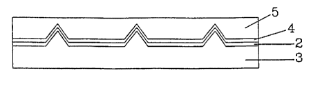
Figure lg shows how the nickel shim 3 with layers 2 and 4 has
been laminated with a. photo-sensitive material 5.
Figure lh shows how selective parts of the photo-sensitive
material 5 have been exposed to light, with the aid of a so-
called photomask 6. '
Figure li shows how the photo-sensitive material has been
~~0 developed, wherewith those parts that have been exposed to
light have been dissolved in a developer to form cavities 9,
leaving parts of non--exposed photo-sensitive material 7. If a
negative photo-sensitive material has been used, non-exposed
parts will dissolve :in the developer.
:i 5
CA 02340987 2001-02-16
CVO 00/11628 6 PCT/SE99/01395
Figure lj shows the mould cavities plated with a selected
metal, to form building elements 8.
Figure Ik shows how remaining non-exposed photo-~~ensitive
material has been dissolved with the aid of a chemical
suitable to this enc~., therewith leaving building elements on
the separation layer of the nickel shim.
Figure 11 shows how t=he individual, plated building elements
have been released with the aid of the earlier provided
separation layer.
Figure lm shows how t:he individual, plated building elements
8 have been released from the nickel shim 3 with the aid of
the separation layer 4. The nickel shim can now be reused and
coated with photo-sensitive material, as indicated with the
arrow marking from Figure lm to Figure lg.
Etching away of the photo-sensitive material 7 to free the
c0 created building elements, as described above with reference
to Figure lk, can be excluded in certain applications, and a
production cycle may run in accordance with the arrow marking
from the state in Figure lm to the state in Figure li, where
renewed plating can take place. Plated electrical parts, so-
~5 called electrodes, can be created or, the plated basic
structures, by using a slightly different sequence of
operations than that. described, but with the same basic
content.
..0 It will be understood that the invention is not restricted to
the aforedescribed, illustrated embodiments thereof, and that
modifications can be made within the scope of the following
Claims.