Note: Descriptions are shown in the official language in which they were submitted.
CA 02341182 2001-02-19
WO 00/11444 PCT/US99/18702
_1_
SEALED CAPACITIVE PRESSURE SENSORS
FIELD OF THE INVENTION
This invention pertains generally to the field of pressure sensors and
particularly to micromachined pressure sensors.
BACKGROUND OF THE INVENTION
Conventional pressure sensors have typically been large, discrete
devices formed using a large diaphragm, usually of metal, as the pressure
barrier.
To minimize the fabrication cost and the size of components, and to reduce the
size
of the pressure sensor structure to a size comparable to that of integrated
circuits to
which the sensors are interfaced, significant efforts have been made to
produce
micromachined pressure sensors on silicon substrates. For example, pressure
sensors have been formed by selective etching of a silicon substrate until the
etch is
terminated by a highly doped layer to form a thin membrane, and by thereafter
bonding another member over the membrane to define a cavity, and by forming
polysilicon membranes on the surface of a single crystal silicon substrate.
The diaphragm of a pressure sensor deflects in response to the
differential pressure across it in a manner which is related to the
differential
pressure. The deflection of the diaphragm can be measured in various ways,
including the use of piezoresistive elements formed on the diaphragm which
change
in resistance as a function of the strain in the diaphragm, and by capacitive
sensing
in which a surface of the diaphragm forms one of the plates of a capacitor and
the
CA 02341182 2001-02-19
WO 00/11444 PCTNS99/18702
-2-
other plate is formed on the substrate beneath the diaphragm. While capacitive
sensing in this manner has advantages over piezoresistive sensing and is
commonly
used, both for conventional large, discrete pressure sensors and for
micromachined
sensors, microfabrication of such devices is typically complicated. In
particular,
where the bottom plate or electrode of the capacitor is sealed in a cavity
under the
diaphragm, transferring a signal from the plate to the exterior of the cavity,
where
the signal can be transmitted to interface electronics, presents a formidable
manufacturing challenge. In general, several additional microfabrication steps
are
required to successfully extend a lead from the sealed cavity to the exterior,
with
the overall process becoming quite complicated, requiring as many as ten
masking
steps. See, e.g., A.V. Chavan and K.D. Wise, "A Batch-Processed Vacuum
Sealed Capacitive Pressure Sensor," Proc. Int'I. Conf. On Solid-State Sensors
and
Actuators, Chicago, Illinois, June 1997, pp. 1449-1452; A.V. Chavan and K.D.
Wise, "A Multi-Lead Vacuum-Sealed Capacitive Pressure Sensor," Proc. Solid-
State Sensor and Actuator Workshop, Hilton Head Island, S.C., June 1998, pp.
212-215. Some approaches accomplish hermetic sealing of the sensor cavity with
techniques that are not generally compatible with lithography-based batch-
fabrication techniques. Y. Wang and M. Esashi, "A Novel Electrostatic Servo
Capacitive Vacuum Sensor," Proc. Int'1. Conf. On Solid-State Sensors and
Actuators, Chicago, Illinois, June, 1997, pp. 1457-1460.
SUMMARY OF THE INVENTION
A micromachined pressure sensor in accordance with the invention
can be formed utilizing a minimum number of masking and processing steps while
avoiding the need to extend an electrical lead through a wall of the sealed
cavity of
the pressure sensor. Changes in pressure result in deflection of structures
having
capacitive plates formed thereon which are external to the sealed cavity, so
that
electrical leads can be readily connected to the plates formed on such
structures.
The capacitive pressure sensors can be formed in a manner which is compatible
with conventional lithographic processing of silicon substrates as carried out
in
standard integrated circuit production, allowing such pressure sensors to be
CA 02341182 2001-02-19
WO 00/11444 PCT/US99/18702
-3-
interfaced with integrated circuits. The deformable structures of the sensor
may be
formed of conventional materials used in microelectronic processing, such as
crystalline silicon, in an efficient and economical production process.
A pressure sensor in accordance with the invention includes a
substrate, a base secured to the substrate and a diaphragm secured to the base
to
define a sealed cavity between the base, substrate and diaphragm. A first
electrode
is formed on at least one of the diaphragm or base to deflect therewith and a
second
electrode is formed adjacent thereto. An electrode formed, for example, on the
substrate may comprise the second electrode and form one of the plates of a
capacitor. A skirt extending outwardly from the base above the substrate may
form
the first electrode as the other plate of the capacitor, with at least one of
the
diaphragm or the base deforming and deflecting with changes in ambient
pressure to
deflect the skirt toward or away from the other electrode to change the
effective
capacitance therebetween in a manner which is related to the changes in
pressure.
The base may be formed as a hollow cylinder and the diaphragm and
skirt may be formed integrally together as a flat, circular plate which is
secured to
the top of the base (e.g., by being integrally formed therewith) to provide a
sealed
cavity under the diaphragm and with the skirt extending outwardly from the
periphery of the base over an electrode formed on the substrate. The skirt
itself
may form one of the plates of the variable capacitor by, for example, being
formed
of heavily doped and electrically conductive silicon, with the other electrode
plate
of the capacitor deposited as a metal film on the substrate under the skirt.
Alternatively, two separate electrodes forming the plates of the capacitor may
be
formed underneath the skirt and being coupled to each other through the skirt
so
that deflections of the skirt change the relative capacitance between the two
separated plates. The skirt may also be formed to extend from the base at
positions
intermediate the top and bottom of the base rather than extending from the
diaphragm, and may be formed to have various modified cantilever structures
which
position a section of the skirt more closely adjacent to the underlying
capacitor plate
on the substrate while maintaining the full height of the base. The base may
also be
formed with alternative structures in multiple parts with the skirt extending
between
CA 02341182 2004-08-04
-4-
the deformable base structures, and the skirt itself may be integrally formed
as a wall of
the base with the skirt deflecting in response to changes in pressure within
the sealed
cavity to change the relative position of the sidewall of the base,
functioning as the skirt,
with respect to an adjacent electrode plate. Because the skirt may be formed
to deflect
away from the adjacent electrode with increasing ambient pressure, the
pressure sensors
of the present invention are well suited to feedback control in which a
voltage is applied
across the plates of the capacitor at an appropriate level to deflect the
skirt back toward
a reference position.
The invention provides a micromachined pressure sensor comprising:
(a) a substrate;
(b) a base formed as a hollow cylinder secured to the substrate;
(c) a diaphragm secured to the base above the substrate to define a sealed
cavity between the base, substrate and diaphragm;
(d) a skirt extending outwardly from the base above the substrate with at
least one of the diaphragm or the base deforming and deflecting with changes
in ambient
pressure to deflect the skirt; and
(e) a first electrode formed on the skirt to deflect with the skirt and an
adjacent second electrode on the substrate such that deflection of the skirt
with changes
in pressure changes the effective capacitance between the electrode;
characterized by the
base formed as a hollow cylinder secured and sealed to the substrate and
wherein the
cavity is defined by the diaphragm, the hollow cylinder base, and the
substrate.
The invention further provides a micromachined pressure sensor comprising:
(a) a substrate;
(b) a base secured to the substrate;
(c) a diaphragm secured to the base to define a sealed cavity between the
base, substrate and diaphragm, at least one of the diaphragm or base deforming
and
deflecting with changes in ambient pressure;
(d) a first electrode formed on at least one of the diaphragm or the base to
deflect therewith, and a second electrode mounted adjacent thereto to form a
capacitor
with the first electrode such that the effective capacitance between the
electrodes
changes as the first electrode is deflected in a manner which is related to
changes in
CA 02341182 2004-08-04
-4a-
pressure; characterized by the base formed as a hollow cylinder and the
diaphragm
secured to the top of the base, and wherein the second electrode is formed as
an exterior
outer cylindrical structure having an inner surface adjacent to the outer
surface of the
cylindrical base such that the capacitance between the adjacent surfaces of
the inner
cylindrical base and the outer cylindrical structure of the second electrode
changes with
changes in ambient pressure.
The invention additionally provides a method of forming a micromachined
pressure sensor comprising:
(a) lithographically masking a semiconductor substrate and etching away
the semiconductor substrate to leave a central cavity which is surrounded by a
relatively
thin walled cylindrical base structure;
(b) masking regions of the semiconductor substrate on sides of the base
structure and diffusing a dopant into the base structure to a selected depth
and into the
substrate forming doped portions in a region around the base structure which
extends
outwardly therefrom;
(c) bonding the base structure to a structural substrate to form a sealed
cavity defined by the structural substrate, the base structure and the
diaphragm;
(d) etching away undoped portions of the semiconductor substrate to leave
a diaphragm with an outwardly extending skirt defined by the doped portions of
the
semiconductor substrate and integrally attached to the base structure.
Further aims, features and advantages of the invention will be apparent from
the following detailed description when taken in conjunction with the
accompanying
drawings.
BRIEF DESCRIPTION OF THE DRAWINGS
In the drawings:
Fig. 1 is a simplified cross-sectional view of a pressure sensor in accordance
with the invention.
Fig. 2 is a cross-sectional view of the pressure sensor of Fig. 1 shown
partially deflected.
Fig. 3 is a cross-sectional view of the pressure sensor of Fig. 1 shown with
the diaphragm deflected to touch-down.
CA 02341182 2001-02-19
-4b-
Fig. 4 is a graph illustrating computed deflection versus pressure for an
exemplary pressure sensor as in Fig. 1.
Fig. 5 is a graph illustrating pressure versus capacitance for the exemplary
pressure sensor in accordance with Fig. 4.
Fig. 6 is a graph of computed deflection versus pressure for another
exemplary pressure senor of the invention.
Fig. 7 is a graph of computed capacitance versus pressure for a pressure
sensor as in Fig. 6.
Fig. 8 is a graph of computed deflection versus pressure for a further
exemplary pressure sensor in accordance with the invention.
CA 02341182 2001-02-19
WO 00/11444 PCT/US99/18702
-5-
Fig. 9 is a graph of computed capacitance versus pressure for the
pressure sensor as in Fig. 8.
Fig. 10 is a simplified cross-sectional view illustrating a first step in
the fabrication of a pressure sensor as shown in Fig. 1.
Fig. 11 is a simplified cross-sectional view showing a diffusion step
in the formation of a pressure sensor as in Fig. 1.
Fig. 12 is an illustrative cross-sectional view of a glass substrate to
be used in the formation of pressure sensor as in Fig. 1.
Fig. 13 is a simplified cross-sectional view illustrating the assembly
of the pressure sensor as in Fig. 1.
Fig. 14 is a simplified perspective view illustrating a structure for an
electrical connection to the deformable silicon diaphragm of the pressure
sensor.
Fig. 15 is a perspective view of an alternative structure for an
electrical connection to the deformable diaphragm of the pressure sensor.
Fig. 16 is a perspective view of an alternative arrangement for
capacitive coupling to the deformable diaphragm.
Fig. 17 is a simplified cross-sectional view illustrating an alternative
structure with the diaphragm of the pressure sensor mounted over a depression
in
the substrate.
Fig. 18 is an alternative structure with the pressure sensor mounted
within a depression in the substrate.
Fig. 19 is a simplified cross-sectional view of a pressure sensor with
a thickly plated external electrode.
Fig. 20 is a simplified cross-sectional view of a pressure sensor
formed in a depression on a silicon-on-insulator substrate.
Figs. 21-28 are simplified cross-sectional views of further
configurations of the pressure sensor in accordance with the invention.
DETAILED DESCRIPTION OF THE INVENTION
With reference to the drawings, a simplified cross-sectional view of a
microfabricated pressure sensor in accordance with the invention is shown in
cross-
CA 02341182 2001-02-19
WO 00/11444 PCT/US99/18702
-6-
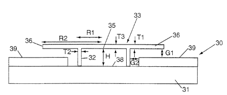
section generally at 30 in Fig. 1. The pressure sensor 30 is formed on a
structural
substrate 31, e.g., glass, to which is attached a deformable sensor structure
comprising a base section 32 (which may be but is not necessarily cylindrical)
and a
flat deformable diaphragm 33. The diaphragm 33 has a central section 35 and an
outwardly extending peripheral skirt section 36. The central portion 35 of the
diaphragm together with the cylindrical walls of the base 32 and a surface 38
of the
substrate 31 define a sealed cavity, which may be evacuated or set at a
reference
pressure. An electrode ring 39, e.g., of a conductive metal such as platinum,
gold,
aluminum, etc., is formed on the substrate 31 under the extending skirt 36.
The
electrode 39 forms one of the plates of a capacitor, a second or stationary
electrode,
with the other plate defining a first or deflecting electrode formed by the
extending
skirt 36 spaced above and adjacent to the electrode 39. For example, the skirt
36
may be coated with an electrically conductive material or the skirt itself may
be
formed of a material, such as single crystal silicon, which is doped to be
electrically
conductive.
As illustrated in Fig. 2, an increase in ambient pressure causes a
downward deflection of the center portion 35 of the diaphragm 33, bringing the
center of the diaphragm closer to the substrate surface 38. This deflection,
in turn,
raises the skirt 36 away from the plates 39. If the pressure increases enough,
the
central portion 35 of the diaphragm 33 will touch down to the surface 38 as
illustrated in Fig. 3. However, because of the manner of the construction of
the
sensor, further increases in pressure continue to result in changes in the
deflection
of the skirt or flap sections 36 away from the plate 39, allowing the pressure
sensor
to continue to detect pressure changes even at such "over-pressure"
conditions.
It is a particular advantage of the pressure sensor structure of the
present invention that the skirt, with its associated electrode, can deflect
away from
the adjacent electrode (e.g., as formed on the substrate) with increases in
pressure.
In conventional capacitive pressure sensor designs, the diaphragm with its
associated electrode is drawn closer to the underlying electrode on the
substrate as
the ambient pressure increases. Consequently, it is generally not possible to
control
the position of the diaphragm by applying a voltage between the electrodes on
the
CA 02341182 2001-02-19
WO 00/11444 PCT/US99/18702
substrate and diaphragm, since such a voltage would tend to draw the diaphragm
toward the substrate. In contrast, applying a voltage between the skirt 36 and
the
underlying electrode 39 tends to draw the skirt toward the substrate, which
can thus
oppose the upward deflection of the skirt as ambient pressure increases. This
feature allows feedback control of the position of the skirt toward a
reference
position, and the level of the voltage applied between the plates to maintain
the
reference position may be used as a signal indicative of the ambient pressure.
To illustrate the properties of the pressure transducer in accordance
with the invention, the following dimensions and displacements, which are
illustrated with respect to Figs. l and 2, may be defined:
T 1 = Thickness of skirt or flap 36;
T2 = Thickness of sidewalk;
T3 = Thickness of central cap 35 on sealed cavity;
R1 = Radius of sealed cavity;
R2 = Radius of diaphragm;
H = Height of sealed cavity;
G1 = Nominal gap between skirt 36 and electrode 39;
G2 = Clearance between electrode 39 and sidewalls of base 32;
D 1 = Deflection at center of diaphragm (downward is negative,
upward positive);
D2 = Deflection at support where diaphragm 33 is attached to base
32; and
D3 = Deflection at peripheral rim of skirt 36.
The following examples illustrate the performance of a pressure
sensor as in Fig. 1. In each example, the parameters T1=T2=T3=Sp,m;
H=30p,m; G1=Sp,m; G2=0; Young's modulus = 160 GPa; residual stress = 20
MPa tensile; and Poisson's ratio = 0.2.
For the first example, in which R1 = 300p,m and R2 = 424~n, Fig.
4 illustrates the calculated deflection versus pressure and Fig. 5 illustrates
calculated
capacitance versus pressure. As shown therein, the deflection of the center of
the
diaphragm terminates as the diaphragm reaches bottom but the displacement of
the
extending skirt, and thereby the relative capacitance between the plates of
the sensor
capacitor, continues to change beyond the point of touch down. Fig. 6
illustrates
3S computed deflection versus pressure and Fig. 7 illustrates computed
capacitance
versus pressure for a second pressure sensor in which R1 = SOOwm and R2 =
CA 02341182 2001-02-19
WO 00/11444 PCT/US99/18702
_g_
707pm. Fig. 8 illustrates computed deflection versus pressure and Fig. 9
illustrates
computer capacitance versus pressure for a third example in which R1 = SOOpm
and R2 = 1000pm. Again, for each of these examples, it is seen that the
capacitance changes with applied pressure in a substantially linear manner up
to
touch-down, but also continues to change in response to additional pressure in
a
repeatable (if nonlinear) manner after touch-down of the diaphragm to the
underlying substrate surface.
The sealed cavity pressure sensor of the invention can be produced
utilizing standard semiconductor processing techniques with fewer masking and
etching steps than are required for other sealed cavity micromachined
capacitive
pressure transducers. Suitable processing techniques are described in the
article by
Yogesh B. Gianchandani and Khalil Najafi, "A Bulk Silicon Dissolved Wafer
Process for Micromechanical Devices," J. of Micromechanical Systems, Vol. 1,
No. 2, June, 1992, pp. 77-85. A processing sequence for producing the pressure
transducer 30 of Figs. 1-3 is illustrated with respect to the views of Figs.
10-13, in
which only three masking steps are required. The first step, as illustrated in
Fig.
10, involves the lithographic masking of a single crystal semiconductor (e.g.,
silicon) substrate 45 and etching using reactive ion etching, or any other
suitable
method, to etch away the substrate in areas 46 adjacent to the structure and
to leave
a central cavity 47 which is surrounded by a relatively thin walled
cylindrical
structure 48 which will constitute the base of the pressure sensor. The next
step, as
illustrated in Fig. 11, is the masking of the regions of the substrate 45 to
define
areas 50 on either side of the cylinder 48 and a boron diffusion step in which
boron
diffuses entirely through the upright cylinder 48 and to a selected depth into
the
substrate 45 in the regions 50 which surround the cylindrical structure 48. It
is
understood that the views of Figs. 10 and 11 are illustrative cross-sectional
views,
and that the regions 50 constitute a region (which may be circular or other
configuration) surrounding the cylindrical structure 48. In a next step, as
illustrated
in Fig. 12, a structural substrate such as a glass wafer substrate 31 has
metal
electrodes 54 and 39 inlaid thereon. The electrodes 54 and 39 are separated by
an
open surface area 55 of the glass structural substrate 31 which electrically
insulates
CA 02341182 2001-02-19
WO 00/11444 PCT1US99/18702
-9-
the electrodes 39 and 54 from each other. The structure shown in Fig. 13 is
immersed in an enchant which etches away the undoped portions of the silicon
substrate 45 to leave the diaphragm 33 defined by the heavily boron doped
portion
of the substrate. The regions 50 are free to now define the extending skirt
sections
36 of the diaphragm and the central portion 35. The freed part is anodically
bonded
to the structural substrate 31, as illustrated in Fig. 13, preferably before
or
alternatively after etching away of the semiconductor substrate 45, with the
electrode 54 in contact with and extending partially, but not entirely,
underneath the
cylindrical wall 32 of the base. The electrode 54 is thus in electrical
contact with
the base 32, and thus with the diaphragm 33 because the base and diaphragm are
heavily doped and therefore are good electrical conductors. The electrode 39
forms
a plate of the capacitor with the extending skirt portions 36 of the
diaphragm.
Although the semiconductor structure is shown in cross-section only in Fig.
13, it is
understood that the electrode 39 would be formed in a pattern surrounding the
base
32 at the electrode 54 (where the electrode 39 terminates so that it remains
spaced
from and electrically isolated from the electrode 54).
Other ways for making contact to the diaphragm or otherwise
providing coupling without requiring connections through the walls of the
sealed
cavity are illustrated in Figs. 14-16. As shown in Fig. 14, connection may be
made
to the diaphragm 33 by a protruding post of heavily doped silicon 60 which
extends
up from contact to an electrode 54 to contact with the diaphragm 33. A notch
may
be formed in the skirt 36 around the post 60 to allow the skirt to flex
freely. In the
structure shown in Fig. 15, a free-standing post of heavily doped silicon 62
extends
upwardly from contact to an electrode 54, with silicon wires 63 extending from
the
post 62 to the edge of the diaphragm 33. In Fig. 16, a first half electrode 39
and a
second half electrode 54 are formed on the substrate 31, with the base 32 and
diaphragm 33 being electrically isolated from both of the electrodes 39 and
54. The
electrodes 39 and 54 are capacitively coupled together through the diaphragm
33,
which thus forms an intermediate conductive sheet in the capacitor defined
between
these two electrodes.
CA 02341182 2001-02-19
WO 00/I1444 PCTNS99/18702
-10-
One way to increase the effective capacitance, and thus the
sensitivity, of the pressure sensor is to reduce the spacing between the
deformable
diaphragm and the electrode 39. Structures in accordance with the invention
which
may be utilized to reduce electrode spacing while maintaining the relative
S dimensions of the structure, particularly the sealed cavity, are illustrated
in Figs.
17-20. With reference to Fig. 17, the substrate 31 is formed with a well or
depression 65 therein which is encircled by the base 32 bonded to the surface
of the
substrate 31. The height of the cylindrical walls 32 can thus be made shorter
while
maintaining the same maximum downward deflection of the diaphragm 35. In Fig.
18, a large depression 66 is formed in the substrate 31 which has a large flat
bottom
67 that is wide enough to receive the entire base 32, and the base is bonded
to the
bottom surface 67 of the depression. In this manner, the total height of the
cylindrical base 32 may be maintained while nonetheless reducing the spacing
between the electrode 39 and the outwardly extending skirt 36. As shown in
Fig.
19, the spacing between the electrode 39 and the extending skirt 36 may also
be
reduced by forming a very thick electrode 39 (e.g., by electroplating onto the
substrate) to a desired height which results in the reduced spacing between
the
electrode and the skirt. As shown in Fig. 20, other substrates 31 may be used,
including a silicon-on-insulator substrate which includes a base layer of
crystalline
silicon 68, an insulating layer of silicon dioxide 69, and a surface layer 68'
of
silicon grown on the oxide layer 69. A depression 65 is formed by etching into
the
surface silicon layer 68' until it reaches the surface 65 of the oxide layer
69. The
base 32 is then bonded on to the exposed surface 65 of the oxide, with a
resulting
reduced spacing between the electrode 39 and the extending skirt 36 of the
diaphragm.
Various other structures may be formed in accordance with the
invention in addition to the cylindrical base topped by a flat diaphragm
structure of
Figs. 1-3. Examples of such structures are illustrated in Figs. 21-28. In the
structure of Fig. 21, a cylindrical base 70 is closed at its top by a
diaphragm panel
71 and has skirts 72 forming the first electrode extending outwardly from the
cylindrical base 70 at an intermediate position more closely spaced to the
second
CA 02341182 2001-02-19
WO 00/11444 PCT/US99/18702
-11-
electrode 39 on the substrate. In the structure of Fig. 22, a cylindrical base
75 is
sealed at its top by a diaphragm 76 that has a downwardly extending portion 77
and
an outwardly extending portion 78 which defines a skirt forming a first
electrode
spaced closely adjacent to the second electrode 39. In both of the structures
of Fig.
21 and Fig. 22, flexing of the diaphragm and the cylindrical sidewalls with
changes
in pressure will cause deflection of the extending skirts 72 and 78 to result
in
changes in capacitance.
In the structure of Fig. 23, a sealed interior cylindrical can structure
80, formed of a base with a diaphragm panel sealed thereto similar to the
structure
of Fig. 21, is surrounded by a closely spaced outer cylindrical structure 81
which
has openings 82 in the top wall thereof. As the walls of the inner cylindrical
can 80
that define the first electrode extend outwardly or draw inwardly with changes
in
ambient pressure, the capacitance between the closely adjacent surfaces of the
inner
cylinder 80 and the outer cylinder 81 {forming the second electrode) changes.
In
the structure of Fig. 24, two sealed cavity structures 85 and 86 formed of a
base
sealed by a diaphragm panel are mounted closely adjacent to each other on the
surface of the substrate 31 separated by a small spacing distance 87. As the
walls
of the structures 85 and 86, which form the first and second electrodes,
expand or
contract with pressure, the closely adjacent walls in these two structures
will deflect
toward or away from each other, changing the capacitance between the
structures.
In the structure of Fig. 25, a base 90 is secured to the substrate 31
and has upwardly extending cylindrical sidewalls 91 and outwardly extending
skirt
sections 92 forming a first electrode which are spaced above the second
electrode
39. A sealed cavity in this case is formed by securing a further diaphragm
structure
93 to the top of the skirt sections 92. As the diaphragm 93 is, for example,
pushed
downwardly by increasing pressure, the skirts 92 will be drawn upwardly away
from the electrode 39, thereby changing the capacitance between these
structures.
The structure of Fig. 25 is adapted for production by a surface micromachining
process using typical micromachined materials, e.g., polysilicon.
In the structure of Fig. 26, two sealed, spaced cavity structures 97
and 98, formed of a base sealed by a diaphragm, are mounted to the substrate
31
CA 02341182 2001-02-19
WO 00/11444 PCT/US99/18702
-12-
above a single second electrode 39 and have a bridge skirt section 99 between
them
forming the first electrode, which is suspended above the second electrode,
and
which may be perforated with openings 100. The structures 97 and 98 may be a
single semi-annular cavity to ensure that the pressures in the two sides of
the
cavities are the same. As the walls of the sealed cavity structures 97 and 98
expand
outwardly or contract inwardly with changes in pressure, the thin bridge skirt
99
between them will bulge upwardly or downwardly to change the effective
capacitance with respect to the electrode 35.
In the structure of Fig. 27, a cylindrical base 105 is bonded to the
surface of the substrate 31 and has outwardly extending skirts 106. Instead of
a flat
diaphragm, the diaphragm is formed with a conical form 107. As the surfaces of
the conical section 107 are pushed inwardly with increasing pressure, the
skirt
portions 106 forming the first electrode are rotated upwardly away from the
second
electrode 39 to change the capacitance, and vice versa with a decrease in
external
pressure.
In the structure of Fig. 28, a hemispherical base 110 defining a
continuous base and diaphragm structure is bonded to the substrate 31 to form
a
sealed cavity 111. A skirt 113 forming the first electrode extends out from
the base
110 over the second electrode 39 in close proximity thereto. As the domed
structure 110 deflects inwardly under increasing pressure, the skirt section
113 is
rotated away from the electrode 39, and vice versa with a decrease in
pressure.
It is understood that the invention is not confined to the particular
construction and arrangement of parts set forth herein for illustration, but
embraces
such modified forms thereof as come within the scope of the following claims.