Note: Descriptions are shown in the official language in which they were submitted.
CA 02341212 2001-02-19
WO 00/14928 PCT/US99%18293
MULT1-PART PACKET PROCESSOR
This application claims the benefit of U.S.
provisional Application No. 60/057,813, filed September 4,
1997, which is incorporated herein by reference.
BACKGROUND OF THE INVENTION
This invention relates generally to a computer
network, and in particular to a multi-port packet processor
for processing communication within a computer network.
A computer network is an interconnection of various
computers by a network of communication devices (often
utilizing more than one communications protocols). One such
example of a computer network is the Internet that
interconnects personal computers and servers through
telephone lines and high-speed transmission lines. Other
examples of computer network include a local area network
(LA~'1), a wide area network (wAN), and other special purpose
net~~rorks including net~.~orks based upon protocols such as RS-
485 instrumentation protocol and Universal Serial Bus (USB).
2~ The interconnection o. (relatively) smaller devices into a
neterork facilitates transactions of large scale
organizations, allows for efficient dissemination of
information, provides for communications between various
devices within the network, and allows for sharing of
resources and data.
Fig. 1 illustrates a conventional computer network
100. Network 100 includes a number of user computers 110 and
servers 112 interconnected'together through hubs 120,
switches 122, and a router 124. The user computers 110 and
servers 112 connect to the network through respective Network
Interface Cards (NICs, not shown). The NICs receives data
(i.e., in pytes) from the computer or server and =orms data
packets for transmission on the net~~ro~k transmission line.
The hubs,_switches, and routers receive the data packets and
~0 direct the packets to the proper destination. At the
SUBSTITUTE SHEET (RULE 26)
CA 02341212 2001-02-19
WO 00/14928 2 PCT/US99/18293
destination, another NIC receives the data packets and
translates the packets into bytes usable by the computer or
server. The interconnection between a pair of devices can be
an Unshielded Twisted-Pair (UTP) cable (such as a telephone
line), a coaxial cable, a fiber optic cable, or other
transmission mediums.
A network can be viewed as being composed of
various layers, with each layer performing a defined
function. Each layer communicates with the layer above
and/or below it. Furthermore, each layer can be implemented
with hardware or software, or a combination of both.
Fig. 2 illustrates the variaus layers of an Open
System Interconnection (OSI) computer network 200. Computer
network 200 is composed of seven layers including: (1) a
physical layer 210, (2) a data link layer 212, (3) a network
layer 21~, (4) a transport layer 216, (5) a session layer
218, (6) a presentation layer 220, and (7) an application
layer 222. The physical layer 210 transmits bit streams
across the physical transmission system. The data link layer
212 provides for a reliable data transmission. The network
layer 214 routes data from one network node to another. The
transport layer 216 provides data transfer between two users
at a predetermined level of auality. The session layer 218
manages the data exchange. The presentation layer 220
presents information to the users in a meaningful manner.
Finally, the application layer 222 monitors and manages the
computer network 200.
Communication between the various layers is
governed by a set of protocols. The layers and protocols, in
turn, define the architecture of a network. Conventionally,
many diverse protocols exist that are incompatible with other
protocols. Some protocols are adopted by large manufacturers
to differentiate their products from those of other
manufacturers, or for other reasons. Thus, although a
product from one product line can communicate with other
products from the same product line, it is often incompatible
with other products from other manufacturers. Examples of
network protocols include Integrated Services Data Netcaork
(ISDN), Ethernet, Fast Ethernet, Gigabit Ethernet,
SUBSTITUTE SHEET (RULE 26)
CA 02341212 2001-02-19
WO 00/14928 PCT/US99/18293
3
Asynchronous Transfer Mode (ATM), Copper Distributed Data ---
Interface (CDDI), Fiber Distributed Data Interface (FDDI) and
Fiber Channel (also known as P1394).
Interconnectivity and interoperability between
(compatible and incompatible) networks, or segments of a
network, can be provided by interconnection devices (e. g.,
routers, hubs, bridges, gateways). With the proliferation of
networks in the marketplace, and the numerous protocols in
used, the interconnection devices become an integral part of
many networks. Referring to Fig. 2, a hub 230, which
operates on the physical layer 210, is used to connect
segments of the same network to form an extended network. A
hub is also referred to as a repeater. A bridge 232, which
operates on the data link layer 212, is used to connect
compatible (or nearly compatible) LANs. A router 234, which
operates on the network layer 214, connects two network
segments to form one large network. Finally, a gateway 236,
which operates on any layer at or above the~network layer
214, connects an internal network to an external network.
The gateway 236 is the most complex but also most flexible
interconnection device, as it allows for different protocols
at any or all layers on which it operates.
As networks become larger and faster, new
applications requiring greater bandwidth become feasible.
Examples of high bandwidth applications include video on
demand, video games, and others. These applications place
stress on various parts of the network architecture,
including the NICs, the communications channel, and the
interconnection devices (e.g., the servers). A bottleneck is
often created in the data communications system, with one
likely area of congestion being the main computer bus of the
server.
From the above, it can be noted that a processor
that facilitates high-speed data communications is,needed.
SU~li~IA.Ry OF THE INVENTION
According to the invention, a mufti-port packet
processor provides an efficient mechanism to interface
multiple high-sped packet-based communications channels to
SUBSTITUTE SHEET (RULE 26)
CA 02341212 2001-02-19
WO 00/14928 PCT/US99/18293
4
each other. The mufti-port packet processor is implemented
within an integrated circuit for low cost, high performance,
and improved reliability.
The mufti-port packet processor includes m~:ltiple
port processors. Each port processor can include a channel
interface for coupling to a respective communications channel
and a channel processor for processing the packets received
through the channel interface. The channel interface can be
designed to process packet-based communication from a channel
using a particular set of packet-based protocols.
Alternatively, the channel interface can be designed having
programmable control such that the channel interface can be
configured to send and receive packets using a selected set
(from a number or possible sets) of packet-based protocols.
Each port processor can further include an
interprocessor communications interface coupled to at least
one other port processor for providing communication between
the port processors.
In a specific embodiment, the port processor is
capable of processing multiple communications channels
concurrently. The communications channels can have identical
packet-based protocols or different packet-based protocols.
The mufti-port packet processor can be used in a
variety of applications. In one application, the mufti-port
packet processor functions as a local area network (LAN)
processor and provides the functions typically provided by a
LAN server. In another application, the mufti-port packet
processor functions as a disk storage processor and manages
data transfer between various storage devices.
The invention will be better understood by
reference to the following detailed description with
accompanying drawings.
BRIEF DESCRIPTION OF TBE DRAWINGS
Fig. 1 illustrates a conventional computer network.
Fig. 2 illustrates various layers or an Open System
Interconnection (OSI) computer network.
Fig. 3 is a simplified block diagram illustrating a
local area network (LAN) channel communications hub.
SUBSTITUTE SHEET (RULE 26)
CA 02341212 2001-02-19
WO 00/14928 PCT/US99/18293
Fig. 4A is a block diagram of one embodiment of an
integrated multi-port processor.
Fig. 4B is a block diagram of another embodiment of
an integrated multi-port processor.
5 Fig. 4C is a block diagram of yet another
embodiment of an integrated multi-port processor.
Fig. 5 shows a specific application wherein a
multi-port processor is used to process data transfer in a
mass storage environment.
Fig. 6 shows another specific application wherein a
more than one of multi-port processors are configured as a
two-dimensional grid packet server.
Fig. 7 shows yet another specific application
wherein a more than one of multi-port processors are
configured as a three-dimensional grid packet server.
DETAILED DESCRIPTIO~1 OF SPECIFIC EMBODIMENTS
L.~~1 H a b
Fig. 3 is a simplified block diagram illustrating a
local area network (L~~1) channel communications hub 300. LuIN
hub 300 includes a number of packet-based protocol channels
310 coupled to a multi-port processor 320. L.~cV hub 300 can
correscond to hub 120 in the network sho4m in Fig. 1.
Channels 310 (sho~.~n symbolically as blocks in Fig. 3) include
different LP.N channels such as ISDN, Ethernet, Fast Ethernet,
Gigabit Ethernet, ATM, CDDI, FDDI, or P1394 (also known as
Firewire) channels, or other communications channels.
Furthermore, the various channels 310 shown in Fig. 3 may
utilize different types of protocols. For example, some
channels 310 may support mass storage communications
protocols (e. g., Small Computer Systems Interface SCSI) while
other channels 310 may support LAN protocols (e. g.,
Ethernet).
Multi-Port Processor
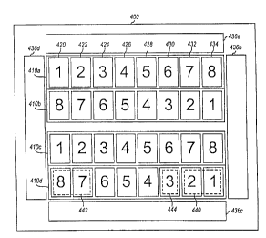
Fig. 4A is a block diagram of one embodiment of an
integrated multi-port processor 400. Multi-port processor
400 can operate as multi-port processor 320 in Fig. 3.
SUBSTITUTE SHEET (RULE 26)
CA 02341212 2001-02-19
WO 00/14928 PCT/US99/18293
6 -
Multi-port processor 400 efficiently controls and manages
communication through multiple packet-based protocol channels
310. Conventionally, this function is performed by a larger
device, such as a LAN server.
Multi-port processor 400 includes a number of port
processors 410. In an embodiment shown in Fig. 4A, there are
four port processors 410 and each part processor 410 includes
eight circuits. The eight circuits include: (1) input/output
(I/O) buffers 420, (2) I/0 controllers 422, (3) an
interprocessor communications circuit 424, (4) a channel
processor 426, (5) a cache controller 428, (6) an internal
memory 430, (7) a memory controller 432, and (8) memory
buffers 434. Each of the circuits is further discussed
below.
I/0 buffers 420 provide buffering of data packets
received from, and to be transmitted on, the communications
channel. I/O controllers 422 direct reception and
transmission of the data packets and can include a temporary
storage element for queuing packets and performing data
processing tasks such as encryption/decryption, format
conversion and error correction/detection operations upon the
data of one or more packets.
Inter~rocessor communications circuit 424 can
include an interrupt controller for triggering specific real-
time actions in response to either network conditions, higher
level net<<~ork control commands, or other port processors and
an interprocessor I/O circuit. The interprocessor I/O
circuit can include clock timer counters and other circuits.
Channel processor 426 directs the operation of port
processor 410 and can be implemented as a microprocessor, a
microcomputer, a microcontroller, an applications specific
integrated circuit (ASIC}, a digital signal processor (DSP),
a finite state machine (such as a register store, Field
Programmable Gate Array-FPGA, or Complex Programmable Logic
Device-CPLD), or similar circuits. Cache controller 428 can
include a cache (i.e., a first level cache). Internal memory
430 provides storage for data and program codes and can be
implemented as a random-access memory (RAM), a dynamic
random-access memory (DR.AM) , a read-only memory (ROM) , a
SUBSTITUTE SHEET (RULE 26)
CA 02341212 2001-02-19
WO 00/14928 PCT/US99/18293
FLASH memory, other similar devices, or a combination of the-
above. Additionally, internal memory X30 can include a boot
ROM (or possibly a boot FLASH memory) for initializing port
processor 410. In one embodiment, internal memory 430 can
include enough memory (i.e., enough RAM, ROM, and other
memories} such that an external memory is not required.
Memory controller 432 directs the exchange of data between
port processor 410 and an external memory. Memory buffers
434 provides buffering of data received from, and to be
transmitted to, the external memory.
As shown in Fig. 4A, multi-port processor 400
further includes a support circuit 436 for each port
processor 410. In particular, support circuits 436a, 436b,
436c, and 436d couple to port processors al0a, 410b, 410c,
and 410d, respectively. Support circuit X36 can include I/O
circuits, a memory, drivers, and other circuits. Support
circuit =.36 facilitates communication between port processor
410 and the one or more communications channels associated
with the port processor. Support circuits 436 can provide
analog conversion for different physical signal states .
communicating bits on the coupled communication cannel. For
example, this analog conversion can transform logic signal
(e.g., for zero and one) to drive a laser which requires a
different signaling convention.
Communication Mechanisms
Referring to the embodiment shown in Fig. 4A, each
port processor 410 includes three communications mechanisms:
(1) a channel interface 440, (2) an external memo-~-y interface
442, and (3) an internal processor (or interprocessor)
communications interface 444. Channel interface X90 includes
I/O buffers 420 and I/O controllers 422. External memory
interlace 442 includes memory controller 432 and memory
buffers 434. Interprocessor communications inter_ace 444
includes interprocessor circuit 424.
Channel interface 440 can be designed to process
packet-based communication from a channel using a particular
set of racket-based protocols. Alternatively, channel
interface 440 can be designed having programmable controls
SUBSTITUTE SHEET (RULE 26)
CA 02341212 2001-02-19
WO 00/14928 PCT/US99/18293
g
such that the channel interface can be configured to send and
receive packets using a selected set (from a number of
possible sets) of packet-based protocols. The
programmability can be provided by impleme.zting channel
interface 440 (i.e., I/O controller 424) with a processor, a
finite state machine, or other suitable devices. The
processor or finite state machine can be designed with the
capability to initiate and operate using one of various sets
of states. Such processors or finite state machines may
either be fixed program or reconfigurably programmable.
An interprocessor communications network is made up
of multiple interprocessor communications interfaces 444.
The interprocessor communications network can interconnect
all port processors 410, or a subset of port processors 410.
Furthermore, the interprocessor communications network
includes a communications mechanism that can include packet
data transfer and (possibly) transfer command/status signals.
The interprocessor communications network allows
the various port processors 410 to coordinate and efficiently
manage communication between two or more communications
channels. For e:cample, one port processor 410 may be
assigned to one channel utilizing a particular set of
protocols and another port processor 410 may be assigned to
another channel utilizing the same or a different set of
Drotocols. The interprocessor communications n~t~.rork allows
for communication between two (possibly incompatible)
channels. In this manner, the interprocessor communications
network behaves like bridge 232 or routes 234 as shown in
Fig. 2.
Note the shape of the port processors ~10a, 410b,
410c and 410d. The circuits are shown as roughly
rectangular, which is the approximate shape they ~rould
possess in an integrated circuit layout. The individual
components of the port processors would not necessarily be
approximately the same size, but are sho~,rn this ':;ay for
diagrammatic convenience. The individual components of the
port processors vrould however be approximately rectangular.
Further note the arrangement of the port processors
410a, 410b, 410c and 410d. They are arranged so that the
SUBSTITUTE SHEET (RULE 26)
CA 02341212 2001-02-19
WO 00/14928 PCT/US99/18293
9 - _ _
long axis orientation is flipped for neighboring port
processors. Preferred embodiments include pairs of port
processors sharing the same orientation and neighboring pairs
being flipped. Another preferred embodiment where the port
S processors do not possess external memory interfaces include
only two groups of port processors in one integrated circuit,
where each group shares an orientation and one group's
orientation is flipped from the other group's orientation.
Further note the placement o~ the interprocessor
communications interface 444. These circuits are optimally
placed within the port processor so as to minimize the total
wire length required. Accomplishing this requires knowledge
of which port processor arrangements are to be implemented.
Where there is to be orientation flipping, either the
placement should be essentially in the middle of the part
processor rectangular shape, or it should be split into two
components, c~hich are located at appro:cimately equal
distances from the center of the port processor long axis.
Port Drocessina
In one embodiment, each port processor 410 has the
capability to simultaneously interface with one or more
packet-based protocol channels. High-speed packet transfers
bet<<reen these channels by one port processor 410 are
accommodated by the channel interface communications
mechanism (i.e., provided by I/O buffers 420 and I/0
controllers 422) within that port processor 410. This
transfer activity is controlled by the corresponding channel
processor 426 within that port processor. 410. This provides
for an efficient, low overhead transfer mechanism between the
"local" channels within each port processor 410.
In another embodiment, communication between
channels coupled to different port processors 410 is provided
by the interprocessor communications network. In this
embodiment, packat data transfers proceed unimpeded while
command and status transactions occur concurrently. Packet
data transfer occurs on physically separate channels from
command and status information transfers. Neither is slowed
by the transfer characteristics of the other.
SUBSTITUTE SHEET (RULE 26)
CA 02341212 2001-02-19
WO 00/14928 PCT/US99/18293
_ _ -
Port processor 410 can be designed to operate on
one or more layers (similar to the design of gateway 236).
Referring to Fig. 2, port processor 410 can be designed to
operate on physical layer 210, data link layer 212, network
5 layer 214, or a combination of these layers.
Packet transfer and conversion can be partitioned
into separate component activities of block data transfer and
block data processing. These separable activities are
preferably performed by distinct concurrently operating
10 mechanisms, which by and large do not interfere with each
other. The block data transfer is further preferably
isolated from disruptive intrusions caused by the
communication of control and status information through the
use of separate communications mechanisms for such
activities.
Modular Design
Fig. 4B illustrates the flexibility in the design
of a multi-port processor because or the modular design of
the port processor. A multi-port processor 402 can interface
and process data transmissions using various packet-based
protocols. Alternatively, a multi-port processor 402 may
interface and process just one data transmission using just
one pac'.,et- -based protocol. As shown in Fig. 4B, port
Drocessors 412a, 412b, 412c, and 412d include channel
interfaces 450a, 450b, ~5oc, and 450d, respectively. Each
channel interface 450 can be designed with a particular set
of I/O bu~fers and I/O controllers corresponding to the
packet-based protocols to be utilized. Alternatively, as
described above, each channel interface 450 can have
programmable controls to allow processing of packets using a
selected set of protocols from among a number of sets of
protocols. For example, one channel interface 450 of multi-
port processor 402 can support ISDN or Ethernet, another
channel interface 450 can support ATM, and another channel
interface 450 can support SCSI. As another example, a four
port multi-port packet processor can include one Gigabit
Ethernet port processor, one Fast Ethernet port processor,
SUBSTITUTE SHEET (RULE 26)
CA 02341212 2001-02-19
WO 00/14928 PCT/US99/18293
11 - ----
one Ethernet port processor, and one Fiber Channel port
processor interfacing to a disk farm.
Fig. 4C is a block diagram illustrating a multi-
port processor 404 including six port processors 410. Multi-
port processor 404 is different in configuration than multi-
port processor 400 (see Fig. 4A) which includes only four
port processors 410. As these examples show, the multi-port
processor can be designed to include any number o~ port
processors, including two, four, six, eight, sixteen, thirty-
two, or any other number. Although an even number of port
processors can provide certain advantages (e. g., layout
efficiency), odd number of port processors can also be
designed and utilized. Again, as described above, each port
processor 410 can include a different channel interface
(i.e., diff°.rent set of I/0 buffers and I/O~controllers) or a
programmable channel interface.
Referring to Figs. 4A through 4C, each Dort
processor is shown having a single channel interface.
However, a port processor can be designed to include any
number channel interfaces. Furthermore, each port processor
can be designed with a channel interface without regards
(i.e., individually and independently) to the other port
processors within the multi-port processor. For e:{ample, a
multi-port processor can be designed such that one port
processor includes one channel interface, a second port
processor includes two channel interfaces, a third port
processor includes three channel interfaces, and so on.
Examples of this include multiple RS-485 channels support
GPIH instrumentation protocols and dual USB channels.
O_th~r ADnlications of Multi-port Processor .
Fig. S shows a specific application wherein a
multi- -port processor 500 is used to process data transfer in
a mass storage environment. This environment is commonly
referred to as a "disk farm". The disk farm includes a
number of storage devices (e. g., hard disk drives, tape
drives, CD drives, floppy disk drives, or other storage
devices). Each storage device couples to multi-port
processor S00 through a respective communications channel 510
SUBSTITUTE SHEET (RULE 26)
CA 02341212 2001-02-19
WO 00/14928 12 PCT/US99/18293 ,
or 512. An example of a disk farm is a Redundant Disk RAID-
system that provides mass disk storage with a level of
redundancy for increased system reliability. Conventionally,
this data transfer control requires a complex device.
Fig. 6 shows another specific application wherein a
more than one of multi-port proce~~sors 600 are configured as
a two-dimensional grid packet server 610. Fig. 6 shows a
four by four grid of multi-port processors 600. However,
other dimensions can also be used, and symmetry is generally
not required. In one embodiment, a portion of the packet-
based communications channels of each multi-port processor
600 is used for communication in the row and column in which
the particular multi-port processor 600 is located. These
channels may have different protocols. For example, one
channel may employ the PI394 protocol to provide higher
bandwidth within server 610. The remaining channels can be
used for providing communication with the network.
Fig. 7 shows yet another~specific application
wherein a more than one of multi-port processors 700 are
configured as a three-dimensional grid packet server 710.
Fig. 7 sho~.~s a four-by-four-by-four grid of multi-port
processors 700. However, other dimensions can also be used
and symmetry is again generally not required. In one
embodiment, a portion of the packet-based communications
channels of each multi-port processor 700 is used for
communication in the row, column, and quadrant in which the
particular multi-port processor 700 is located. These
channels may have different protocols.
The structures shown in Figs. 6 and 7 can be
extended to a four-dimensional array of multi-port
processors, a five-dimensional array of multi-port
processors, or. an M-dimensional array of multi-port
processors, ~~rhere M is any integer.
The~previous description of specific embodiments is
provided to enable any person skilled in the art to make or
use the present invention. The various modifications to
these embodiments will be readily apparent to those skilled
in the art, and the generic principles defined herein may be
applied to other embodiments without the use of the inventive
SUBSTITUTE SHEET (RULE 26)
CA 02341212 2001-02-19
WO 00/14928 PCT/US99/18293
13 _ __
faculty. For example, each port processor can include
different circuits than that shown in Figs. 4A though 4C,
depending on the functionality required. Thus, the present
invention is not intended to be limited to the embodiments
shown herein but is to be accorded the widest scope
consistent with the principles and novel features disclosed
herein and as defined by the following claims.,
SUBSTITUTE SHEET (RULE 26}