Note: Descriptions are shown in the official language in which they were submitted.
CA 02341218 2001-02-19
1
Contact element
Specification:
The invention relates to a contact element for supplying electric current to
substantially board-
shaped objects that are to be treated by an electrolytic process and to a
contact organ for said
objects which comprises at least one stem and at least one contact element,
the at least one
contact element being arranged at one end of the stem which is bent at an
angle of about 90° and
the stem being movable together with the contact element by means of a
restoring force so that
the contact element can be pushed onto the objects. The invention also relates
to a method of
supplying electric current to the objects. The contact organ is specifically
used in
electrochemical processing plants.
To submit objects to an electrolytic treatment, they have to be transported
and placed in electric
contact in order for them to be supplied with electric current while being in
contact with a liquid
for treatment.
Various appliances are used to serve this purpose. US-A-4,767,146 for example
discloses
holding tongs for printed circuit boards which comprise two legs provided each
with two
gripping arms. On account of the force of a spring, the legs with the gripping
arms are pivotal
about an upper axis, the lower ends being thus pushed together. The lower ends
of the gripping
arms are provided with teeth. The arms of the one leg are provided with two
tooth-Iike
projections each and the arms of the other leg with one tooth-like projection
each.
This contacting and holding appliance is used in conventional electrolytic
tank plants in which
the printed circuit boards are vertically held and dipped into the tank.
Another method consists in conveying the objects through the various
processing stations in
CA 02341218 2001-02-19
2
horizontal direction.
DE 25 12 762 B2 suggests using electrical contact springs for contacting
objects to be
chromium-plated that are fastened on work holding fixtures. For this purpose,
the objects are
clamped in the contact springs which are formed by two springable bars.
For some time past, employment has been made of coating lines for the
electrolytic treatment of
board-shaped objects, in particular for printed circuit boards, the boards
being transported
through said coating plants in horizontal direction. For this purpose the
boards are contacted
with the liquid for treatment, with a galvanizing bath or with a solution
suitable for electrolytic
pickling for example. In order to allow electric current to be supplied to the
boards, appropriate
contact elements are provided. The boards are moreover led through the plant
by conveying
facilities.
Furthermore, WO 97/37062 A1 describes a device for the electrochemical
processing of
electrically conductive areas which are insulated against each other on
printed circuit boards. To
make electrical contact with these areas, brushes are used, whose thin
conductive fibers make
electrical contact with the structured surfaces to be treated. The printed
circuit boards are guided
past the stationary brushes in horizontal direction and in horizontal
orientation so that the tips of
the brushes graze the surfaces. This device is not suited for transmitting
large electric currents
to the printed circuit boards. It is also difficult to find a solution for
practical operation that, on
one hand, provides the brushes with a long working life and that, on the other
hand, protects the
surfaces of the printed circuit boards against damage.
DE 36 45 319 C2 discloses an array for the electrolytic treatment of board-
shaped objects such
as printed circuits. In this array, the printed circuits are conveyed in
horizontal direction and in
horizontal orientation while being held by clamps which are used as conveying
and contacting
facilities. The clamps each consist of two bars which, under the pressure of
the spring, are
pivoted about their mutual, electrically conductive connecting or contacting
point in such a
manner that their lower ends are pushed against one another, thus grasping the
side edge
(galvanoedge) of the printed circuit boards. In practice, the width of the
edge amounts to 10 to
CA 02341218 2001-02-19
3
15 mm. Each printed circuit board is typically contacted on at least one side
by way of several
clamps.
In practical operation, the flow of current is progressively increased in
these plants in order to
accelerate the electrolytic treatment of printed circuit boards. Nowadays,
typical values for the
flow of current already range from 20 to 80 A for every printed circuit side
and clamping contact
when the distance between the clamps amounts to 60 mm for example. The
currents supplied to
one whole printed circuit side by means of several clamps are considerably
larger.
If, for the electrolytic treatment of printed circuit boards coated with
copper on both sides,
clamps that grasp both sides and supply electric contact are used, one such
clamp carries 40 to
160 A. Such large currents are difficult to be transmitted onto the thin
conductive base coating
of the boards. Large currents cause the metal ions in the vicinity of the
contacts to deplete in the
electrolyte so that the deposited coating of metal scorches in the
neighborhood of the contacting
spots on the printed circuit boards (= formation of metal coatings with a
granular crystal
structure).
It has also been observed that the occurrence of the presented phenomena
increases when a base
coating of copper having a reduced coating thickness is electroplated. For
various reasons it is
necessary to reduce the coating thickness from hitherto 17 ~m to at present 6
~m and even to
0.7 ~m for example (when using certain manufacturing techniques ISBU-technique
=
Sequential-Build-Up~, e.g., when fine bores (100~m and less) must be drilled
with laser light or
in order to avoid undercut when thicker base coatings of copper are used, as
well as for reasons
of material saving and to optimize the electric properties of the boards.
These increasing demands placed on the modern fabrication of printed circuits
are no longer to
be met with the devices of the art. The base coatings of copper proved to
"scorch" on the
contacting spots and in the adjacent regions thereof on the surfaces of the
printed circuit boards.
This means that large black spots form at these places, where the copper
coating is damaged or
in parts even completely destroyed. These damages or destructions are in parts
limited to the
areas in which no strip conductor structures are intended to be formed on the
printed circuit
CA 02341218 2001-02-19
4
material. However, these damaged spots are often so large that the border
areas of the strip
conductor structure are damaged as well. In this case, the processed board has
necessarily to be
scrapped. What is particularly disturbing with these scorched spots is that
the residues of
scorching (fine oxidized copper) are in parts lying loose on the board and are
distributed by the
flow of the electrolyte over the surface of the board where they are
incorporated in the coating
on deposition of the metal. As a result, the board is rendered unsuitable for
use.
For reasons of economy, the width for the galvanoedge is desired to be
steadily reduced while
the current density should increase and the thickness of the base layer of
copper be lowered,
which entails the above mentioned problems.
The basic problem of the invention is therefore to avoid the drawbacks of the
devices and
methods of the art and in particular to advance means for achieving a
satisfactory electrolytic
treatment utilizing very large currents while potential impairments of the
metal coating on the
surface of the board are merely tolerated in a very narrow border area and the
above mentioned
requirements can be met even on using very thin layers of copper on the
boards.
The solution of the problems indicated herein above is given by the inventive
contact element
according to claim 1, the contact organ according to claim 14 and the method
of supplying
electric current according to claim 17.
The contact element serves for supplying electric current to objects which are
substantially
shaped like boards, such as printed circuit boards, and which are intended to
be submitted to an
electrolytic treatment in so-called horizontal plants in which the printed
circuit boards are
conveyed in horizontal direction and are oriented either substantially
horizontally or
substantially vertically. The electrolytic processes of interest are
electrolytic metal deposition
and electrolytic pickling as well as other types of electrolytic processes
such as for example
electrolytic purification.
The contact element is provided with one or more contact areas, the shape of
the contact areas
being configured in such a way that no damages occur in the areas of the
copper surface adjacent
CA 02341218 2001-02-19
to the contact areas when large currents are transmitted from the contact
element printed on the
contact areas on the electrically conductive surface to the copper surface.
The large currents may
be transmitted to copper surfaces of printed board materials as well as to
surfaces made from tin,
tin-lead alloy or from another electrically conductive material.
The contact organ according to the invention is provided with at least one
stem and with at least
one contact element. The contact element is arranged at one end of the stem.
The end of the
stem may be bent at an angle of about 90° with respect to the stem. The
orientation of the stem
may also be straight. The stem is movable with the contact element by way of a
restoring force
in such a way that it may be printed onto the surface of the objects. In a
preferred embodiment,
the contact organ consists of two such stems, each of them being bent at an
angle of
approximately 90° at its lower end One contact element according to the
invention is fastened
to each of the bent ends. The two stems are relatively slidable in such a
manner that the opposite
contact elements may be moved toward each other or away from each other. The
two preferably
plane contact areas are arranged so as to be congruent when the clamp is
closed. The areas are
preferably pushed against each other by the force of the spring.
The method according to the invention serves for supplying electric current to
the board-shaped
objects, at least one current-carrying contact element according to the
invention being printed on
the surfaces of the objects, thereby generating a flow of current between the
contact elements
and the objects.
The contact element according to the invention permits to henceforth transmit
even large
currents of 40 to 160 A for example to the printed circuit boards by means of
one single contact
organ of the invention which is provided with at least one such contact
element. As contrasted
with the methods utilizing the conventional contact elements, the surface
areas of the copper
which are printed on the contacting spots on the surfaces of the objects to be
processed are not
damaged even when very large currents are utilized. Thus, a current of, e.g.,
60 A, and of course
a current of less than 60 A as well, can be transmitted to the copper surfaces
of a printed board
material plated with a copper coating of 6 ~m for example, without having the
surface areas
adjacent to the contacting spots noticeably damaged, e.g., worn off while
forming a black
CA 02341218 2001-02-19
6
cinder. On utilizing still thinner coatings of copper on the printed board
material, e.g., coatings
of a thickness of 0.7 pm for example, the problems mentioned may occur with
considerably
smaller currents when using the devices of the art. With the contact elements
in accordance with
the invention the damage described on these materials cannot even be observed
with a flow of
current of 40 A for example.
On examining with care the problems occurring with the prior art devices, it
could be observed
that the contacting spots on the surfaces of the printed circuit boards were
in parts greatly
damaged or completely destroyed. In some cases even, the resin layers of the
base material lying
underneath the copper coating were laid bare and partially blackened and
damaged. In most
cases, the damages were not limited to the very contact areas, they rather
extended over greater
areas so that the surface areas of the printed circuit boards in which the
land patterns would have
had to be formed were damaged as well.
These observations led to the assumption that despite the surrounding liquid
for treatment, the
material, at its border area between the contacting spot on the surface of the
printed circuit board
and the contact spot on the contact organs, on the clamps for example, is
carried to a high
temperature while current is being passed through, thus bringing about the
damages mentioned
With the conventional contact organs, the generated heat could not be
dissipated efficiently with
appropriate expenditure. Since the contact organs have to be made of a
chemically very resistant
material, titanium is preferably used. This material has the disadvantage that
its thermal
conductivity is bad It is not possible to have copper, which has a better
conductivity,
substituting for titanium, due to the want of chemical resistance of copper
since copper
disintegrates during the subsequent stripping process conducted on the clamps.
Improvement was obtained by increasing the force used to print the contact
spots on the surfaces
of the printed circuit board. In so doing, the damages mentioned to occur to
the layer of copper
and to the insulating material could be reduced. The increased forces however
made it difficult
to open and close the contacts, so that this solution proved to be
unsatisfactory. Customary
contact forces are of 10 to 30 N. Furthermore, on account of the existing
tendency to reduce the
coating thickness of copper on the outer sides of the printed circuit boards,
the contact force
CA 02341218 2001-02-19
7
cannot be increased ad lib. Very thin copper layers in particular, such for
example having a
thickness of 0.7 ~,m, are very sensitive and are damaged or destroyed, thereby
possibly shorn
off, by very large contact forces. As a result thereof, the flow of current is
hampered or even
interrupted
The solution found out to eliminate the foregoing problems involves increasing
the contact area
of the contact spots. This approach is only successful though when the area
available on the
galvanoedge is large enough. On account of the now existing tendency to keep
its width as small
as possible in order to minimize this useless area portion of the printed
board material, this
alternative proved to be unsuitable for execution.
In a manner in accordance with the invention, by contrast, the length of the
boundary line
between the contact areas of the contact elements, the corresponding
contacting areas on the
board-shaped objects and the surrounding liquid for treatment is increased
relative to the contact
area.
Therefore, contact elements according to the invention are preferably provided
with contact
areas which are limited by boundary lines, the shape of the contact areas
being designed in such
a way that the ratio V of the square of the overall length L of all boundary
lines to the size F of
all the contact areas
L2
Y=-
F
is at least 25, preferably at least 30 and in particular at least 35. The
contact areas are preferably
essentially plane.
The boundary line delimits a contact area which is preferably essentially
plane. It demarcates at
the same time the transition of the contact element to the surrounding liquid
for treatment and
to the surface of the object on which the contact element is printed. When
using contact
elements whose contact areas pass over to the lateral areas via rounded edges,
the boundary
CA 02341218 2001-02-19
g
lines are determined by the transitions between the contact element, the
liquid for treatment and
the surface of the object. In this case too, the boundary lines constitute the
outer demarcation of
the preferably substantially plane contact areas.
The contact element may be provided with at least two humps for example which
are separated
by intervals and which have one contact area each, said contact areas being
preferably
substantially plane (two-dimensional). The contact areas lie substantially in
one plane and are
arranged in such a manner that electrical contact can be made among all the
contact areas and
their corresponding contacting areas on the printed circuit boards. To this
purpose the contact
areas are customarily printed on the galvanoedge of the printed circuit boards
by means of a
contact force.
In another preferred embodiment the contact element may be provided with at
least one contact
area, the preferably substantially plane contact area assuming a shape which
is an appropriate
variation of simple two-dimensional geometric figures for prolonging the
boundary line as
compared to the boundary line in a conventional contact element. The contact
area can be star-
shaped, trifoliate or dumbbell-shaped Other shapes having a prolonged boundary
line are
conceivable, irregular shapes for example. Such two-dimensional shapes are
preferably provided
with bight portions on their periphery. The periphery may also be provided
with notches
resembling saw teeth for example.
The inventive embodiments of the contact element have the advantage desired.
The reason why
this is so is not known, though. But it has been assumed that the selected
arrangement allows
better cooling of the contact spots and a more uniform supply of large
currents, to very thin
layers of metal in particular. On account of the longer boundary line, the
current density flowing
at the transition between the contact spots and the work is lower. Normally,
the current flowing
through the contact spots on the surfaces of the printed circuit boards
considerably heats the
material. It is possible that it is this rise in temperature that occasions
the damage or destruction
caused to the printed board material. By having the inventive contact elements
provided with
several humps fitted with contact surfaces separated by intervals or by giving
the contact areas
regular or irregular geometrical shapes, the liquid for treatment is better
capable of contributing
CA 02341218 2001-02-19
9
to cool the contact spots than in the case with the contact elements of the
prior art which have
undivided or simple geometrical shapes. To this end, the electrolyte
penetrates into the intervals
between the humps and the surface of the printed circuit board or between the
bight portions on
the periphery of the contact element, thus dissipating more efficiently the
heat generated. In the
case of the prior art contact elements, by contrast, the liquid for treatment
washes the monolithic
contact spots merely at the uniformly shaped outer side so that, in this case,
the cooling effect
is clearly less efficient.
Furthermore, by executing the contact elements in a preferred way with
preferably substantially
plane contact areas, a more intimate electrical contact is achieved than with
prior art devices
thanks to the fact that the elements rest better on the surface of the printed
circuit board. As a
result, the transition resistance and hence the development of heat at the
contact spots may be
considerably reduced Moreover, sensible, very thin coatings of copper are thus
prevented from
being damaged since the local pressure on the surfaces is smaller.
In a particularly preferred embodiment of the contact elements, the humps have
a section which
is essentially circular and parallel to the plane in which the contact areas
are lying. The humps
may be cylindrical or conical, their cross section tapering toward the contact
areas.
The number of humps is preferably even. In this case, they may be arranged in
rows. Six, eight
or ten such humps may be arranged in two rows for example, two humps at a time
directly
opposing each other or the humps of the two rows being staggered It goes
without saying that
other arrangements of such humps with a substantially circular cross section
and their
combinations can be realized, they may, e.g., have a toothed outside surface
and/or be
configured in a matrix of three by three or four by four contact spots. Four
humps may in
particular be provided and be arranged in such a way that the respective
contact areas are
arranged at the corners of a square, a parallelogram or a trapezoid. Another
possibility consists
in giving the hump a cross section which departs from the circular shape and
which is elliptical
or quadrilateral (square or rectangular).
In another embodiment according to the invention, at least one interval is
provided between the
CA 02341218 2001-02-19
1~
humps, said interval being shaped like a groove. The humps may be formed from
one contact
spot having a circular surface by fitting it with several grooves, which are
cut there into for
example. The thus formed grooves subdivide the circular surface into several
contact areas
which have the shape of a segment of a circle and are possibly toothed, the
grooves particularly
intersecting the center of the circular surface to this effect. If for example
two intervals are
provided in the form of right-angled grooves, the circular surface is
subdivided into four
equally sized contact areas having the shape of a segment of a circle. Another
improvement may
be achieved when the flow of the liquid for treatment against the contact
elements is strong,
which increases material transfer and cooling. The embodiments described
herein above
considerably improve the effect of the liquid flow.
The contact element is preferably made from an electrochemically resistant
metal, e.g., from
titanium, niobium, tantalum or from alloys of these metals or of other metals.
By utilizing said
materials, further protection of the contact organs against chemical attack by
the liquid for
treatment may be relinquished on principle.
It may be advantageous however to almost entirely sheathe the contact elements
with insulating
material, e.g., with a protective lacquer, in order to prevent them from being
coated with metal
during operation. The contact areas alone have to remain free from insulating
material in order
to be able to ensure perfect contacting of the printed circuit boards.
Since in most cases the contact spots are stripped again once they passed
through a plating
chamber, metal deposited on the remaining surfaces of the organs is also
removed in the
stripping process. Accordingly, protective sheathing with the insulating
material may be
fundamentally relinquished
In case the contact elements are not made from the above mentioned metals,
which are relatively
bad electrical conductors, but from copper for example, corrosion protection
is necessary. Since
in many cases copper is not stable enough to a chemical attack of the liquids
for treatment, the
contact areas are coated with an electrically conductive, chemically resistant
coating. Such
coatings may preferably be made of gold, platinum, iridium, ruthenium,
rhodium, alloys of these
CA 02341218 2001-02-19
11
metals or mixed oxides.
The invention will be explained in the following by reference to the Figures 1
through 6.
Figure shows a portion of an electroplating plant
1 for printed circuit boards;
Figure shows a first embodiment of a contact element;
2
Figure shows a second embodiment of a contact element;
3
Figure shows a third embodiment of a contact element;
4
Figure shows various contact surfaces of other embodiments;
Figure shows a contacting clamp.
6
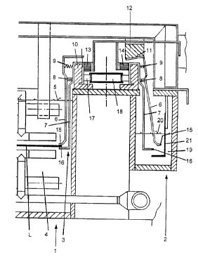
Fig. l shows a section through a portion of an electroplating plant for
printed circuit boards with
a plating section 1 and a stripping section 2. As far as the structure of the
plant does not refer to
the contact elements 15,16 in accordance with the invention, said structure is
basically known.
The printed circuit boards L are guided in one conveying plane through the
plating section 1 by
means of appropriate guide members (not shown). They are horizontally oriented
in the process
and are conveyed in horizontal direction (normal to the plane of the Figures).
The guide
members usually employed are rolls.
To advance the printed circuit boards L, the contact organs 3, which also
serve for making
electrical contact with the printed circuit boards L, are employed, said
contact organs being
designed as clamps in this case. Such clamps 3 may also be provided on the
opposite edge of the
printed circuit boards L, so that the plates may be grasped and advanced on
both sides (exterior
to the partial view in the Figure).
The clamps 3 are made of titanium, thus being resistant to the etching liquid
for treatment 4.
The printed circuit boards L are carried in the electroplating solution 4
(liquid level 5) in such
a manner that they are completely surrounded by liquid. Usually, printed
circuit boards are
treated that are provided with a base layer of copper on both sides so that
the current has to be
supplied to both sides. The stripping section 2 includes a stripping solution
19 suitable for
CA 02341218 2001-02-19
12
stripping the clamps 3 with the upper liquid level 20 as well as a counter
electrode 21.
The contacting clamps 3 are driven by an endless chain or by an endless cog
belt 17, made from
synthetic material for example, and are closely spaced in rows one behind the
other, the
intervals between them amounting to 6 cm for example. The cog belt is guided
by way of rolls
18. The clamps 3 are guided on a guide rail 10 by way of an internal clamp bar
7 which
encompasses said rail. The clamps 3 are thus passed through the plating
section 1 first, and then
through the stripping section 2.
The clamps 3 consist of two clamp bars 6, 7, which are joined together at the
pivot 8 so that the
external bar 6 may be pivoted toward the internal bar 7 against a force
provided by the pressure
spring 9. The pressure spring 9 is supported between the two bars 6 and 7
above the pivot 8. In
its idle position, the pressure spring 9 pushes the bars 6, 7 against each
other, so that the clamp
3 is closed. This is the case when the clamp 3 is guided in the plating
section 1. When the clamp
3 exits the plating section 1, the external bar 6 comes into contact with the
stop face 11 of a stop
rail 12, which compels the clamp to open against the force of the spring. The
clamp 3 being
opened, the printed circuit board L is released and can exit the plant. On
returning, the bar 6
continues to be in contact with the stop face 11 so that the clamp 3 remains
open.
Sliding contacts 13,14 feed the electric current to the clamps 3. To this
purpose, the internal bar
7 slides along the sliding contacts 13, 14. In the plating section 1 cathodic
polarity is imposed
upon the contact 13 whereas anodic polarity is imposed upon the sliding
contact 14 in the
stripping section 2.
Upon entering the plating section 1, the clamps 3 grasp the printed circuit
boards L, which are
entering said section as well, in the area of the galvanoedge. The spring 9
applies a force of
to 30 N onto the contact elements 15, 16 so that a very strong mechanical bond
is achieved
between the clamp 3 and the printed circuit board L. When the clamps 3 exit
the stripping
section Z, the external bar 6 runs off the stop face 11, thus allowing the
clamp 3 to close. The
end of the stop rail 12 with its stop face 11 is positioned in such a way that
the closing clamp
3 is capable of grasping a printed circuit board L entering the plant at this
place. Depending
CA 02341218 2001-02-19
13
upon the size of the printed circuit boards L and the spacing between the
clamps 3, four to
eight clamps may grasp one printed circuit board at the same instant of time.
While the printed circuit boards L are grasped by the clamps 3, catholic
polarity is imposed
upon the boards which are fed with electric current by the sliding contacts 13
and the clamps
3. After the opened clamps 3 have exited the plating section 1, they enter the
stripping section
2. There, the contact 14 and the clamps 3 impose anodic polarity upon them and
supply them
with electric current. Thanks to anodic polarity, metal that deposited on the
clamps 3 during
the electroplating process in the plating section 1 can be stripped off in the
stripping section
2.
Upper contact elements 15 and lower contact elements 16 in accordance with the
invention
are disposed at the tips of the contact bars 6, 7 for transmitting large
currents. Said contact
elements 15, 16 are strongly printed on corresponding locations on the surface
of the printed
circuit board L.
A first embodiment of a contact element 15 according to the invention is shown
in Fig. 2. The
contact element 15 is fastened to the stem 22 of the external clamp bar 6. The
contact element
16 (not here presented) is fastened to the stem 23 of the internal clamp bar 7
in like manner.
The contact elements 15,16 substantially consist of a contact foot 27 and of
the humps 24
fastened there onto with intervals 25 provided in between. Four humps 24 are
provided in this
embodiment, said humps being arranged on the corners of a square. On one side
the contact
humps 24 are provided with contact areas 26 which are delimited by the
boundary line 34. On
closing the clamp 3, the contact areas 26 are printed very strongly on
corresponding
contacting areas on the surfaces of the printed circuit boards. The planarity
of the contact
areas 26 permits to achieve an intimate electrical contact with very little
contact resistance
between the contact areas of the humps 24 and the surfaces of the printed
circuit boards. The
humps 24 are made from copper for making good electrical contact. In order to
achieve
sufficient corrosion resistance for the humps 24 to the liquid for treatment,
their copper top
surface is plated with a thick enough layer of gold. Alternatively, other
noble metals or
electrically conductive mixed oxides may be employed as a protective coating.
CA 02341218 2001-02-19
14
By providing intervals 25 between the humps 24, the liquid for treatment can
wash said
humps 24 even when the contacts 15,16 finely rest on the printed circuit
boards L. As a
result thereof probably, efficient cooling of the contacts 15,16 is achieved
so that the surfaces
of the printed circuit boards are not damaged through overheating.
A second embodiment of the contacts is illustrated in Fig. 3. In this case
too, the contact
elements 15 (16 not shown) consist of the contact foot 27 and of the humps 24
arranged on
said contact foot 27. In this case, the humps 24 are produced out of a
circular surface in which
grooves 25 are cut, which form the intervals between the humps 24. In this
case there are two
right-angled grooves 25 which subdivide the originally circular surface into
four
symmetrically arranged humps 24, each having the shape of a segment of a
circle. In this case
as well the various humps 24 are provided on one side with contact areas 26
which are
delimited by the boundary line 34.
Fig. 4 indicates a third embodiment for the contacts. In this case, the
contact foot 27 of the
contact elements 15 (16 not shown) has an elongate shape. The various humps 24
are
arranged in a row-shaped matrix and are produced by cuttings that
simultaneously form the
intervals (grooves) 25. The humps 24 are again provided on one side with plane
contact areas
26 which are delimited by the boundary line 34.
The elongate shape of the hump arrangement allows a large supporting surface
to be formed
on a very narrow galvanoedge, a large enough contact surface F being available
at the same
time. As a result, the width of the useless galvanoedge may be further reduced
Fig. 5 shows further embodiments for geometrical shapes of contact surfaces
26. Each contact
surface 26 is delimited by one boundary line 34. Stars, trifoliate or dumbbell-
shaped shapes
may be utilized. Furthermore, contact elements 26 may be used which have one
or several
serrated circles serving as contact areas 26.
Fig. 6 illustrates an alternative embodiment of a contacting clamp 3, the
inventive contact
elements 15, 16 being fastened to both bars 6, 7 of said clamp. In this case,
two paralleled
CA 02341218 2001-02-19
bars 6, 7 are provided The external bar 6 is connected to the internal bar 7
in such a way that
both are relatively slidable parallel to their longitudinal axis. The upper
end of the internal bar
7 is designed in such a way that it may be guided on a guide rail, in a
fashion as shown in Fig.
1 for example (guide rail 10). In this case, the stem 22 of the external bar 6
is guided in the
sliding bearings fastened to the stem 23 of the internal bar 7 in sliding
bearing bodies 28, 29
through a long hole 33 so that it is movable parallel to the longitudinal axis
of the stem. The
lower ends of the two bars are inclined at an angle of about 90° at
different heights but in the
same direction. The contact elements 15,16 are arranged at the ends of the
bent arms 30, 31.
The pressure spring 32 pushes the two arms 30, 31 against each other. The
spring 32 is
supported by the stationary internal bar 7 via the upper sliding bearing body
28 and by a
projection (not shown) fastened to the external bar 6.
The parallel motion of the external bar 6 relative to the internal bar 7
allows the contact areas
26 of the contact elements 15 and 16 to meet in a perfectly parallel
arrangement so that an
optimal contact of the contact areas 26 to the surfaces of the printed circuit
board L may be
achieved, said printed circuit board being oriented in such a way as to also
be parallel to the
contact areas 26.
CA 02341218 2001-02-19
16
LISTING OF REFERENCE NUMERALS
1 plating section
2 stripping section
3 contacting clamp
4 liquid for treatment
liquid level of the liquid for treatment 4
6 external clamp bar
7 internal clamp bar
8 pivot
9 pressure spring
guide rail
11 stop face
12 stop rail
13 sliding contact
14 sliding contact
upper contact element
16 lower contact element
17 cog belt
18 rolls
19 stripping solution
liquid level of the stripping solution
21 counter electrode
22 stem of the external bar 6 of the contacting clamp 3
23 stem of the internal bar 7 of the contacting clamp 3
24 hump
intervals between the humps 24
26 contact area on the hump 24
27 contact foot
28 sliding bearing body
29 sliding bearing body
CA 02341218 2001-02-19
17
30 bent arm of the external bar 6 of the contacting clamp 3
31 bent arm of the internal bar 7 of the contacting clamp 3
32 pressure spring
33 long hole
34 boundary line
L printed circuit board