Note: Descriptions are shown in the official language in which they were submitted.
CA 02341439 2001-02-21
WO 00/13388 PCT/tIS99/17599
-1-
A CONSTRAINED-ENVELOPE DIGITAL-COMMUNICATIONS
TRANSMISSION SYSTEM AND METHOD THEREFOR
TECHNICAL FIELD
The present invention relates generally to the field of digital
communications.
More specifically, the present invention relates to the field of constrained-
envelope
digital transmitter circuits.
BACKGROUND ART
A wireless digital communications system should ideally refrain from using any
portion of the frequency spectrum beyond that actually required for
communications.
Such a maximally efficient use of the frequency spectrum would allow the
greatest
number of communications channels per given spectrum. In the real-world,
however,
some spectral regrowth (i.e., increase in spectral bandwidth) is inevitable
due to
1 S imperfect signal amplification.
In wireless communication systems various methodologies have been used to
minimize spectral regrowth. Some conventional methodologies utilize complex
digital
signal processing algorithms to alter a digitally modulated transmission
signal in some
manner conducive to minimal spectral regrowth. Such complex algorithmic
methodologies are well suited to low-throughput applications, i.e., those less
than 0.1
Mbps (megabits per second), such as transmission of vocoder or other audio
data. This
is because the low throughput rate allows sufficient time between symbols for
the
processor to perform extensive and often repetitive calculations to effect the
required
signal modification. Unfortunately, high-throughput applications, i.e., those
greater than
0.1 Mbps, such as the transmission of high-speed video data, cannot use
complex
processing algorithms because the processing power required to process the
higher data
rate is impractical.
A digital signal processing methodology may be used with the transmission of
burst signals. With burst transmissions, the interstitial time between bursts
may be used
to perform the necessary complex computations based upon an entire burst. This
methodology is not practical when continuous (as opposed to burst)
transmission is
used.
CA 02341439 2001-02-21
WO 00/13388 PCT/US99/17599
-2-
A conventional form of post-modulation pulse shaping to minimize spectral
bandwidth utilizes some form of Nyquist-type filtration, such as Nyquist, root-
Nyquist,
raised cosine-rolloff etc. Nyquist-type filters are desirable as they provide
a nearly ideal
spectrally constrained waveform and negligible inter-symbol interference. This
is
5 achieved by spreading the datum for a single constellation phase point over
many unit
baud intervals in such a manner that the energy from any given phase-point
datum does
not interfere with the energy from preceding and following phase-point data at
the
appropriate baud-interval sampling instants.
The use of Nyquist-type filtration in a transmission circuit produces a
filtered
signal stream containing a pulse waveform with a spectrally constrained
waveform. The
degree to which a Nyquist-type pulse waveform is constrained in bandwidth is a
function of the excess bandwidth factor, a. The smaller the value of a, the
more the
pulse waveform is constrained in spectral regrowth. It is therefore desirable
to have the
value of a as small as possible. However, as the value of a is decreased, the
ratio of the
spectrally constrained waveform magnitude to the spectrally unconstrained
waveform
magnitude is increased. The spectrally unconstrained waveform is the waveform
that
would result if no action were taken to reduce spectral regrowth. Typical
designs use a
values of 0.1 to 0.5. For an exemplary a value of 0.2, the magnitude of the
spectrally
constrained waveform is approximately 1.8 times that of the unconstrained
waveform.
20 This means that, for a normalized spectrally unconstrained waveform
magnitude power
of 1.0, the transmitter output amplifier must actually be able to provide an
output power
of 3.24 (1.82) to faithfully transmit the spectrally constrained waveform.
This poses
several problems.
When the transmitter output amplifier is biased so that the maximum spectrally
25 unconstrained waveform (1.0 normalized) is at or near the top of the
amplifier's linear
region, all "overpower" will be clipped as the amplifier saturates. Such
clipping causes
a marked increase in spectral regrowth, obviating the use of Nyquist-type
filtration.
When the transmitter output amplifier is biased so that the maximum spectrally
constrained waveform ( 1.8 normalized) is at or near the top of the
amplifier's linear
30 region, the spectrally unconstrained waveform is at only 56 percent (i.e.,
~~.8) of the
amplifiers peak linear power. This results in an inefficient use of the output
amplifier.
CA 02341439 2001-02-21
WO 00/13388 PCT/US99/17599
-3-
Also, the biasing of the transmitter output amplifier so that the spectrally
constrained waveform is at or near the top of the amplifier's linear region
requires that
the output amplifier be of significantly higher power than that required for
the
transmission of a spectrally unconstrained waveform. Such a higher-power
amplifier is
5 inherently more costly than its lower-power counterparts.
DISCLOSURE OF INVENTION
It is an advantage of the present invention that a circuitry and a methodology
are
provided that allow a transmitter output amplifier to be biased so that the
spectrally
10 unconstrained waveform is at or near the top of the amplifier's linear
region without
incurring clipping of a spectrally constrained waveform.
It is another advantage of the present invention that a circuitry and
methodology
are provided that allow a spectrally constrained waveform to have
approximately the
same magnitude as the spectrally unconstrained waveform without effecting a
15 significant increase in spectral regrowth.
It is another advantage of the present invention that a circuitry and
methodology
are provided which allow a spectrally constrained waveform to be utilized with
a
continuous transmission scheme.
It is another advantage of the present invention that a circuitry and
methodology
20 are provided which allow efficient use of a transmitter output amplifier,
thus allowing
higher power output for a given output amplifier and a given bandwidth
constraint than
was previously feasible.
It is another advantage of the present invention that a circuitry and
methodology
are provided which allow efficient use of a transmitter output amplifier,
which allows a
25 lower-power amplifier to be used for achieving given bandwidth constraints,
thus
effecting a significant saving in the cost thereof.
These and other advantages are realized in one exemplary form by a constrained-
envelope digital communications transmitter circuit. The circuit includes a
phase
mapper configured to generate a phase point for each of successive unit baud
intervals.
30 A first pulse-spreading filter is coupled to the phase mapper and
configured to generate
a filtered signal stream in which energy from each phase point is spread over
a plurality
of unit baud intervals. A second pulse-spreading filter has an input
responsive to the
CA 02341439 2001-02-21
WO 00/13388 PCT/US99/17599
-4-
filtered signal stream and is configured to generate a constrained-bandwidth
error signal
stream. A combining circuit is configured to combine the filtered signal
stream and the
constrained-bandwidth error signal stream.
BRIEF DESCRIPTION OF DRAWINGS
A more complete understanding of the present invention may be derived by
referring to the detailed description and claims when considered in connection
with the
Figures, wherein like reference numbers refer to similar items throughout the
Figures,
and:
FIG. 1 depicts a simplified block diagram of a digital communications system
in
accordance with a preferred embodiment of the present invention;
FIG. 2 depicts a block diagram of a constrained-envelope digital
communications
transmitter circuit in accordance with a preferred embodiment of the present
invention;
FIG. 3 depicts a 16-P-APSK constellation illustrating a locus of a quadrature
1 S phase-point signal stream over twelve exemplary consecutively mapped phase
points in
accordance with a preferred embodiment of the present invention;
FIG. 4 depicts a plurality of signal streams in accordance with a preferred
embodiment of the present invention;
FIG. 5 depicts the phase-point constellation of FIG. 3 illustrating an
exemplary
locus of a filtered signal stream over the twelve consecutively mapped phase
points of
FIG. 3 in accordance with a preferred embodiment of the present invention;
FIG. 6 depicts a pair of Nyquist-type data bursts in accordance with a
preferred
embodiment of the present invention; and
FIG. 7 depicts a noise-influenced constellation illustrating constrained-
envelope
phase-point probabilities of the phase points of the constellation of FIG. 3
in accordance
with a preferred embodiment of the present invention.
BEST MODE FOR CARRYING OUT THE INVENTION
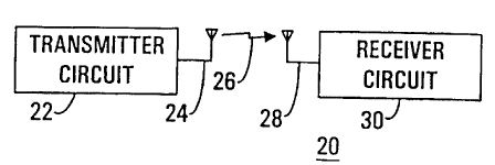
FIG. 1 depicts a simplified block diagram of a digital communications system
20 and
FIG. 2 depicts a block diagram of a constrained-envelope digital
communications
transmitter circuit 22 in accordance with a preferred embodiment of the
present
invention. The following discussion refers to FIGs. 1 and 2.
1826-31 OPC'f ~ 02341439 2001-02-21 ~~ r~ ~ ' v
~~~ a 0 ~a P R ~ 2000
-5_
Digital communications system 20, as depicted ili FIG. l, includes a
transmitter
circuit 22 and a transmitter antenna 24 together configured to modulate and
transmit a
radio-frequency (RF) broadcast signal 26 to a receiver antenna 28 and a
receiver circuit
30, together configured to receive and demodulate RF broadcast sigrtai 26.
Those
skilled in the art will appreciate that the embodiment of system 20 depicted
is a
simplistic one for purposes of discussion only. In normal use, system 20 would
likely
be a complex system eonsistin$ of many more components and broadcast signals.
it
will be appreciated that the use of such a complex conununications system for
system
20 in no way departs from the spirit of the present invention or the scope of
the
appended claims. Moreover, nothing requires signal 261o be an RF signal
because the
teaching of the present invention may also be applied to cable and wireline
di~rital
communications.
Transmitter circuit 22 has a binary data source 32 providing a binary input
signal
stream 34. Binary data source 32 may be any circuitry, device, or combination
thereof
IS producing.input sig~l stream 34. Input signal stream 34 is made up of
binary data that
may be pre-encoded in any desired manner. That is, input signal stream 34 may
be
made up of data that has no encoding, concatenated encoding, Reed-Solomon
block
encoding, or any other form of encoding desired for or required of the
communications
scheme in use.
In the preferred embodiment, input signal stream 34 is a stream of continuous
data
(as contrasted with burst data) passing to an input of a convolutional encoder
36.
Convolutional encoder 36 convolutionally encodes (c.g., Viterbi encodes) input
signal
stream 34 into an encoded signal stream 38. The use of convolutional encoder
36 in
transmitter circuit 22 and a like convolutional decoder (not shown) in
receiver circuit 30
significantly reduces the error rate of the overall signal in a manner well
understood by
those skilled in the art. However, encoder 36 may apply turbo encoding or
other types
of encoding in some alternate embodiments, and convoiutionat encoder 36 may be
omitted altogether in other alternate embodiments.
Interleaves 4U temporally decorrelates encoded signal stream 3A to produce an
interleaved signal stream 42. That is, the symbols making up the binary signal
stream
are temporally decorrelated (i.e., separated) in transmitter circuit 22 and
temporally
correlated in receiver circuit 3U. This is done so that correlated errors
produced by
t~~.~v~'T'. ~'vl ~l~L- ~
~L~ . .. ., ~ ....
CA 02341439 2001-02-21
WO 00/I3388 PCT/US99/17599
-6-
downstream transmitter components, discussed hereinbelow, will then be
decorrelated
through a complimentary de-interleaver located in receiver circuit 30 before
convolutional decoding in receiver circuit 30.
In the preferred embodiment, interleaved signal stream 42 passes to an input
of a
phase mapper 44. Those skilled in the art will appreciate that interleaver 40
is not
desired in all embodiments of transmitter circuit 22, for example when
convolutional
encoder 36 is omitted. When interleaver 40 is omitted, encoded signal stream
38 is
passed directly to the input of phase mapper 44. When both convolutional
encoder 36
and interleaver 40 are omitted, binary input signal stream passes directly to
the input of
I 0 phase mapper 44.
FIG. 3 depicts a sixteen phase-point polar amplitude and phase shift keying
(16-P
APSK) constellation 46 illustrating a locus 48 of a quadrature phase-point
signal stream
50 (FIG. 2) over twelve exemplary sequential phase points 52 in accordance
with a
preferred embodiment of the present invention. The following discussion refers
to
15 FIGS. 2 through 3.
Phase mapper 44 maps symbols (i.e., binary data units) present in interleaved
signal stream 42, encoded signal stream 38, or input signal stream 34, into
phase points
54 in phase-point constellation 46. While constellation 46 is depicted in FIG.
3 as a 16-
P-APSK constellation, those skilled in the art will appreciate that the
circuitry and
20 methodology of the present invention may be applied to all forms of
constellations. The
present invention is especially beneficial when used with constellations
having phase
point rings of different magnitudes, i.e., amplitude and phase-shift keying
(APSK)
constellations. This is true because APSK constellations, requiring amplitude
modulation of the signal, desirably use linear amplifiers to reproduce that
amplitude
25 modulation.
Each phase point 54 in constellation 46 represents a plurality, in this
example four,
of symbols. The values of the symbols in a given phase point 54 determine the
location
of that phase point 54 within constellation 46 in a manner well known to those
skilled in
the art.
30 Each quadrature phase point 54 may be thought of as having a vector value
expressed as I,Q in the Cartesian coordinate system, where I is the in-phase
(abscissa)
value and Q is the quadrature (ordinate) value of the vector, or expressed as
M,~ in the
CA 02341439 2001-02-21
WO 00/13388 PCT/US99/17599
_'7_
polar coordinate system, where M is the magnitude and ~ is the phase angle of
the
vector. In this discussion, the M,~ designation will be used throughout, as
the vector
magnitude is the most discussed vector component.
In the exemplary 16-P-APSK constellation 46 of FIG. 3, each phase point 54
S resides upon an outer ring 56 or an inner ring 58. Phase-points 54 residing
upon outer
ring 56 are outer-ring or maximum-magnitude phase points 60. That is, outer-
ring
phase points 60 have a maximum magnitude (maximum value of M) as represented
by
the radius of outer ring 56. For purposes of discussion, the magnitudes of
outer-ring
phase points 60 are normalized to 1.00.
10 Irmer-ring phase points 62, i.e., those phase points 54 residing upon inner
ring 58,
have a lesser magnitude as represented by the radius of inner ring 58. For the
exemplary
16-P-APSK constellation 46 depicted in FIG. 3, the magnitudes of inner-ring
phase
points 62 may desirably be approximately 0.63 when outer-ring phase point 60
magnitudes are normalized to 1.00.
15 FIG. 4 depicts a plurality of signal streams, in accordance with a
preferred
embodiment of the present invention. The following discussion refers to FIGs.
2
through 4.
The output of phase mapper 44 is phase-point signal stream 50. Phase mapper 44
processes one phase point 54 per unit baud interval 64. That is, phase-point
signal
20 stream 50 consists of a series of consecutive phase-point pulses 66, each
of which
represents one phase point 54, whose leading edges are one unit baud interval
64 apart.
Those skilled in the art will appreciate that other embodiments of phase-point
signal
stream 50 are equally valid, that the embodiment utilized is dependent upon
the circuitry
producing and processing phase-point signal stream 50, and that the use of
other
25 embodiments of this or any other signal stream does not depart from the
spirit of the
present invent nor the scope of the appended claims.
FIGs. 3 and 4 illustrate a series of twelve exemplary sequential phase points
52,
representative of a random data stream processed by transmitter circuit 22
(FIG.2).
These twelve exemplary phase points 52 reside at temporally consecutive
locations
30 labeled to, tl, t2, t3, t4, ts, tb, t~, tg, t9, t,o, and tl,. These labels
represent sequential
integral times at unit baud intervals 64, i.e., integral-baud times, and
indicate the
CA 02341439 2001-02-21
WO 00/13388 PCTNS99/17599
-g_
leading-edge times of phase-point pulses 66. For purposes of simplification
within this
discussion, any occurrence at time tN shall be referred to as "occurrence tN".
For
example, an exemplary phase point 52 occurring at time t2 shall be referred to
as phase
point t2, and the associated phase-point pulse 66 whose leading edge occurs at
time t2
S shall be referred to as phase-point-signal pulse tz. In other words, at time
t2, phase point
t2 is clocked and phase-point-signal pulse tz begins. One unit baud interval
64 later, at
time t3, phase point t3 is clocked and phase-point pulse t3 begins. This
process continues
indefinitely, with twelve exemplary phase points to through t" depicted in
FIG. 3 and
twelve corresponding phase-point-signal pulses to through t, l depicted in
phase-point
signal stream 50 of FIG. 4.
Phase point to is an outer-ring phase point 60. Phase-point-signal pulse to
therefore has an outer-ring magnitude 68. In like manner, phase point t, is an
inner-ring
phase point 62 and phase-point-signal pulse t, has an inner-ring magnitude 70.
Table 1
below illustrates the magnitudes for phase-point-signal pulses to through t~,.
Phase-Point-Signal Magnitude
Pulse
to Outer-Rin 68
t, Inner-Rin 70
tZ Outer-Ring 68
t3 Outer-Rin 68
t4 Inner-Rin 70
is Outer-Rin 68
tb Outer-Rin 68
t7 Outer-Rin 68
t8 Outer-Rin 68
t9 Inner-Rin 70
tea Outer-Rin 68
t" Inner-Ring 70
Table 1 -- Phase-Point Pulse Magnitudes
Phase-point signal stream 50 effects locus 48 through constellation 46. Locus
48
coincides with the location of each exemplary phase point to through t~, in
turn at unit
baud intervals 64. In FIG. 3, locus 48 is depicted as effecting a minimum
distance
(straight line) path between adjacent exemplary phase points 52. Those skilled
in the art
CA 02341439 2001-02-21
WO 00/13388 PCT/US99/17599
-9-
will appreciate that locus 48 is so depicted solely for the sake of
simplicity, and that in
actual practice, locus 48 instantly jumps or snaps between exemplary phase
points 52 in
a discontinuous manner.
FIG. 5 depicts an expanded phase-point constellation 46' illustrating a locus
72 of
a filtered signal stream 74 (FIG. 2) over twelve exemplary sequential phase
points 52 in
accordance with a preferred embodiment of the present invention. The following
discussion refers to FIGs. 2 through 5.
In the preferred embodiment, phase-point signal stream 50 passes to the input
of a
pulse-spreading filter 76, preferably realized as a Nyquist-type filter, such
as a Nyquist,
root-Nyquist, raised cosine-rolloff, etc., filter. Pulse-spreading filter 76
filters phase-
point signal stream 50 into filtered signal stream 74, depicted in FIG. S. In
orthogonal
frequency division multiplex (OFDM) systems, also known as multitone
modulation
(MTM) systems, pulse-spreading filter 76 may be implemented using a
transmultiplexer
or equivalent circuitry.
In accordance with Shannon's theory, well known to those skilled in the art,
pulse-
spreading filter 76 produces at least two (only two in the preferred
embodiment) output
filtered-signal pulses 78, i.e., complex samples of filtered signal stream 74,
for each
input phase-point pulse 66 received. This is demonstrated in FIG. 4 where
filtered
signal stream 74 possesses two filtered-signal pulses 78 per unit baud
interval 64. In the
preferred embodiment, filtered-signal pulses 78 consist of alternating on-time
pulses 80,
i.e., samples of filtered signal stream at integral unit baud intervals 64,
and off time
pulses 82, i.e., samples of filtered signal stream 74 between integral unit
baud intervals.
In effect, filtered signal stream 74 is made up of two interleaved data
streams, an on-
time signal stream 84 and an off time signal stream 86.
On-time signal stream 84 is substantially a version of phase-point signal
stream
S0, wherein each phase-point pulse 66 may have been reduced in duration from
one unit
baud interval 64 to a half unit baud interval 88 to become on-time pulse 80
while
maintaining substantially the same relative leading-edge time. That is,
filtered-signal
pulse to has substantially the same magnitude and substantially the same
leading edge
time as phase-point pulse to with approximately one-half the duration.
However, with
Nyquist-type filters that do not implement a pure Nyquist filter, on-time
signal stream
84 will not be precisely a version of phase-point signal stream S0. Of course,
those
CA 02341439 2001-02-21
WO 00/13388 PCT/US99/17599
-10-
skilled in the art will appreciate that signal streams 74 and 84 may be
delayed from
signal stream 50 by a delay imposed by filter 76, and that signal streams 84
and 86 may
be kept as separate parallel streams in which each pulse exhibits
substantially the
duration of phase-point pulses 66.
The generation of both on-time pulses 80 and off time pulses 82 by pulse-
spreading filter 76 effectively populates expanded constellation 46' (FIG. 5)
with on
time phase-points 90 (circles) and off time phase points 92 (squares). The
original
phase points 54 of constellation 46 (FIG. 3), i.e., the phase points carrying
the
intelligence to be communicated by transmitter circuit 22, are on-time phase
points 90
10 of expanded constellation 46'.
Added to expanded constellation 46' are off time phase points 92, with each
off
time phase-point 92 occurring or otherwise carrying the intelligence to define
the signal
approximately midway in time between consecutive on-time phase points 90.
Therefore, exemplary sequential phase points 52 become exemplary filtered
phase
points 94. Exemplary filtered phase points 94 are made up of alternating
exemplary on-
time filtered phase points 96 and exemplary off time filtered phase points 98,
and reside
at or otherwise convey the intelligence to define the signal at temporally
consecutive
locations labeled tp, t0.s~ tl~ tl,s~ t2~ t2.s~ t3~ t3.>> t4~ t4.s~ ts~ ts.s,
tb~ tb.s~ t7~ t7.s~ t8~ t8.s~ t9~ t9.5~
tio, t,o.s, and t, i. In FIG. 5, exemplary on-time filtered phase points 96
are located at
20 integral-baud times (to, tl, t2, etc.), whereas exemplary off time filtered
phase points 98
are located at fractional-baud (non-integral-baud) times (to.s, ti.s, tz.s~
etc.).
The generation of off time phase points 92 approximately midway in time
between consecutive on-time phase points 90 causes filtered signal locus 72 to
effect
excursions having local peak magnitudes 99 greater than outer-ring magnitude
68. Such
25 excursions occur because the immediate position of locus 72 at any given
instant in time
is not only a result of those phase points 54 proximate that position, but of
a plurality of
phase points 54 both preceding and following that instant in time. That is, in
the
preferred embodiment, the determination of the position of locus 72 at time
t2.s (i.e.,
coincident with off time phase point t2,s) is determined not only by the
positions of
30 phase points t2 and t3, but by the positions of numerous phase points 54
preceding phase
point t2.s (i.e., phase points t2, t,.s, t,, to_s, etc.) and the positions of
numerous phase
points 54 following phase point t2.s (i.e., phase points t3, t3,s, t4, t4,;,
etc.).
CA 02341439 2001-02-21
WO 00/13388 PCT/US99/17599
-11-
This phenomenon is illustrated in FIG. 6, which depicts a pair of Nyquist-type
datum bursts 100 in accordance with a preferred embodiment of the present
invention.
The following discussion refers to FIGs. 2, 4, 5, and 6.
In the preferred embodiment, pulse-spreading filter 76 is realized as a
Nyquist-
type filter. Therefore, when a single phase-point pulse 66 is filtered by
pulse-spreading
filter 76, that single pulse 66 is transformed into a Nyquist-type datum burst
100
extending over a plurality of unit baud intervals 64. It is a property of
Nyquist-type
filters that datum burst 100 attains a datum-burst peak value 102 (i.e., a
local peak
magnitude) at the primary sampling time of the specific phase-point pulse 66
(i.e., at
time t2 for phase-point pulse t2), and attains a zero datum-burst value 104
(i.e., is equal
to zero) at integral unit baud intervals 64 preceding and following peak datum-
burst
value 102 (i.e., at times ..., t_,, to, ti, and t3, t4, ts, ..., for phase
point pulse t2). In this
manner, the energy of each pulse 78 is spread over a plurality of baud
intervals 64
preceding and following the clocking instant (time t2).
1 S FIG. 6 illustrates Nyquist-type datum bursts 100 for phase-point pulses tz
and t3,
with datum burst t2 depicted as a solid line and datum burst t3 depicted as a
dashed line.
As an example, it may be seen from FIG. 6 that at time t2 the value of datum
burst t2 is
peak datum-burst value 102. At every other time separated from time tz by an
integral
number of unit baud intervals 64, the value of datum burst t2 is zero. An
analogous
condition occurs for datum burst t3.
The value of locus 72 is, at each moment in time, the sum of all datum bursts
100
at that moment. In the simplified two-datum-burst example of FIG. 6, locus 72,
depicted by a dotted line, is the sum of datum burst t2 and datum burst t3.
Since datum
bursts t2 and t3 are zero at each integral time tN except times t2 and t3, the
value of locus
72 is also zero except at times t2 and t3, where it assumes the peak values of
datum
bursts t2 and t3, respectively.
The value of locus 72 at any instant in time between integral-baud times is
the
sum of the values of all datum bursts 100 at that instant. For example, in
FIG. 6 where
only two datum bursts 100 are considered, locus 72 has a value at time tz.s
that is the
sum of the values of datum bursts t2 and t3 at time tz.s. Since datum bursts
tz and t3 both
have significant positive values at time t2.5, locus 72 has a value
significantly greater
than the maximum values of either datum burst t2 or datum burst t3.
CA 02341439 2001-02-21
WO 00/13388 PCTNS99/17599
-12-
Since locus 72 describes the sum of all datum bursts 100, locus 72 is a
function of
the shape of the curves (FIG.6) describing those datum bursts 100. That is,
locus 72 is a
function of a filtered-signal peak magnitude component of a filtered-signal
complex
digital value at any given point. The shape of the datum-burst curve is a
function of the
excess bandwidth factor, a, a design property of pulse-spreading filter 76.
The smaller
the value of a, the more locus 72 may rise above the peak datum burst values
102 of
adjacent datum bursts 100. Typical designs of pulse-spreading filters 76 use a
values of
0.1 to 0.5. For like-valued adjacent phase points 54 and an a value of 0.2, a
maximum
excursion magnitude 105 (i.e., the potential local peak magnitude 99 of locus
72) is
approximately 1.8 times the value of the maximum phase-point magnitude. That
is, the
magnitude of the constrained envelope is approximately 1.8 times that of the
unconstrained envelope. In the preferred embodiment depicted in FIGs. 3, 4,
and 6, on-
time phase points t2 and t3 are both outer-ring phase points 60 having a
normalized
outer-ring magnitude 68 of 1.00. Therefore, off time phase point t2,5 may have
a
normalized maximum excursion magnitude 105 of 1.8. This implies that
transmitter
circuit 22, to faithfully transmit phase point t2.5 without excessive
distortion, and
without the benefit of the present invention, would require an output power of
3.24
( 1.82) times the power required to transmit phase point t2 or t3, which are
representative
of the highest magnitude intelligence-carrying phase points 54. This
represents an
inefficient use of available power.
The following discussion refers to FIGS. 2, 4, and 5.
Off time signal stream 86, a portion of filtered signal stream 74, passes from
an
output of pulse-spreading filter 76 to an input of an off time constrained-
envelope
generator 106. It is the task of off time constrained-envelope generator 106
to produce
an off time constrained-bandwidth error signal stream 108 from off time signal
stream
86. A complex summing or combining circuit 110 combines off time constrained-
bandwidth error signal stream 108 with a delayed version of filtered signal
stream 74
(discussed below) to produce a constrained-envelope signal stream 112.
Constrained-
envelope signal stream 112 is effectively filtered signal stream 74 with
compensation
for excursions of locus 72 with magnitudes greater than a predetermined
magnitude,
such as outer-ring magnitude 68.
CA 02341439 2001-02-21
WO 00/13388 PCT/US99/17599
-13-
A quadrature threshold generator 118 generates a quadrature threshold signal
120.
In the preferred embodiment, threshold signal 120 is a steady-state, constant
signal
having a value approximately equal to outer-ring magnitude 68. Threshold
signal 120 is
used to establish a reference with which off time signal stream 86 is
compared. Those
skilled in the art will appreciate that threshold signal 120 may assume many
forms and
values in keeping with the methodology and circuitry incorporated in the
comparison.
The use of other forms and/or other values does not depart from the spirit of
the present
invention nor from the scope of the appended claims.
Threshold signal 120 and off time signal stream 86 are combined in an off time
complex summing or combining circuit 122 to produce an off time difference
signal
stream 124. Off time difference signal stream 124 is made up of a series of
off time
difference pulses 126 whose values are the difference between the values of
equivalent
off time pulses 82 and the value of threshold signal 120. Since any given off
time pulse
82 may have a value greater than, equal to, or less than the value of
threshold signal 120,
I S off time difference signal stream 124 would normally be made up of a
combination of
off time difference pulses 126 having positive, zero, and negative values.
Off time difference signal stream 124 is passed to the input of an off time
discriminator 128 to produce an off time error signal stream 130. In the
preferred
embodiment, off time error signal stream 130 is a variation of off time
difference signal
stream 124 in which all off time difference pulses 126 having positive values
are passed
unchanged as off time error pulses I 32 while all other off time difference
pulses 126 are
passed as zero-value pulses (i.e., eliminated). In other words, off time error
signal
stream 130 is formed from pulses, the timing of which coincide with excursions
of locus
72 beyond threshold signal 120 and the magnitudes of which correspond to the
degree to
which locus 72 passes beyond threshold signal 120.
Off time error signal stream 130 is then passed to or otherwise drives the
input of
an off time pulse-spreading filter 134. Off time pulse-spreading filter 134 is
substantially identical to first pulse-spreading filter 76 in the preferred
embodiment.
That is, in the preferred embodiment, both pulse spreading filters 76 and 134
are
realized as Nyquist-type filters with substantially identical transfer
characteristics. Off
time pulse-spreading filter 134 produces off time constrained-bandwidth error
signal
stream 108 and completes the action of off time constrained-envelope generator
106.
CA 02341439 2001-02-21
WO 00/13388 PCT/US99/17599
-14-
Within off time constrained-envelope generator 106, off time pulse-spreading
filter 134 receives one off time error pulse 132 from off time discriminator
128 per
selected unit baud intervals 64. Off time pulse-spreading filter 134 then
transforms
each off time error pulse 132 into a Nyquist-type error burst extending over a
plurality
S of unit baud intervals. The error burst signal resulting from a single error
pulse 132 has
the shape of the data bursts shown in FIG. 6. Since off time pulse-spreading
filter 134
is a Nyquist-type filter, each error burst attains an error-burst peak value
at the primary
sampling time of the specific off time error pulse 132 (i.e., at time t2,; for
error pulse
t2,;), and attains a zero error-burst value at integral unit baud intervals 64
preceding and
following the peak error-burst value (i.e., at times ..., t_i.;, to.;, t,.;,
and t3,;, t4.;, ts.s~ ...,
for error pulse t2.;). In this manner, the energy of each off time constrained-
envelope
error pulse 136 is spread over a plurality of baud intervals 64 preceding and
following
the clocking instant (time t2,5). This results in the conversion of off time
error signal
stream 130 into off time constrained-bandwidth error signal stream 108. Off
time
constrained-bandwidth error signal stream 108 is made up of off time
constrained-
envelope error pulses 136. This operation is essentially the same as the
operation of
pulse-spreading filter 76 in the conversion of phase-point signal stream 50
into filtered
signal stream 74 described hereinabove.
Since off time constrained-envelope error pulses 136 are derived from off time
pulses 82, the error-burst peak and zero values occur approximately midway
between
integral baud times, i.e., at baud times to.;, t~,;, t2.;, etc., hence between
datum-burst peak
and zero values 102 and 104 of filtered signal stream 74.
The production of off time constrained-bandwidth error signal stream 108
completes the operation of off time constrained envelope generator 106.
Filtered signal stream 74 is also passed to the input of a delay element 138.
Delay
element 138 produces delayed signal stream 140, which is effectively filtered
signal
stream 74 delayed sufficiently to compensate for the propagation and other
delays
encountered in off time constrained-envelope generator 106, and particularly
in off time
pulse-spreading filter 134. In other words, delayed signal stream 140 is
filtered signal
stream 74 brought into synchronization with off time constrained-bandwidth
error signal
stream 108.
~:.,:~.
CA 02341439 2001-02-21
WO 00/13388 PCT/US99/17599
-15-
Combining circuit I 10 combines filtered signal stream 74, in the form of
delayed
signal stream 140, and off time constrained-bandwidth error signal stream 108
to reduce
peak magnitude components of filtered signal stream 74. A resultant
constrained-
envelope signal stream 112 is made up of a series of digital pulses 142 whose
values are
the difference between the values of corresponding filtered-signal pulses 78
and off time
constrained-envelope error pulses 136. The result is a series of digital
pulses 142 whose
values do not appreciably exceed outer-ring magnitude 68 of expanded
constellation 46'
in the preferred embodiment. In other embodiments, the envelope may be
constrained
to any desired magnitude.
In some embodiments of the present invention, certain of outer-ring phase
points
60 may have magnitudes greater than outer-ring magnitude 68, i.e., may be
located
beyond outer ring 56. This condition may occur as a result of pulse-spreading
filter 76
executing certain Nyquist-type functions, such as a root-Nyquist filter, well
known to
those skilled in the art. In such an embodiment, transmitter circuit 22
contains an on-
time constrained envelope generator 106' in addition to off time constrained-
envelope
generator 106 discussed above.
On-time signal stream 84, also a portion of filtered signal stream 74, passes
from
an output of pulse-spreading filter 76 to an input of on-time constrained-
envelope
generator 106'. It is the task of on-time constrained-envelope generator 106'
to produce
an on-time constrained-bandwidth error signal stream 108' from on-time signal
stream
84. Combining circuit I 10 combines both off time and on-time constrained-
bandwidth
error signal streams 108 and 108' with the delayed version of filtered signal
stream 74
(discussed below) to produce constrained-envelope signal stream 112.
On-time constrained-envelope generator 106' operates in a manner analogous
with
the operation of off time constrained-envelope generator 106. Threshold signal
120 and
on-time signal stream 84 are combined in an on-time complex summing or
combining
circuit 122' to produce an on-time difference signal stream 124'. On-time
difference
signal stream 124' is passed to the input of an on-time discriminator 128' to
produce an
on-time error signal stream 130'. On-time error signal stream 130' is then
passed to the
input of an on-time pulse-spreading filter 134', which produces on-time
constrained
bandwidth error signal stream 108'. Like off time pulse-spreading filter 134,
on-time
pulse-spreading filter 134', is substantially identical to first pulse-
spreading filter 76.
CA 02341439 2001-02-21
WO 00/13388 PCT/US99/17599
-16-
Since on-time constrained-envelope error pulses (not shown) are derived from
on-
time pulses 80, the error-burst peak and zero values occur at integral baud
times, i.e., at
baud times t,, t2, t3, etc., hence between datum-burst peak and zero values
102 and 104
of filtered signal stream 74.
Combining circuit 110 combines filtered signal stream 74, in the form of
delayed
signal stream 140, with both off time and on-time constrained-bandwidth error
signal
stream 108 and 108' to reduce peak magnitude components of filtered signal
stream 74.
Alternate embodiments may incorporate alternate techniques for generating one
or
more constrained bandwidth error signal streams for combining with filtered
signal
stream 74. For example, in one alternate embodiment, on-time constrained-
envelope
generator 106' may be omitted. In another embodiment, off time constrained
envelope
generator 106 may time error pulses 132 to occur at on-time instants. In
another
embodiment, a constrained-envelope generator 106 may monitor both on-time
signal
stream 84 and off time signal stream 86, predict when during a baud interval
64 a local
peak magnitude 99 occurs, generate two successive error pulses 132 whose
relative
magnitudes are proportional to the predicted local peak magnitude instant and
are timed
to produce a error burst peaks and zeros synchronized to on-time signal stream
84. In
this alternate embodiment, as an example, if filtered signal locus 72 is found
to exceed
threshold signal 120 by an amount "X", with a peak predicted to occur at 25%
of the
duration between a first on-time filtered phase point 96 and a second on-time
filtered
phase point 96 (i.e., SO% of the duration between an on-time filtered phase
point 96 and
a subsequent off time filtered phase point 98, then an error pulse 132 of
magnitude
0.75X may be timed to occur at a first on-time instant and an error pulse 132
of
magnitude 0.25X may be timed to occur at a subsequent on-time instant. In yet
another
embodiment, an interpolator may be used to generate a greater number of
filtered signal
stream samples per baud, and this greater number of samples per baud monitored
to
more precisely predict the instant of local peak magnitude 99. These and other
equivalent alternative embodiments are included within the scope of the
present
invention.
A side effect of this methodology is that locus 72 at integral unit baud
intervals 64
adds a signal-dependent, baud-limited noise factor to the positions of phase
points 54 in
constellation 46 (FIG. 3). This results in transmitter circuit 22 transmitting
a "noise-
, CA 02341439 2001-02-21
WO 00/13388 PCT/US99/17599
-17-
influenced" phase-point constellation 46". In FIG. 7, noise-influenced
constellation 46"
is depicted illustrating constrained-envelope phase-point probabilities 144 of
phase
points 54 in accordance with a preferred embodiment of the present invention.
The
following discussion refers to FIG. 2, 3, 5 and 7.
Phase-point probabilities 144 reside in noise-influenced constellation 46"
exactly
as phase points 54 reside in constellation 46, i.e., in the same configuration
with centers
at the same locations. The actual location of a given transmitted phase point
145 within
a given phase-point probability 144 is a function of a plurality of variable
conditions
and, although somewhat correlated, except in certain specialized cases, cannot
readily be
predicted. In effect, for a given phase point 54, the resultant transmitted
phase point 145
may be located anywhere within phase-point probability 144, i.e., within an
indeterminate area having a center coincident with the location of the
original phase
point 54. The probability of transmitted phase point 145 being located at any
specific
position within that indeterminate area varies as an inverse function of the
distance of
that specific position from the location of the original phase point 54.
For any given phase point 54, the transmitted phase point 145 may be said to
be
proximate its idealized position within noise-influenced constellation 46".
That is, a
locus (not shown) of constrained-envelope signal stream 112 passes proximate
the
idealized positions of exemplary phase points to, t,, t2, etc., at the
clocking instants in
time.
The original phase points 54 of constellation 46, as produced by phase mapper
44,
are on-time phase points 90 (circles) of expanded constellation 46'. It is
these on-time
phase points 90 that carry the intelligence of RF broadcast signal 26 as
ultimately
transmitted. Off time phase points 92 (squares) are by-products of pulse-
spreading filter
76, required to constrain spectral regrowth, and carry substantially no
intelligence.
Phase-point probabilities 144 of noise-influenced constellation 46" represent
the
resultant areas of probable locations of transmitted phase points 145 as
derived from on-
time phase points 90. The centers of phase-point probabilities I44 occupy the
same
normalized locations within noise-influenced constellation 46" as do on-time
phase
points 90 within expanded constellation 46'.
The positional aberrations of transmitted phase points 145 relative to the
corresponding on-time phase points 90 represent a degree of positional error.
This
' CA 02341439 2001-02-21
WO 00/1338$ PCT/US99/I?599
-18-
positional error degrades the bit error rate and effects a detriment to
transmission. The
absence of off time phase points 92 with a magnitude significantly greater
than outer-
ring magnitude 68 (FIG. 4) in constrained-envelope signal stream 112, however,
allows
an increase in power output for a given bandwidth and power amplifier that
more than
compensates for the position error of transmitted phase points 145. A net
improvement
in performance results.
Referring back to FIG. 2, the output of combining circuit 110, constrained-
envelope signal stream I 12, is passed to an input of a substantially linear
amplifier 146.
Substantially linear amplifier 146 produces RF broadcast signal 26, which is
then
broadcast via transmitter antenna 24. In the preferred embodiment,
substantially linear
amplifier 146 is made up of a digital Iinearizer 148, a digital-to-analog
converter 1 S0,
and a radio-frequency (RF) amplifying circuit 152. Those skilled in the art
will
appreciate that substantially linear amplifier 146 may be realized in any of a
plurality of
different embodiments other than that described here, and that utilization of
any of these
different embodiment does not depart from the intent of the present invention
nor the
scope of the appended claims.
Within substantially linear amplifier 146, digital linearizer 148 alters
constrained-
envelope signal stream 144 into a pre-distorted digital signal stream 154. Pre-
distorted
digital signal stream 154 is made non-linear to compensate for non-linearities
within
digital-to-analog converter 150 and RF amplifying circuit 152, hence
linearizing
substantially linear amplifier 146.
Digital-to-analog converter 150 then converts pre-distorted digital signal
stream
154 into an analog baseband signal 156. Analog baseband signal 156 is then
amplified
by RF amplifying circuit 152 into RF broadcast signal 26 and transmitted via
transmitter
antenna 24.
In summary, the present invention teaches a methodology and circuitry by which
a
transmitter circuit utilizing Nyquist-type filtration may produce a
constrained envelope
having a magnitude at or near the approximate unconstrained envelope magnitude
of the
desired constellation. This enables the transmitter output amplifier to be
biased so that
the maximum unconstrained envelope magnitude is at or near the top of the
amplifier's
linear region without incurring clipping of the constrained envelope
transmissions. This
in turn produces a more efficient output amplifier and effects an increase in
the power
CA 02341439 2001-02-21
WO 00/13388 PCT/US99/17599
-19-
output of a given output amplifier. Conversely, a lower power amplifier may be
used to
provide the same output power that was previously output. This effects a
significant
savings in output amplifier cost.
Although the preferred embodiments of the invention have been illustrated and
S described in detail, it will be readily apparent to those skilled in the art
that various
modifications may be made therein without departing from the spirit of the
invention or
from the scope of the appended claims.