Note: Descriptions are shown in the official language in which they were submitted.
CA 02341706 2001-02-26
WO 00/16338 PCT/US99/21018
SPECIFICATION
FLASH MEMORY ARRAY WITH INTERNAL REFRESH
BACKGROUND OF THE INVENTION
1. Field Of The Invention
The present invention relates to flash memory arrays. More particularly, the
present
invention relates to an internal refresh mode in a flash memory array.
2. The Prior Art
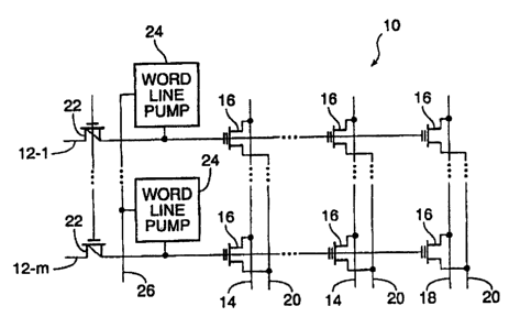
In a typical flash memory array, the memory cells are arranged in a
rectangular array of
rows and columns. Portions of a conventional flash memory array 10 are
depicted in FIG. 1.
In the flash memory array 10, wordlines 12 and bitlines 14 are arranged as a
matrix to form
intersections that have flash memory cells 16 disposed therein. A known flash
memory cell
suitable for use according to the present invention is described in United
States Patent No.
4,783,766, filed May 30, 1986, assigned to the same assignee as the present
invention, and
incorporated herein by reference.
Each wordline 12 in the flash memory array 10 represents one of M rows,
wherein each
of the M rows has N words. Each of the M rows in the flash memory array 10 is
typically
referred to as a page of memory. The number of bitlines 14 in the flash memory
array 10 is
approximately the same as the number of N words in a row multiplied by the
number of bits in
each word. For example, in the 4-Megabit Serial DataFlash'~"'' , part number
AT45DB041, by
Atmel Corporation, San Jose, CA, each row of a known 4M flash memory array 10,
there are
264 words each having 8 bits.
For each of the flash memory elements disposed at the intersection of a
wordline 12 and
a bit line 14, the drain of the flash memory element 16 is connected to the
bit line 14, the source
of the flash memory element 16 is connected to an array source voltage by an
array source line
20, and the gate of the flash memory element 16 is connected to the word line
12. For each of
the word lines 12, a P-channel MOS isolation pass transistor 22 is connected
in series between
wordline access circuitry (not shown) and the first flash memory element 16
disposed at the
intersection of the wordline 12 and a bit line 14. Connected to the portion of
each word line 12
disposed between P-channel MOS isolatian pass transistor 22 and the gate of
the first flash
memory element 16 in each row is a word line pump 24 connected to a source of
negative
voltage during erase of about -15 volts to about -4 volts, and preferably -10
volts, by word line
negative pump line 26.
SUBSTTTUTE SHEET (RULE 26)
CA 02341706 2001-02-26
WO 00/16338 PCTNS99/21018
The operations that may be performed on the memory cells in the flash memory
array
are PROGRAM, ERASE and READ. The PROGRAM operation is often performed by
driving selected bitlines 14 connected to the drain region in the flash memory
cells 16 to a first
voltage and driving the gates of the flash memory cells 16 connected to
selected wordlines 12 to
a second higher voltage to perform hot electron injection in a manner well
known to those of
ordinary skill in the art.
The ERASE operation is performed by driving the gate of the flash memory cell
16 to a
voltage that is substantially less than a voltage placed on the bitline 14. In
doing so, electrons
are tunneled off of the floating gate of the flash memory cell 16 in a manner
well known to
those of ordinary skill in the art. For a conventional flash memory array 10,
it is known that
ERASE operation may be a BULK ERASE wherein the entire flash memory array 10
is erased,
a SECTOR ERASE wherein a sector in the flash memory array 10 is erased, or a
PAGE
ERASE wherein an erase may be performed on a single row in a sector. By
constraining the
ERASE operation to either a SECTOR or BULK ERASE, the disturb phenomenon
associated
with the occurrence of unintended tunneling in unselected rows is reduced.
Although the erase disturb phenomenon can be reduced by the manner in which
the
ERASE operation is performed, an external refresh of the memory cells may be
performed as
described in the data sheet for the Atmel 4-Megabit Serial Dataflash~'~"''
part no. AT45DB041 for
disturbs cause by both erase and program operations. In the external refresh
an Auto Page
Rewrite corninand may be employed by the data flash user to refresh a row in
the flash memory
array by reading the data stored in the row into a buffer, and then writing
the data stored in the
buffer back into the same row. The Auto Page Rewrite command describing the
buffer write
operation is further disclosed in United States patent application , serial
No. 08/824,175 to
Gupta et al., filed March 26, 1997, entitled "Dual Buffer Flash Memory
Architecture With
Multiple Operating Modes", assigned to the same assignee as the present
application, and
expressly incorporated herein by reference. Performing the external refresh
with the Auto Page
Rewrite command requires the user of the flash memory array to provide the
instructions for
performing the Auto Page Rewrite and also to provide a sequentially
incremented page address
for row to be refreshed. Requiring the user to provide these instructions may
at times prove to
be cumbersome to the user of the flash memory array.
It is therefore an object of the present invention to provide an internal row
refresh for a
flash memory array that automatically scrolls through the rows in a flash
memory array to
refresh the memory cells of the flash memory array.
2
SUBSTITUTE SHEET (RULE 26)
CA 02341706 2001-02-26
WO 00/16338 PC'T/US99/21018
It is a further object of the present invention to provide an internal row
refresh for a flash
memory array that is programmable by the user to automatically scroll through
the rows in a
flash memory array to refresh one row of the memory cells after every Nth
erase and program
operation of the flash memory array.
BRIEF DESCRIPTION OF THE INVENTION
According to the present invention, an internal refresh periodically rewrites
the
information stored in each of the rows of memory cells in a flash memory. The
flash memory
array includes a refresh pointer bitline that indicates the row to be
refreshed.
In a first embodiment of the present invention, the internal refresh is
performed automatically
after every user erase/program cycle. In second and third embodiments, the
user of the flash
memory array selects when the internal refresh is performed, but the address
of the row to be
refreshed is supplied internally. In each of the three embodiments, the
internal refresh includes
the four operations of SCAN, REFRESH ERASE, REFRESH PROGRAM, and
INCREMENT.
In the first embodiment of the present invention, the SCAN operation of the
internal
refresh is followed by user erase/program cycle, the internal refresh
operation is then resumed
by performing the REFRESH ERASE, REFRESH PROGRAM, and INCREMENT
OPERATIONS.
In the second embodiment of the present invention, the user erase/program
cycle
includes the operation of POINTER READ and POINTER PROGRAM. These operations
check to see whether the row to be accessed in the user erase/program cycle is
also the next row
to be internally refreshed, and if so maintain the state of memory cell on the
refresh pointer
bitline after the user erase/program cycle. After a user erase/program cycle
selected by the user
of the flash memory array, the internal refresh is performed with the SCAN,
REFRESH
ERASE, REFRESH PROGRAM, and INCREMENT operations.
In the third embodiment of the present invention, a refresh select circuit is
included in
the flash memory array. With inclusion of the refresh select circuit, the
POINTER READ and
POINTER PROGRAM are not performed during each user erase/program cycle. After
a user
erase/program cycle selected by the user of the flash memory array, the
internal refresh is
performed with the SCAN, REFRESH ERASE, REFRESH PROGRAM, and INCREMENT
operations.
SUBSTITUTE SHEET {RULE 26)
CA 02341706 2001-02-26
WO 00/16338 PCT/US99/21018
BRIEF DESCRIPTION OF THE DRAWINGS
FIG. 1 is a portion of a known flash memory array suitable for use according
to the
present invention.
FIG. 2 is a bitline decoder circuit for a flash memory array suitable for use
according to
the present invention.
FIGS. 3A-3C are schematic diagrams of circuits for generating the YASCAN and
YBSCAN signals employed by the bitline decoder circuit of FIG. 2 according to
the present
invention.
FIG. 4 illustrates Tables I, II, and III indicating the signals employed
according to first,
second and third embodiments of the present invention
FIG. 5 is a schematic diagram of refresh select circuit suitable for use in a
flash memory
array according to a third embodiment of the present invention.
FIG. 6 is a schematic diagram of a pass gate circuit for generating the
PASSGATE and
PULLDOWN signals employed by the refresh select circuit of FIG. 5 according to
the third
embodiment of the present invention.
FIG. 7 is tables illustrating signals employed according to the third
embodiment of the
present invention.
FIG. 8 is a timing diagram of signals employed according to a third embodiment
of the
present invention.
DETAILED DESCRIPTION OF A PREFERRED EMBODIMENT
Those of ordinary skill in the art will realize that the following description
of the present
invention is illustrative only and not in any way limiting. Other embodiments
of the invention
will readily suggest themselves to such skilled persons.
According to the present invention, an internal refresh periodically rewrites
the
information stored in each of the rows of memory cells in a flash memory. The
refresh of the
present invention is referred to as "internal", because unlike the prior art,
the page address of
the page to be rewritten is not applied "externally" by the user of flash
memory array.
SUBSTITUTE SHEET (RULE 26)
CA 02341706 2001-02-26
WO 00/16338 PCTNS99/21018
Accordingly, in the present invention, in the memory array 10 of FIG. 1, there
is a bitline that is
a dedicated address or refresh pointer. The use of the refresh pointer bitline
will be described in
detail below. In the portion of the flash memory array 10 depicted in FIG. 1,
the refresh pointer
bitline is indicated by reference numeral 18. It should be appreciated that
the flash memory
array 10 depicted in FIG. 1 may represent an entire flash memory array or
simply a sector in a
flash memory array as is well understood by those of ordinary skill in the
art.
In a first embodiment of the present invention, the periodicity of the
internal refresh is
such that an internal refresh is performed after every user erase/program
cycle. In alternative
second and third embodiments of the present invention, the periodicity of the
internal refresh is
set by the user of the flash memory array such that an internal refresh is
performed in response
to a command by the user after a user erase/program cycle selected by the
user. For each of the
embodiments, internal refresh includes the four operations of SCAN, REFRESH
ERASE,
REFRESH PROGRAM, and INCREMENT.
In the SCAN operation, the memory cell 16 on the refresh pointer bitline 18
for each
row is read until a value of '0' is found. The row in the flash memory array
10 that has the '0'
value in the memory cell 16 on the refresh pointer bitline 18 will have the
data stored therein
refreshed by being rewritten. Also as part of the SCAN operation, the address
of the row to be
refreshed is stored in a scan latch. Before the REFRESH ERASE and REFRESH
PROGRAM
operations, the data in the row being refreshed is written to a buffer (not
shown). The row is
then erased by the REFRESH ERASE operation, and the data stored in the buffer
is written
back into the row by a REFRESH PROGRAM operation. In the INCREMENT operation,
the
row address in the scan latch is incremented to reflect the address of the
next row to be
refreshed, and the corresponding memory cell 16 on the refresh pointer bitline
18 for the next
row to be refreshed is written to a '0' by a PROGRAM operation.
Turning now to FIG. 2, an exemplary bit line decoder 40 that decodes the
bitlines of a
flash memory array 10 such as is depicted in FIG. 1, and is suitable for use
according to the
present invention is illustrated. It will be appreciated by those of ordinary
skill in the art that
other implementations of the bitline decoder 40 may be employed without
deviating from the
present invention disclosed herein. The bitline decoder 40 selects a word from
a selected row in
the flash memory 10 upon which to perform a desired operation, such as for
example, a READ
or PROGRAM. For the example illustrated in FIG. 2, the word width of the
selected word is
eight bits (BO-B7).
In the bit line decoder 40, each of the bit lines 14 in FIG. 1 is connected to
a first
source/drain of a separate N-channel MOS pass gate 42. The N-channel MOS pass
gates 42
SUBSTTTLTTE SHEET (RULE 26)
CA 02341706 2001-02-26
WO 00/16338 PCTNS99/21018
are grouped together such that the second source/drain of each of the N-
channel MOS pass
gates 42 in the same group are connected together to form a common node 44.
The gates of N-
channel MOS pass transistors 42 are coupled to the decode signals YA<O:m>.
Each common node 44 is connected to a first source/drain of an N-channel MOS
pass
transistor 46. The N-channel MOS pass transistors 46 are grouped such that the
second
source/drain of each of the N-channel MOS pass gates 46 in the same group are
connected
together to form a common node 48. The N-channel MOS pass transistors 46 are
connected by
the signals YB<O:n>. The common nodes 48-0 through 48-7 provide the I/O for
the word that
is being operated on in the flash memory array.
In the regular operation of the flash memory array 10, the YA<O:m> and YB<O:n>
select
a word in the selected row when a desired operation is to be performed. ~ In
the selection
process, one of the signals YA<O:m> will have a HIGH logic level to turn on
one of the N-
channel MOS transistors 42-0 through 42-m in each of the N groups. It should
be appreciated
from the bitline decoder that there will be eight sets (one group for each bit
in the eight bit wide
word being decoded) of N groups. A HIGH logic level from one of the YB<O:n>
signals will
simultaneously turn on one of the N-channel MOS transistors 46-0 through 46-n
to provide a
path through one of the N-channel MOS transistors 42-0 through 42-m that was
selected by the
YA<O:m> signals.
The refresh pointer bit line 18 of FIG. 1 is connected to first source/drain
of N-channel
MOS pass transistor 50 having a second source/drain connected to a first
source/drain of N-
channel MOS pass transistor 52. A second source/drain of N-channel MOS pass
transistor 52
is connected to common node 48-7. The gates of N-channel MOS pass transistors
50 and 52
are connected to the signals YASCAN and YBSCAN, respectively, that are
generated in
response to control signals to be described below. When an operation is to be
performed on the
memory cell 16 on the bitline 18 of a selected row, the YASCAN and YBSCAN
signals provide
a HIGH logic level to the gates of N-channel MOS pass transistors 50 and 52 to
turn them on.
FIGS. 3A, 3B and 3C schematically depict a COLUMN scan circuit 60, a YA scan
circuit 80 and a YB scan circuit 100, respectively, for generating the
COLUMNSCAN,
YASCAN, and YBSCAN signals in response to the control signals REWRITE MODE,
ERASE CYCLE, SCAN MODE, INCREMENT MODE, POINTER READ MODE, and
POINTER PROGRAM MODE. In the COLUMN scan circuit 60, a NAND gate 62 has a
first
input connected to the REWRITE MODE control signal and a second input
connected to the
ERASE CYCLE control signal, and a NOR gate 64 has a first input connected to a
SCAN
6
SUBST)rTUTE SHEET (RULE 26)
CA 02341706 2001-02-26
WO 00/16338 PCT/US99/21018
MODE control signal, a second input connected to an INCREMENT MODE control
signal, a
third input connected to an POINTER READ MODE control signal, and a fourth
input
connected to an POINTER PROGRAM MODE control signal.
The output of NAND gate 62 is connected through an inverter 66 to a first
input of
NOR gate 68, and the output of NOR gate 64 is connected through an inverter 70
to a second
input of NOR gate 68. The output from inverter 70 also forms the signal
YADISABLE. The
output of NOR gate 68 is fed through an inverter 72 to form the signal
COLUMNSCAN. The
COLUMNSCAN signal is coupled to both the YA and YB scan circuits 80 and 100,
respectively.
In the YA scan circuit 80 of FIG. 3B, the COLUMNSCAN signal is fed through
first
and second inverters 82 and 84 to the drain of N-channel MOS transistor 86.
The source of N-
channel MOS transistor 86 is connected to the source of P-channel MOS
transistor 88, the gate
of P-channel MOS transistor 90, and the gate of N-channel MOS transistor 92 to
form a
common node 94. The gate of N-channel MOS transistor 86 is coupled to voltage
source Vdd.
A variable voltage source, VMY, is coupled to the drain and bulk (backgate) of
P-channel MOS
transistors 88 and 90. The gate of P-channel MOS transistor 88 is connected to
a common
connection between the source of P-channel MOS transistor 90 and the drain of
N-channel
MOS transistor 92. The source of N-channel MOS transistor 92 is connected to
ground. The
signal YASCAN, coupled to the gate of N-channel MOS transistor 50 of FIG. 2,
is formed on
common node 94.
The YB scan circuit 100 of FIG. 3C is identical to the YA scan circuit 80 of
FIG. 3B.
Accordingly, in the YB scan circuit 100, the COLUMNSCAN signal is fed through
first and
second inverters 102 and 104 to the drain of N-channel MOS transistor 106. The
source of N-
channel MOS transistor 106 is connected to the source of P-channel MOS
transistor 108, the
gate of P-channel MOS transistor 110, and the gate of N-channel MOS transistor
112 to form a
common node 114. The gate of N-channel MOS transistor 106 is coupled to
voltage source
Vdd. A variable voltage source, VMY, is coupled to the drain and bulk
(backgate) of P-channel
MOS transistors 108 and 110. The gate of P-channel MOS transistor 108 is
connected to a
common connection between the source of P-channel MOS transistor 110 and the
drain of N-
channel MOS transistor 112. The source of N-channel MOS transistor 112 is
connected to
ground. The signal YBSCAN, coupled to the gate of N-channel MOS transistor 52
of FIG. 2,
is formed on common node 114.
Referring now to Table I in FIG. 4, the operation of the COLUMN scan circuit
60, YA
scan circuit 80, and YB scan circuit 100 according to a first embodiment of
the present will be
SUBSTITUTE SHEET (RULE 26)
CA 02341706 2001-02-26
WO 00/16338 _ PCT/US99/21018
described. The signals YASCAN, and YBSCAN illustrated in Table I are generated
in response
to the control signals ERASE CYCLE, SCAN MODE, and INCREMENT MODE and the
variable voltage level VMY. The control signals REWRITE MODE, POINTER READ
MODE,
and POINTER PROGRAM MODE are not employed in the first embodiment of the
present
invention, and as such may either be onutted, or in the case of the REWRITE
MODE control
signal be tied HIGH, and in the case of the POINTER READ MODE and POINTER
PROGRAM MODE control signals be tied LOW. .
According to Table I, for the internal refresh operation performed according
to the first
embodiment of the present invention in conjunction with each user
erase/program cycle, a
SCAN operation is first performed at step 120 prior to performance of the USER
ERASE and
USER PROGRAM operations, illustrated in steps 122 and i24, in the user
erase/program
cycle. In the SCAN operation, a HIGH logic level SCAN MODE signal is applied
to the first
input of NOR gate 64. Accordingly, a HIGH logic level COLUMN SCAN signal is
coupled
from the COLUMN scan circuit 60 to both the YA scan circuit 80, and YB scan
circuit 100.
In FIG. 3B, the HIGH logic level of the COLUMN SCAN signal is passed by N-
channel MOS pass transistor 86 to turn on N-channel MOS transistor 92. As a
result, the
ground voltage is applied to the gate of P-channel MOS transistor 88 to turn
it on and place the
variable voltage VMY, which during the SCAN operation is Vcc, onto the common
node 94 to
provide the YASCAN signal to the gate of N-channel MOS transistor 50 and
thereby turn it on.
The operation of YB scan circuit 100, in FIG. 3C to provide the YBSCAN signal
to the gate of
N-channel MOS transistor 52 and thereby turn it on is the same as that of the
YA scan circuit
80, just described.
During the SCAN operation, the HIGH logic level SCAN MODE signal also results
in
a HIGH YADISABLE signal. When the YADISABLE signal is HIGH a LOW logic level
is
applied to the gates of N-channel MOS transistors 42-0 through 42-m of FIG. 2
to prevent any
of the other memory cells 16 in the flash memory array 10 from being read. The
signal applied
to the gates of the N-channel MOS pass transistors 46 is a don't care. Once a
'0' value has
been read from a memory cell 16 in the refresh pointer column 18, the address
of the row in
which the memory cell 16 is disposed is stored in a scan latch. A scan latch
suitable for storing
the row address is within the level of skill of those of ordinary skill in the
art and will not be
described herein to avoid overcomplicating the disclosure and thereby
obscuring the present
invention.
SU8STTTUTE SHEET (RULE 26)
CA 02341706 2001-02-26
WO 00/16338 PCT/US99/Z1018
At steps 122 and 124 the operations of USER ERASE and USER PROGRAM,
respectively, are performed on the row selected by the user. To do so, at step
122 the SCAN
MODE signal is brought LOW, and the ERASE CYCLE signal is brought HIGH. As
mentioned above, in the first embodiment of the present invention described
herein, the
REWRITE MODE signal is not required. As a consequence, the COLUMN SCAN signal
is
HIGH, and as in step 120, the variable voltage level VMY appears on common
nodes 94 and
114 of the YA scan circuit 80, and YB scan circuit 100, respectively. However,
unlike step 120,
the variable voltage level VMY is 10 volts rather than Vcc to properly turn on
the N-channel
MOS transistors 50 and 52 during the USER ERASE operation. Also during the
USER
ERASE operation, each of the N-channel MOS transistors 42 and 46 is turned on
so that entire
selected row is erased.
At step 124 the ERASE CYCLE signal makes a transition from HIGH to LOW, and
the
SCAN MODE and INCREMENT MODE signals are kept LOW. As mentioned above, in the
first embodiment of the present invention described herein, the POINTER READ
MODE and
POINTER PROGRAM MODE control signals are not required. As a result, the
outputs of
both the NAND gate 62 and the NOR gate 64 are both HIGH. These HIGH signals
are fed
through inverter 66 and 70 to the first and second inputs of NOR gate 68. The
HIGH output of
NOR gate 68 is fed through inverter 72 so that the COLUMNSCAN signal is LOW.
In YA scan circuit 80, the LOW COLUMN SCAN signal is fed through inverters 82
and 84 and passed by N-channel MOS transistor 86 to node 94 where it is
latched by P-channel
MOS transistors 88 and 90, and N-channel MOS transistor 92. The operation of
the YBSCAN
circuit 100 is the same as the operation of the YASCAN circuit just described.
With the
YASCAN and YBSCAN signals both LOW, the N-channel MOS transistors 50 and 52
are
both turned off. As a result, the memory cell 16 on the refresh pointer bit
line 18 which was
erased at step 122 cannot now be programmed. The YA and YB signals which
properly decode
the portions of the row that the user wishes to program into the flash memory
array 10 are also
provided at step 124.
At steps 126 and 128, the internal refresh operation that began with the SCAN
operation
at step 120 is continued. The REFRESH ERASE and REFRESH PROGRAM operations at
steps 126 and 128 are similar to the USER ERASE and USER PROGRAM operations
steps
122 and 124, with the exception that the row upon which the operations are
being performed
corresponds to the row address latched in the scan latch during the SCAN
operation of step
120. Prior to REFRESH ERASE at step 126, the row to be refreshed is first
written into a
SUBSTITUTE SHEET (RULE Z6)
CA 02341706 2001-02-26
WO 00/16338 PCT/US99/21018
buffer. At step 126, the ERASE CYCLE signal is brought HIGH. As previously
described, the
COLUMNSCAN signal will go HIGH as a result.
With the COLUMNSCAN signal HIGH and the variable voltage VMY at 10 volts, the
voltage at nodes 94 and 114 of YA scan and YB scan circuits 80 and 100,
respectively, that form
the YASCAN and YBSCAN signals are also at 10 volts. Further, the YA and YB
decode signals
turn on all of the N-channel MOS transistors 42 and 46. Since all of the
transistors in the
decoder 40 illustrated in FIG. 2 are turned on, the row at the selected
address is completely
erased. At step 128, the ERASE CYCLE signal is brought LOW. As a result, the
data stored in
the buffer is rewritten to the selected row in the same manner as the USER
PROGRAM
operation that occurred at step 124.
At step 130, the internal refresh cycle is completed with the INCREMENT
operation. In
the INCREMENT operation, the row address latched in the scan latch is
incremented and the
memory cell 16 on the refresh pointer bit line 18 corresponding to the
incremented row address
is programmed to a value of '0'. At step 130, the INCREMENT MODE signal is
brought
HIGH, and as a result, the COLUMNSCAN signal is also HIGH. With the COLUMN
SCAN
signal HIGH, and the variable voltage VMY at 10 volts, the common nodes 94 and
114 in YA
scan and YB scan circuits 80 and 100, respectively, forming the YASCAN and
YBSCAN
signals, and coupled to N-channel MOS transistors 50 and 52, are set at 10
volts for the
program operation. The YA signals provided to the bit line decode circuit 40
in FIG. 2 are all
set to a LOW voltage level so that none of the other bits in the selected row
are programmed.
According to the second and third embodiments of the present invention, the
user of the
flash memory array 10 may set the periodicity of the internal refresh so that
the internal refresh
is performed after a user erase/program cycle as desired by providing an
"internal refresh
command" to the flash memory array 10. Unlike the prior art, the address of
the row to be
refreshed is not provided by the user, but rather, is kept track of by the
flash memory array 10
and provided internally by the flash memory array 10.
In the second embodiment of the present invention, the SCAN, REFRESH ERASE,
REFRESH PROGRAM, and INCREMENT operations of the internal refresh are
implemented
with the COLUMN scan circuit 60, the YA scan circuit 80, and YB scan circuit
100 in response
to the ERASE CYCLE, SCAN MODE, INCREMENT MODE, POINTER READ MODE and
POINTER PROGRAM MODE control signals. The YA, YB, YASCAN, and YBSCAN
signals, and variable voltage VMY associated with the second embodiment of the
present
invention are illustrated in Table II of FIG. 4.
SUBSTITUTE SHEET (RULE 26)
CA 02341706 2001-02-26
WO 00/16338 PCT/US99/21018
In Table II, the user program/erase cycle including the POINTER READ, USER
ERASE, USER PROGRAM, and POINTER PROGRAM operations is depicted at steps 140,
142, 144, and 146, and an internal refresh including the SCAN, REFRESH ERASE,
REFRESH
PROGRAM, and INCREMENT performed after a selected user program/erase cycle is
depicted at steps 148, 150, 152 and 154.
In the second embodiment of the present invention, at step 140, during each
user
erase/program cycle, a POINTER READ of the memory cell 16 on the refresh
pointer bitline 18
of the row to be erased and programmed is performed. In the POINTER READ
operation, a
HIGH logic level POINTER READ MODE signal is applied to the third input of NOR
gate 64.
Accordingly, a HIGH logic level COLUMN SCAN signal is coupled from the COLUMN
scan
circuit 60 to both the YA scan circuit 80, and YB scan circuit 100.
In FIG. 3B, the HIGH logic level of the COLUMN SCAN signal is passed by N-
channel MOS pass transistor 86 to turn on N-channel MOS transistor 92. As a
result, the
ground voltage is applied to the gate of P-channel MOS transistor 88 to turn
it on and place the
variable voltage VMY, which during the POINTER READ operation is Vcc, onto the
common
node 94 to provide the YASCAN signal to the gate of N-channel MOS transistor
50 and
thereby turn it on. The operation of YB scan circuit 100, in FIG. 3C to
provide the YBSCAN
signal to the gate of N-channel MOS transistor 52 and thereby turn it on is
the same as that of
the YA scan circuit 80, just described.
During the POINTER READ operation, the HIGH logic level POINTER READ
MODE signal also results in a HIGH YADISABLE signal. When the YADISABLE signal
is
HIGH a LOW logic level is applied to the gates of N-channel MOS transistors 42-
0 through
42-m of FIG. 2 to prevent any of the other memory cells 16 in the flash memory
array 10 from
being read. The signal applied tv the gates of the N-channel MOS pass
transistors 46 is a don't
care. When the contents of the memory cell being read during the POINTER READ
operation
are in programmed state, conventionally '0', an internal POINTER READ FLAG in
the flash
memory is set. The setting of flags is well understood by those of ordinary
skill in the art and
will not be further described herein.
At steps 142 and 144, the controls signals for performing the USER ERASE and
USER
PROGRAM operations are asserted as described above in steps I22 and 124 in the
first
embodiment of the present invention so that desired row is erased and
programmed. After the
completion of steps 142 and 144, when the POINTER READ FLAG is in a set state,
the
SUBSTITUTE SHEET (RULE 26)
CA 02341706 2001-02-26
WO 00/16338 PCT/US99/21018
POINTER PROGRAM operation at step i46 is performed. In the POINTER PROGRAM
operation the memory cell 16 on the refresh pointer bit line 18 corresponding
to either the row
just read and programmed by the user or an incremented row selected as a
matter of program
design choice by the user is programmed to a value of '0'.
At step 146, in the POINTER PROGRAM operation, a HIGH logic level POINTER
PROGRAM MODE signal is applied to the fourth input of NOR gate 64, and as a
result, the
COLUMNSCAN signal is also HIGH. With the COLUMN SCAN signal HIGH, and the
variable voltage VMY at 10 volts, the common nodes 94 and 114 in YA scan and
YB scan
circuits 80 and 100, respectively, forming the YASCAN and YBSCAN signals, and
coupled to
N-channel MOS transistors 50 and 52, are set at 10 volts for the program
operation. The YA
signals provided to the bit line decode circuit 40 in FIG. 2 are all set to a
LOW voltage level so
that none of the other bits in the selected row are programmed.
The internal refresh steps 148, 150, 152, and 154, in the second embodiment of
the
present invention are performed in the same manner as the internal refresh
steps 120, 126, 128,
and 130 in the first embodiment of the present invention.
In the third embodiment of the present invention, the SCAN, REFRESH ERASE,
REFRESH PROGRAM, and INCREMENT operations of the internal refresh are
implemented
with the COLUMN scan circuit 60, the YA scan circuit 80, and YB scan circuit
100 in response
to the REWRITE MODE, ERASE CYCLE, SCAN MODE, and INCREMENT MODE control
signals and the variable voltage VMY. The YA, YB, YASCAN, and YBSCAN signals,
and
variable voltage VMY associated with the third embodiment of the present
invention are
illustrated in Table III of FIG. 4.
In Table III, the user program/erase cycle including the USER ERASE and USER
PROGRAM operations is depicted at steps 156 and 158, and an internal refresh
including the
SCAN, REFRESH ERASE, REFRESH PROGRAM, and INCREMENT performed after a
selected user program/erase cycle is depicted at steps 160, 162, 164, and 166.
It should be
observed that the USER PROGRAM step 158 is the same as the USER PROGRAM step
144,
but that USER ERASE step 156 is different from the USER ERASE step 142.
In the third embodiment of the present invention, the POINTER READ and POINTER
PROGRAM operations in the user erase/program cycle of the second embodiment of
the
present invention are not employed, while the REWRITE MODE control signal is
employed.
In the USER ERASE operation at step 156 the REWRITE MODE control signal
coupled to he
l2
SUBSTITUTE SHEET (RULE 26)
CA 02341706 2001-02-26
WO 00116338 PCT/US99/21018
first input of NAND gate 62 is kept LOW. With the SCAN MODE and INCREMENT
MODE signals also LOW, the COLUMNSCAN signal is also LOW. As a result, the
YASCAN and YBSCAN signals are also LOW.
The operation of the internal refresh steps 160, 162, 164, and 166 in the
third
embodiment of the present invention is similar to the operation of the
internal refresh steps 120,
126, 128, and 130 in the first embodiment of the present invention, with the
exception that the
REWRITE MODE control signal is asserted during the REFRESH ERASE and REFRESH
PROGRAM operations.
It should be appreciated that in each of the three embodiments, when a HIGH
signal is
applied the gates of N-channel MOS transistors 42 and 46 by the signals YA and
YB,
respectively, the voltage applied to the gates of N-channel MOS transistors 42
and 46 is the
variable voltage VMY.
In the third embodiment of the present invention, the flash memory array 10 of
FIG. 1 is
modified to include a refresh select circuit. The refresh select circuit is
included so that the
internal refresh may be performed after a user erase/program cycle as desired
without
employing the POINTER READ and POINTER PROGRAM operations in the user
erase/program cycle of the third embodiment of the present invention.
Turning now to FIG. 5 the refresh select circuit 170 employed in the third
embodiment
of the present invention is illustrated. In the refresh select circuit 170,
there is disposed in each
of the exemplary first and second wordlines 12-1 and 12-2, between the memory
cells 16 on the
last bitline 14 in the flash memory array 10 and the memory cells 16 on the
refresh pointer
bitline 18, a P-channel MOS pass transistor 172 and a P-channel MOS pull-down
transistor
174. It should be appreciated that the P-channel MOS pass transistor 172 and a
P-channel
MOS pull-down transistor 174 are provided in each of the row of the flash
memory array 10 in
a similar manner.
In each row the drain of the P-channel MOS pass transistor 172 is coupled to
the
wordline 12, and the source of the P-channel MOS pass transistor 172 is
coupled to the
memory cell 16 on the refresh pointer bitline 18. A PASSGATE signal generated
by a pass
gate circuit to be described below is connected to the gate of each P-channel
MOS pass
transistor 172. The source of the P-channel MOS pass transistor 172 is also
coupled to the
drain of P-channel MOS pull-down transistor 174. The source of P-channel pull-
down
13
SUBSTITUTE SHEET (RULE 26)
CA 02341706 2001-02-26
WO 00/16338 PCTNS99/21018
transistor 174 is coupled to ground, and the gate of each P-channel pull-down
transistor 174 is
couple to a PULLDOWN signal generated by the pass gate circuit to be described
below.
In FIG. 6, a pass gate circuit 200 that generates the PASSGATE and PULLDOWN
signals in response to the control signals INTERNAL REFRESH, PROGRAM CYCLE,
ERASE CYCLE, ERASE/PROGRAM RESET and RESET, and the bias voltages VM, VMP,
NVM, and VWG is illustrated. In pass gate circuit 200, the INTERNAL REFRESH
control
signal is connected through an inverter 202 to a first input of NAND gate 204
and also to the
first input of a NAND gate 206. A second input of NAND gate 204 is connected
to the
PROGRAM CYCLE control signal, and a second input of NAND gate 206 is connected
to the
ERASE CYCLE control signal. The PROGRAM CYCLE control signal is also connected
through inverter 208 to the gate of N-channel MOS transistor 210, and the
ERASE CYCLE
control signal is also connected to a first input of NOR gate 212 and a first
input of NAND gate
214 through an inverter 216. The ERASE/PROGRAM RESET control signal is
connected to a
first input of a NOR gate 218, and the RESET control signal is connected to a
second input of a
NOR gate 218. The output of NAND gate 204 is connected through an inverter 220
to a third
input of NOR gate 218 and also to a second input of NOR gate 212 and a second
input of
NAND gate 214.
The output of NOR gate 218 is connected to the drain of N-channel MOS pass
transistor 222, and the gates of N-channel MOS transistors 224 and 226. The
gate of N-
channel MOS pass transistor 222 is connected to the voltage source Vdd. The
source of N-
channel MOS pass transistor 222 is connected to the source of P-channel MOS
transistor 228,
the gate of P-channel MOS transistor 230, and the gate of P-channel MOS
transistor 232. The
drains and buck (backgate) of P-channel MOS transistors 228, 230, and 232 are
connected to
source of diode connected N-channel MOS transistor 234. The gate and drain of
N-channel
MOS transistor 234 are connected to the variable voltage supply VM. The gate
of P-channel
MOS transistor 228 and the source of P-channel MOS transistor 230 are
connected to the drain
of N-channel MOS transistor 224. The source of P-channel MOS transistor 232 is
connected
to the drain of N-channel MOS transistor 226. The sources of N-channel MOS
transistors 224
and 226 are connected to ground. The common connection of the source of P-
channel MOS
transistor 232 and the drain of N-channel MOS transistor 226 are connected to
the drain of a P-
channel MOS transistor pass gate 236. The gate of P-channel MOS transistor 236
is connected
to ground.
The output of NAND gate 206 is connected through an inverter 238 to a first
input of
NAND gates 240 and 242. A second input of NAND gate 240 is connected to an
INTERNAL
14
SUBSTTTUTE SHEET {RULE 26)
CA 02341706 2001-02-26
WO 00/16338 PCTNS99/21018
CLOCK OSCILLATOR, and the output of NAND gate 240 is connected to a second
input of
NAND gate 242 and through capacitor 244 to the gate and drain of P-channel MOS
transistor
246, and the source of P-channel MOS transistor 248. The output of NAND gate
242 is
connected through capacitor 250 to the source of P-channel MOS transistor 246,
the gate of P-
channel MOS transistor 248, the source of a P-channel MOS transistor 252, and
the gate and
drain of a P-channel MOS transistor 254. A NEGATIVE VOLTAGE MULTIPLIER (NVM)
bias is connected to the drains of P-channel MOS transistors 248' and 252.
A drain of N-channel MOS transistor 210 is connected to the source of P-
channel MOS
transistor 256. The source of N-channel MOS transistor 210 and the gate of
Pchannel MOS
transistor 256 are both connected to ground. The backgates of P-channel MOS
transistors 256,
254, 252, 248, 246, and 236 are all connected to the common connection of the
source of P-
channel MOS transistor 232, the drain of N-channel MOS transistor 226 and the
drain of P-
channei MOS transistor pass gate 236. Also connected to this common connection
are the
gates and backgates of P-channel MOS transistors 258, 260, 262 and 264, and
the backgates of
P-channel MOS transistors 266, 268, 270, 272, 274, 276, 278 and 280.
The drains of P-channel MOS transistors 258, 260, 262 and 264 are coupled to
ground,
and the sources of P-channel MOS transistors 258, 260, 262 and 264 are
connected to the
drains and gates of P-channel MOS transistors 266, 268, 270 and 272,
respectively, and to a
first plate of capacitors 282, 284, 286 and 288, respectively. The sources of
P-channel MOS
transistors 260, 262 and 264 are also connected to the sources of P-channel
MOS transistors
266, 268 and 270, respectively. The source of P-channel MOS transistors 272 is
connected to
the drains and gates of P-channel MOS transistors 274 and 280. The source of P-
channel
MOS transistors 274 is connected to the gate and drain of P-channel MOS
transistor 276, the
source of P-channel MOS transistors 276 is connected to the gate and drain of
P-channel MOS
transistor 278, and the source of P-channel MOS transistors 278 is connected
to ground.
The INTERNAL REFRESH control signal is also connected through an inverter 290
to
a first input of a NOR gate 292. A second input of NOR gate 292 to the
ERASE/PROGRAM
RESET control signal, and the output of NOR gate 292 is connected to a first
input of NAND
gate 294 and a first input of NAND gate 296. A second input of NAND gate 294
is connected
to the INTERNAL CLOCK OSCILLATOR, and the output of NAND gate 294 is connected
to
a second input of NAND gate 296 and a second plate of capacitors 282 and 286.
The output of
NAND gate 296 is connected to a second plate of capacitors 284 and 288.
The source of P-channel MOS transistor 236, the gate of P-channel MOS
transistor
252, the source of P-channel MOS transistor 254, the drain of P-channel MOS
transistor 256
SUBSTITiJTE SHEET (RULE 26)
CA 02341706 2001-02-26
WO 00/16338 PC'fNS99/21018
and the source of P-channel MOS transistor 280 are connected at a common node
that forms
the PASSGATE signal of pass gate circuit 200.
The output of NAND gate 214 is connected to the drain of N-channel MOS
transistor
298 and the gate of N-channel MOS transistor 300. The source of N-channel MOS
transistor
298 is connected to the source of P-channel MOS transistor 302, the gate of P-
channel MOS
transistor 304, and the gate of P-channel MOS transistor 306. A variable
voltage source, VMP,
is coupled to drain and bulk (backgate) of P-channel MOS transistors 302, 304
and 306. The
gate of P-channel MOS transistor 302, the source of P-channel MOS transistor
304, and the
drain of N-channel MOS transistor 300 form a common connection. The source of
N-channel
MOS transistor 300 is coupled to ground.
The output of NOR gate 212 is coupled to the gate of an N-channel MOS
transistor
308. The source of N-channel MOS transistor 308 is coupled to ground, and the
drain of N-
channel MOS transistor 308 is connected to the source of P-channel MOS
transistor 306. The
gate of an N-channel MOS transistor 310 is coupled to the ERASE CYCLE control
signal, and
the drain of N-channel MOS transistor 310 is coupled to the variable bias
voltage VWG. The
common connection of the drain of Nchannel MOS transistors 308, the source of
N-channel
MOS transistor 310, and the source of P-channel MOS transistors 306 form the
PULL
DOWN signal of pass gate circuit 200.
In FIG. 8, Table IV illustrates the voltages of the PASSGATE and PULLDOWN
signals for various modes according to the present invention, and Table V
illustrates the voltages
of the voltage supplies VM, VMP, VWG, and NVM for various modes according to
the present
invention.
With regard to the passgate circuit 200 in FIG. 7, for the operation of the
third
embodiment of the present invention, when the internal refresh operation is
performed as shown
in the SCAN, REFRESH ERASE, REFRESH PROGRAM and INCREMENT operations at
steps 160, 162, 164 and 166 depicted in Table III of FIG. 4, the control
signal INTERNAL
REFRESH applied to pass gate circuit 200 will be a HIGH logic level, and when
the user
ERASE and PROGRAM cycle operations are performed as shown in the USER ERASE
and
USER PROGRAM operations at steps 156 and 158 in Table III of FIG. 4, the
control signal
INTERNAL REFRESH applied to the pass gate circuit 200 will be a LOW logic
level.
During the SCAN operation, the control signals ERASE CYCLE and PROGRAM
CYCLE will both be at a LOW logic level. As a result, the PASSGATE signal
applied to the
16
SUBSTTTUTE SHEET (RULE 26)
CA 02341706 2001-02-26
WO 00/16338 PCT/US99/Z1018
gates of P-channel MOS pass transistors 172 of FIG. 5 is -2 volts, and the
PULLDOWN
signal applied to the gates of P-channel MOS pull-down transistors 174 of FIG.
5 is
approximately 5 volts (VMP).
During the REFRESH ERASE operation, the control signal ERASE CYCLE will be
HIGH and the control signal PROGRAM CYCLE will be at a LOW as shown at
reference
numeral 350 in FIG. 8. As a result, the PASSGATE signal applied to the gates
of P-channel
MOS pass transistors 172 of FIG. 5 is approximately -10 volts, and the
PULLDOWN signal
applied to the gates of P-channel MOS pull-down transistors 174 of FIG. 5 is
approximately
1.5 volts (VWG).
During the REFRESH PROGRAM operation, the control signal ERASE CYCLE will
be LOW and the control signal PROGRAM CYCLE will be HIGH as shown at reference
numeral 352 in FIG. 8. The ERASE/PROGRAM RESET control signal will also
briefly pulse
HIGH as shown at reference numeral 354. As a result, the PASSGATE signal
applied to the
gates of P-channel MOS pass transistors 172 of FIG. 5 is -2 volts, and the
PULLDOWN
signal applied to the gates of P-channel MOS pull-down transistors 174 of FIG.
5 is
approximately 10 volts (VMP).
During the INCREMENT operation, the control signal ERASE CYCLE will be LOW
and the control signal PROGRAM CYCLE will be HIGH. As a result, the PASSGATE
signal
applied to the gates of P-channel MOS pass transistors 172 of FiG. 5 is -2
volts, and the
PULLDOWN signal applied to the gates of P-channel MOS pull-down transistors
174 of FIG.
is approximately 10 volts (VMP). At the end of the INCREMENT operation, the
RESET
control signal will briefly pulse HIGH as shown at reference numeral 356 to
reset the pass gate
circuit 200.
During the USER ERASE operation with the INTERNAL REFRESH control signal
LOW, the control signal ERASE CYCLE will be HIGH and the control signal
PROGRAM
CYCLE will be at a LOW as shown at reference numeral 350 in FIG. 8. As a
result, the
PASSGATE signal applied to the gates of P-channel MOS pass transistors 172 of
FIG. 5 is
less than 1 volt, and the PULLDOWN signal applied to the gates of P-channel
MOS pull-down
transistors 174 of FIG. 5 is approximately 1.5 volts (VWG).
During the USER PROGRAM operation with the INTERNAL REFRESH control
signal LOW, the control signal ERASE CYCLE will be LOW and the control signal
PROGRAM CYCLE will be HIGH as shown at reference numeral 352 in FIG. 8. The
17
SUBSTITUTE SHEET (RULE Z6)
CA 02341706 2001-02-26
WO 00/16338 PCTNS99/21018
ERASE/PROGRAM RESET control signal will also briefly pulse HIGH as shown at
reference
numeral 354 As a result, the PASSGATE signal applied to the gates of P-channel
MOS pass
transistors 172 of FIG. 5 is approximately 10 volts, and the PULLDOWN signal
applied to the
gates of P-channel MOS pull-down transistors 174 of FIG. 5 is approximately 0
volts.
While embodiments and applications of this invention have been shown and
described, it
would be apparent to those slciiled in the art that many more modifications
than mentioned
above are possible without departing from the inventive concepts herein. The
invention,
therefore, is not to be restricted except in the spirit of the appended
claims.
~8
SUBSTITUTE SHEET (RULE 26)