Note: Descriptions are shown in the official language in which they were submitted.
CA 02341735 2001-02-26
WO 00/17892 PCT/US99/21899
1
OVERVOLTAGE PROTECTION DEVICE INCLUDING
WAFER OF VARISTOR MATERIAL
Field of the Invention
S The present invention relates to voltage surge protection
devices and, more particularly, to a voltage surge protection
device including a wafer of varistor material.
Background of the Invention
Frequently, excessive voltage is applied across service
lines which deliver power to residences and commercial and
institutional facilities. Such excess voltage or voltage spikes
may result from lightning strikes, for example. The voltage
surges are of particular concern in telecommunications
distribution centers, hospitals and other facilities where
equipment damage caused by voltage surges and resulting down time
may be very costly.
Typically, one or more varistors (i.e., voltage dependent
resistors) are used to protect a facility from voltage surges.
Generally, the varistor is connected directly across an AC input
and in parallel with the protected circuit. The varistor has a
characteristic clamping voltage such that, responsive to a
voltage increase beyond a prescribed voltage, the varistor forms
a low resistance shunt path for the overvoltage current that
reduces the potential far damage to the sensitive components.
Typically, a line fuse may be provided in the protective circuit
and this line fuse is blown or weakened by the essentially short
circuit created by the shunt path.
Varistors have been constructed according to several designs
for different applications. For heavy duty applications (e. g.,
surge current capability in the range df from about 60 to 100 kA)
such as protection of telecommunications facilities, block
varistors are commonly employed. A block varistor typically
includes a disk shaped varistor element potted in a plastic
housing. The varistor disk is formed by pressure casting a metal
CA 02341735 2006-02-17
2
oxide material, such as zinc oxide, or other suitable
material such as silicon carbide. Copper, or other
electrically conductive material, is flame sprayed onto
the opposed surfaces of the disk. Ring shaped electrodes
are bonded to the coated opposed surfaces and the disk
and electrode assembly is enclosed within the plastic
housing. Examples of such block varistors include Product
No. SIOV-B860K250 available from Siemens Matsushita
Components GmbH & Co. KG and Product No. V271BA60
available from Harris Corporation.
Another varistor design includes a high energy
varistor disk housed in a disk diode case. The diode case
has opposed electrode plates and the varistor disk is
positioned therebetween. One or both of the electrodes
include a spring member disposed between the electrode
plate and the varistor disk to hold the varistor disk in
place. The spring member or members provide only a
relatively small area of contact with the varistor disk.
The varistor constructions described above often
perform inadequately in service. Often, the varistors
overheat and catch fire. Overheating may cause the
electrodes to separate from the varistor disk, causing
arcing and further fire hazard. There may be a tendency
for pinholing of the varistor disk to occur, in turn
causing the varistor to perform outside of its specified
range. During high current impulses, varistor disks of
the prior art may crack due to piezoelectric effect,
thereby degrading performance. Failure of such varistors
has led to new governmental regulations for minimum
performance specifications. Manufacturers of varistors
have found these new regulations difficult to meet.
CA 02341735 2006-02-17
3
Summary of the Invention
In accordance with one aspect of the invention,
there is provided an overvoltage protection device
including a housing including a first substantially
planar electrical contact surface and an electrically
conductive, metal sidewall, the housing defining a cavity
therein and having an opening in communication with the
cavity. The overvoltage protection device also includes
an electrode member including a substantially planar
second electrical contact surface facing the first
electrical contact surface and disposed within the
cavity, a portion of the electrode extending out of the
cavity and through the opening. The overvoltage
protection device further includes a wafer formed of
varistor material and having first and second opposed,
substantially planar wafer surfaces, the wafer positioned
within the cavity and between the first and second
electrical contact surfaces with the first and second
wafer surfaces engaging and in electrical contact with
the first and second electrical contact surfaces,
respectively. In response to an overvoltage surge
condition between the housing and the electrode, the
wafer provides a shunt path for surge current, thereby
preventing an overvoltage condition between the housing
and the electrode.
The first and second electrical contact surfaces may
apply a load to the first and second wafer surfaces.
The load may be at least 264 lbs.
The load may be between about 528 and 1056 lbs.
The device may further include adjustable means
maintaining the load such that the amount of the load may
be selectively adjusted.
CA 02341735 2006-02-17
4
The device may further include biasing means for
maintaining the load.
The biasing means may include a spring member biasing
at least one of the first and second electrical contact
surfaces against the wafer.
The device may further include a plurality of spring
members biasing at least one of the first and second
electrode
members
against
the wafer.
The spring member may include a spring washer.
The spring member may include a Belleville washer.
The device may further include an end cap positioned
in the opening,
the end
cap maintaining
the load.
The device may further include a clip operative to
limit di splacement between the end cap and the housing
to
maintain the load.
The housing may include a slot formed therein and
the clip engages the slot.
The housing may include a threaded portion and the
end cap may include a threaded portion engaging the
housing threaded portion whereby the end cap may be
operable to selectively adjust and maintain the load.
The device may further include a spring member
interpos ed between the end cap and the wafer.
The device may further include an electrically
insulating
member
interposed
between
the second
contact
surface and the opening.
The device may further include an end cap positioned
in the opening and having a hole formed therein. The
electrod e member may include a head positioned in the
cavity between
the end
cap and
the first
electrical
contact surface and a shaft extending out of the cavity
and through
the end
cap hole.
CA 02341735 2006-02-17
4a
The device may further include an electrically
insulating ring member having a hole formed therein, the
insulating ring member interposed between the head and
the end cap and the shaft may extend through the
insulating ring member hole.
The insulating ring member may include a main body
ring portion and a projecting collar, the projecting
collar surrounding the shaft and extending through the
end cap hole.
The device may further include a spring washer having
a hole formed therein, the spring washer interposed
between the head and the end cap and the shaft may extend
through the spring washer hole.
The device may include an electrically insulating
ring member and a spring washer, the electrically
insulating ring member having a hole formed therein and
interposed between head and the end cap, the spring washer
having a hole formed therein and interposed between head
and the electrically insulating ring member, the shaft
extending through each of the electrically insulating ring
member hole and the spring washer hole.
The housing and the electrode member may have a
combined thermal mass which is substantially greater than
a thermal mass of the wafer.
The housing may include an electrode wall and second
electrode member may include a head, each of the
electrode wall and the head contacting one of the wafer
surfaces and having a thermal mass which is substantially
greater than the wafer thermal mass.
The thermal masses of the electrode wall and the
head may be each at least twice the wafer thermal mass.
The thermal masses of the electrode wall and the head
may be each at least ten times the wafer thermal mass.
CA 02341735 2006-02-17
4b
The housing may be unitarily formed of metal.
The wafer may be formed by slicing a rod of varistor
material.
The rod may be formed by at least one of extruding
and casting.
The varistor material may be selected from the group
consisting of a metal oxide compound and silicon carbide.
The wafer may include a coating of conductive metal
on at least one of the first and second wafer surfaces.
The wafer may have a substantially circular
peripheral edge and each of the first and second disk
surfaces may be substantially coextensive with the
circular peripheral edge.
Each of the first and second contact surfaces may be
continuous and substantially free of voids.
In accordance with another aspect of the invention,
there is provided an overvoltage protection device
including a housing including an electrode wall and an
electrically conductive, metal sidewall, the electrode
wall and the sidewall defining a cavity and an opening in
communication with the cavity, the electrode wall having a
thermal mass and a first substantially planar electrical
contact surface. The overvoltage protection device also
includes an electrode member including a head positioned
in the cavity and a shaft extending out of the cavity and
through the opening, the head having a thermal mass and a
substantially planar second electrical contact surface
facing the first electrical contact surface. The
overvoltage protection device further includes a wafer
formed of varistor material and having first and second
opposed, substantially planar wafer surfaces, the wafer
positioned within the cavity and between the first and
second electrical contact surfaces with the first and
CA 02341735 2006-02-17
4c
second wafer surfaces engaging the first and second
electrical contact surfaces, respectively, the wafer
having a thermal mass. The overvoltage protection device
also includes an end cap positioned in the opening, the
end cap having a hole through which the shaft extends. The
overvoltage protection device further includes a spring
member interposed between the end cap and the head, and
the spring member biasing at least one of electrode wall
and the head against the wafer to apply a load to the
first and second wafer surfaces. Each of the head thermal
mass and the electrode wall thermal mass is substantially
greater than the thermal mass of the wafer.
The load may be at least 264 lbs.
The thermal masses of the electrode wall and the
head may be each at least ten times the wafer thermal
mass.
The wafer may be formed by slicing a rod of the
varistor material.
The device may further include a clip and the housing
may include a slot formed therein. The clip may be
cooperative with the slot to limit displacement of the end
cap relative to the housing and to maintain the load.
The housing may include a threaded portion and the
end cap may include a threaded portion engaging the
housing threaded portion whereby the end cap may be
operable to selectively adjust and maintain the load.
The device may further include an electrically
insulating ring member, the insulator ring member having
a hole formed therein and interposed between the head and
the end cap, the spring member having a hole formed
therein and interposed between head and the insulating
ring member whereby the spring member biases the head
against the wafer, and the shaft may extend through each
CA 02341735 2006-02-17
4d
of the insulating ring member hole and the spring member
hole.
The insulating ring member may include a main body
ring portion and a projecting collar, the projecting
collar surrounding the shaft and extending through the end
cap hole.
In accordance with another aspect of the invention,
there is provided an overvoltage protection device for
use with a varistor wafer of the type having first and
second opposed, substantially planar wafer surfaces. The
device includes a housing including a first substantially
planar electrical contact surface and an electrically
conductive, metal sidewall, the housing defining a cavity
therein and having an opening in communication with the
cavity. The device also includes an electrode member
including a substantially planar second electrical
contact surface facing the first electrical contact
surface and disposed within the cavity, a portion of the
electrode extending out of the cavity and through the
opening. The housing and the electrode member are
relatively arranged and configured to receive the wafer
within the cavity such that the wafer is positioned
between the first and second electrical contact surfaces
with the first and second electrical contact surfaces
engaging and in electrical contact with the first and
second wafer surfaces, respectively. In response to an
overvoltage surge condition between the housing and the
electrode, the wafer provides a shunt path for surge
current, thereby preventing an overvoltage condition
between the housing and the electrode.
In accordance with another aspect of the invention,
there is provided an overvoltage protection device
including a first electrode member having a first
CA 02341735 2006-02-17
4e
substantially planar contact surface. The overvoltage
protection device includes a second electrode member
having a second substantially planar contact surface
facing the first contact surface. The device also
includes a wafer formed of varistor material and having
first and second opposed, substantially planar wafer
surfaces, the wafer positioned between the first and
second contact surfaces with the first and second wafer
surfaces engaging the first and second contact surfaces,
respectively. The device further includes biasing means
including a Belleville washer biasing at least one of the
first and second contact surfaces against the wafer to
apply a load to the first and second wafer surfaces.
The load may be at least 264 lbs.
The load may be between about 528 and 1056 lbs.
The device may further include a plurality Belleville
washers biasing at least one of the first and second
electrode members against the wafer.
The spring member may include a spring washer.
The spring member may include a Belleville washer.
In accordance with another aspect of the invention,
there is provided a method for assembling an overvoltage
protection device. The method involves providing a first
electrode member having a first substantially planar
contact surface and providing a second electrode member
having a second substantially planar contact surface
facing the first contact surface. The method also involves
providing a biasing means including a Belleville washer
and placing a wafer formed of varistor material and having
first and second opposed, substantially planar wafer
surfaces between the first and second contact surfaces
such that the first and second wafer surfaces engage the
first and second contact surfaces, respectively. The
CA 02341735 2006-02-17
4f
method further involves biasing the biasing means to apply
a load between the first and second contact surfaces and
against the first and second wafer surfaces and
maintaining the load during an overvoltage event.
The step of biasing may include deflecting the
Belleville washer.
In accordance with another aspect of the invention,
the device may include a metal housing and further
components may be configured to prevent or minimize the
expulsion of flame, sparks and/or varistor material upon
overvoltage failure of the varistor wafer.
Advantageously, the device reduces heat induced
destruction or degradation of the varistor water as well
as any tendency for the varistor water to produce sparks
or flame. The relatively large thermal masses of the
electrodes and the substantial contact areas between the
electrodes and the varistor wafer also provide a more
uniform temperature distribution in the varistor wafer,
thereby reducing hot spots and resultant localized
depletion of the varistor material.
Advantageously, the device responds to overvoltage
conditions more efficiently and predictably, and high
current spots which may cause pinholing are more likely
to be avoided. Also, the tendency for the varistor wafer
to warp responsive to high current impulses is prevented
or reduced by the mechanical reinforcement provided by
the electrodes. Moreover, during an overvoltage event,
the device would be expected to provide lower inductance
and lower resistance because of the more uniform and
efficient current distribution through the varistor
wafer.
CA 02341735 2006-02-17
4g
Brief Description of the Drawings
The accompanying drawings which form a part of the
specification, illustrate key embodiments of the present
invention. The drawings and description together, serve
to fully explain the invention. In the drawings,
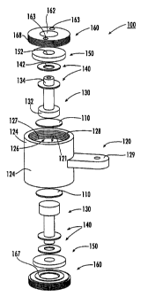
Figure 1 is an exploded, perspective view of a
varistor device according to the present invention;
Figure 2 is a top perspective view of the varistor
device of Figure 1;
Figure 3 is a cross-sectional view of the varistor
device of Figure 1 taken along the line 3-3 of Figure 2;
Figure 4 is a perspective view of a varistor wafer;
Figure 5 is an exploded, perspective view of a
varistor device according to a second embodiment of the
present invention;
Figure 6 is a top perspective view of the varistor
device of Figure 5;
Figure 7 is a bottom perspective view of the
varistor device of Figure 5;
Figure 8 is a view of the varistor device of Figure
5, in which the varistor device is mounted in an
electrical service utility box;
Figure 9 is an exploded, perspective view of a
varistor
CA 02341735 2001-02-26
WO 00/17892 PCT/US99/21899
device according to a third embodiment of the present invention;
Figure 10 is a top, perspective view of the varistor device
of Figure 9; and
Figure 11 is a cross-sectional view of the varistor device
5 of Figure 9 taken along the line 11-11 of Figure 10.
Detailed Description of the Preferred Embodiments
The present invention now will be described more fully
hereinafter with reference to the accompanying drawings, in which
embodiments of the invention are shown. This invention may,
however, be embodied in many different forms and should not be
construed as limited to the embodiments set forth herein; rather,
these embodiments are provided so that this disclosure will be
thorough and complete, and will fully convey the scope of the
invention to those skilled in the art. In the drawings, like
numbers refer to like elements throughout.
With reference to Figures 1-3, an overvoltage protection
device according to a first embodiment of the present invention is
shown therein and designated 100. The device 100 includes a
housing 120 of generally cylindrical shape. The housing is
preferably formed of aluminum. However, any suitable conductive
metal may be used. The housing has a center wall 122 (Figure 3),
cylindrical walls 124 extending from the center wall in opposite
directions, and a housing electrode ear 129 extending outwardly
from the walls 124. The housing is preferably unitary and axially
symmetric as shown. The cylindrical walls 124 and the center wall
122 form cavities 121 on either side of the center wall, each
cavity communicating with a respective opening 126.
A piston-shaped electrode 130 is positioned in each of the
cavities I21. Shafts 134 of the electrodes 130 project outwardly
through the respective openings 126. The electrodes 130 are
preferably formed of aluminum. However, any suitable conductive
metal may be used. Additionally, and as discussed in greater
detail below, a varistor wafer 110, spring washers 140, an
CA 02341735 2001-02-26
WO 00/I7892 PCT/US99/21899
6
insulator ring 150 and an end cap 160 are disposed in each cavity
121.
In use, the device 100 may be connected directly across an AC
or DC input, for example, in an electrical service utility box.
Service lines are connected directly or indirectly to the
electrode shafts 134 and the housing electrode ear 129 such that
an electrical flow path is provided through the electrodes 130,
the varistor wafers 110, the housing center wall 122 and the
housing electrode ear 129. In the absence of an overvoltage
condition, the varistor wafers 110 provide high resistances such
that no current flows through the device 100 as it appears
electrically as an open circuit. In the event of an overvoltage
condition (relative to the design voltage of the device), the
resistances of the varistor wafers decrease rapidly, allowing
IS current to flow through the device 100 and create a shunt path for
current flow to protect other components of an associated
electrical system. The general use and application of overvoltage
protectors such as varistors is well known to those of skill in
the art and, accordingly, will not be further detailed herein.
As will be appreciated from the Figures, the device 100 is
axially symmetric, the upper and lower halves of the device 100
being constructed in the same manner. Accordingly, the device 100
will be described hereinafter with respect to the upper portion
only, it being understood that such description applies equally to
the lower portion.
Turning to the construction of the device 100 in greater
detail, the electrode 130 has a head 132 and an integrally formed
shaft 134. As best seen in Figure 3, the head 132 has a
substantially planar contact surface 132A which faces a
substantially planar contact surface 122A of the housing center
wall 122. The varistor wafer 110 is interposed between the
contact surfaces 122 and 132. As described in more detail below,
the head 132 and the center wall 122 are mechanically loaded
against the varistor wafer 110 to ensure firm and uniform
CA 02341735 2001-02-26
WO 00/17892 PCT/US99/21899
7
engagement between the surfaces 112 and 132A and between the
surfaces 114 and 122A. A threaded bore 136 is formed in the end
of the shaft 134 to receive a bolt for securing a bus bar or other
electrical connector to the electrode 130.
With reference to Figure 4, the varistor wafer 110 has a
first substantially planar contact surface 112 and a second,
opposed, substantially planar contact surface 114. As used
herein, the term "wafer" means a substrate having a thickness
which is relatively small compared to its diameter, length or
width dimensions. The varistor wafer 110 is preferably disk
shaped. However, the varistor wafer may be formed in other
shapes. The thickness T and the diameter D of the varistor 110
will depend on the varistor characteristics desired for the
particular application. Preferably, and as shown, the varistor
wafer 110 includes a wafer 111 of varistor material coated on
either side with a conductive coating 112A, 114A, so that the
exposed surfaces of the coatings 112A and 114A serve as the
contact surfaces 112 and 114. Preferably, the coatings 112A, 114A
are formed of aluminum, copper or solder.
The varistor material may be any suitable material
conventionally used for varistors, namely, a material exhibiting a
nonlinear resistance characteristic with applied voltage.
Preferably, the resistance becomes very low when a prescribed
voltage is exceeded. The varistor material may be a doped metal
oxide or silicon carbide, for example. Suitable metal oxides
include zinc oxide compounds.
The varistor material wafer 111 is preferably formed by first
forming a rod or block(not shown) of the varistor material and
then slicing the wafer 111 from the rod using a diamond cutter or
other suitable device. The rod may be formed by extruding or
casting a rod of the varistor material and thereafter sintering
the rod at high temperature in an oxygenated environment. This
method of forming allows for the formation of a wafer having more
planar surfaces and less warpage or profile fluctuation than would
CA 02341735 2001-02-26
WO 00/17892 PCT/US99/21899
8
typically be obtained using a casting process. The coatings 112A,
114A are preferably formed of aluminum or copper and may be. flame
sprayed onto the opposed sides of the wafer 111.
While the device 100 as shown in Figure 1 includes two spring
washers 140, more or fewer may be used. Each spring washer 140
includes a hole 142 which receives the shaft 134 of the electrode
130. Each spring washer 140 surrounds a portion of the shaft 134
immediately adjacent to the head 132 and abuts the rear face of
the head 132 or the preceding spring washer 140. Each hole 142
preferably has a diameter of between about 0.012 and 0.015 inch
greater than the corresponding diameter of the shaft 134. The
spring washers 140 are preferably formed of a resilient material
and, more preferably, the spring washers 140 are Belleville
washers formed of spring steel.
The insulator ring 150 overlies and abuts the outermost
spring washer 140. The insulator ring I50 has a hole 152 formed
therein which receives the shaft 134. Preferably, the diameter of
the hole 152 is between about 0.005 and 0.007 inch greater than
the corresponding diameter of the shaft 134. The insulator ring
150 is preferably formed of an electrically insulating material
having high melting and combustion temperatures. More preferably,
the insulator ring 150 is formed of polycarbonate, ceramic or a
high temperature polymer.
The end cap 160 overlies and abuts the insulator ring 150.
The end cap 160 has a hole 162 which receives the shaft 134.
Preferably, the diameter of the hole 162 is between about 0.500
and 0.505 inch greater than the corresponding diameter of the
shaft 134 to provide a sufficient clearance gap 165 (Figure 2) to
avoid electrical arcing between the end cap 160 and the electrode
shaft 134 during non-overvoltage conditions. Threads 168 on the
peripheral wall of the end cap 160 engage complementary threads
128 formed in the housing 120. Holes 163 are formed in the end
cap to receive a tool (not shown) for rotating the end cap 160
CA 02341735 2001-02-26
WO 00/17892 PCT/US99/21899
9
with respect to the housing 120. Other means for receiving a
tool, for example, a hex-shaped slot, may be provided in place of
or in addition to the holes 163. The end cap 160 has an annular
ridge 167 which is received within the inner diameter of the
housing 120. The housing 120 includes a rim 127 to prevent
overinsertion of the end cap 150. Preferably, the end cap is
formed of aluminum.
As noted above and as best shown in Figure 3, the electrode
head 132 and the center wall 122 are loaded against the varistor
wafer 110 to ensure firm and uniform engagement between the
surfaces 112 and 132A and between the surfaces 114 and 122A. This
aspect of the device 100 may be appreciated by considering a
method according to the present invention for assembling the
device 100. The varistor wafer 110 is placed in the cavity 121
such that the wafer surface 114 engages the contact surface 122A.
The electrode 130 is inserted into the cavity 121 such that the
contact surface 132A engages the varistor wafer surface 112. The
spring washers 140 are slid down the shaft 134 and placed over the
head 132. The insulator ring 150 is slid down the shaft 134 and
over the outermost spring washer 140. The end cap 160 is slid
down the shaft 134 and screwed into the opening 126 by engaging
the threads 168 with the threads 128 and rotating.
Once the device 100 has been assembled as just described, the
end cap 160 is selectively torqued to force the insulator ring 150
downwardly so that it partially deflects the spring washers 140.
The loading of the end cap 160 onto the insulator ring 150 and
from the insulator ring onto the spring washers 140 is in turn
transferred to the head 132. In this way, the varistor wafer 110
is sandwiched (clamped) between the head 132 and the center wall
122 .
Preferably, the device 100 is designed such that the desired
loading will be achieved when the spring washers 150 are only
partially deflected and, more preferably, when the spring washers
CA 02341735 2001-02-26
WO 00/17892 PCT/US99/21899
are fifty percent (50$) deflected. In this way, variations in
manufacturing tolerances of the other components of the device 100
may be accommodated.
The amount of torque applied to the end cap 160 will depend
5 on the desired amount of load between the varistor wafer 110 and
the head 132 and the center wall 122. Preferably, the amount of
the load of the head and the center wall against the varistor
wafer is at least 264 lbs. More preferably, the load is between
about 528 and 1056 lbs. Preferably, the coatings 112A and 114A
10 have a rough initial profile and the compressive force of the
loading deforms the coatings to provide more continuous
engagements between the coatings and the contact surfaces 122A and
132A.
Alternatively, or additionally, the desired load amount may
be obtained by selecting an appropriate number and or sizes of
spring washers 140. The spring washers each require a prescribed
amount of load to deflect a prescribed amount and the overall load
will be the sum of the spring deflection loads.
Preferably, the area of engagement between the contact
surface 132A and the varistor wafer surface 112 is at least 1.46
square inches. Likewise, the area of engagement between the
contact surface 122A and the varistor wafer surface 114 is
preferably at least 1.46 square inches. Preferably, the electrode
head 132 has a thickness H of at least 0.50 inch. The center wall
122 preferably has a thickness W of at least 0.25 inch.
The combined thermal mass of the housing 120 and the
electrode 130 should be substantially greater than the thermal
mass of the varistor wafer 110. As used herein, the term "thermal
mass" means the product of the specific heat of the material or
materials of the object (e. g., the varistor wafer 110) multiplied
by the mass or masses of the material or materials of the object.
That is, the thermal mass is the quantity of energy required to
raise one gram of the material or materials of the object by one
degree centigrade times the mass or masses of the material or
CA 02341735 2001-02-26
WO 00/17892 PCT/US99/21899
11
materials in the object. Preferably, the thermal masses of each
of the electrode head 132 and the center wall 122 are
substantially greater than the thermal mass of the varistor wafer
110. Preferably, the thermal masses of each of the electrode head
132 and the center wall 122 are at least two (2) times the thermal
mass of the varistor wafer 110, and, more preferably, at least ten
(10) times as great.
The overvoltage protection device 100 provides a number of
advantages for safely, durably and consistently handling extreme
and repeated overvoltage conditions. The relatively large thermal
masses of the housing 120 and the electrode 130 serve to absorb a
relatively large amount of heat from the varistor wafer 110,
thereby reducing heat induced destruction or degradation of the
varistor wafer as well as reducing any tendency for the varistor
wafer to produce sparks or flame. The relatively large thermal
masses and the substantial contact areas between the electrode and
the housing and the varistor wafer provide a more uniform
temperature distribution in the varistor wafer, thereby minimizing
hot spots and resultant localized depletion of the varistor
material.
The loading of the electrode and the housing against the
varistor wafer as well as the relatively large contact areas
provide a more even current distribution through the varistor
wafer 10. As a result, the device 100 responds to overvoltage
conditions more efficiently and predictably, and high current
spots which may cause pinholing are more likely to be avoided.
The tendency for the varistor wafer 110 to warp responsive to high
current impulses is reduced by the mechanical reinforcement
provided by the loaded head 132 and center wall 122. The spring
washers may temporarily deflect when the varistor wafer expands
and return when the varistor wafer again contracts, thereby
maintaining the load throughout and between multiple overvoltage
events. Moreover, during an overvoltaqe event, the device 100
will generally provide lower inductance and lower resistance
CA 02341735 2001-02-26
WO 00/17892 PCT/US99/21899
12
because of the more uniform and efficient current distribution
through the varistor wafer.
The device 100 also serves to prevent or minimize the
expulsion of flame, sparks and/or varistor material upon
overvoltage failure of the varistor wafer 110. The strength of
the metal housing as well as the configuration of the electrode
130, the insulator ring 150 and the end cap 160 serve to contain
the products of a varistor wafer failure. In the event that the
varistor destruction is so severe as to force the electrode 130
away from the varistor and melt the insulator ring 150, the
electrode 130 will be displaced into direct contact with the end
cap 160, thereby shorting the electrode 130 and the housing 120
and causing an in-line fuse (not shown) to blow.
While the housing 120 is illustrated as cylindrically shaped,
the housing may be shaped differently. The lower half of the
device 100 may be deleted, so that the device 100 includes only an
upper housing wall 124 and a single varistor wafer, electrode,
spring washer or set of spring washers, insulator ring and end
cap.
Methods for forming the several components of the device will
be apparent to those of skill in the art in view of the foregoing
description. For example, the housing 120, the electrode 130, and
the end cap 160 may be formed by machining, casting or impact
molding. Each of these elements may be unitarily formed or formed
of multiple components fixedly joined, by welding, for example.
With reference to Figures 5-8, a varistor device 200
according to a second embodiment of the present invention is shown
therein. The varistor device 200 includes elements 210, 230, 240
and 260 corresponding to elements 110, 130, 140 and 160,
respectively, of the varistor device 100. The varistor device 200
differs from the varistor device 100 in that the device 200
includes only a single varistor wafer 210 and corresponding
components. The varistor device 200 includes a housing 220 which
is the same as the housing 120 except as follows. The housing 220
CA 02341735 2001-02-26
WO 00/17892 PCT/US99/21899
13
defines only a single cavity 221, and has only a single
surrounding wall 224 extending from the center (or end) wall. 222
thereof. Also, the housing 220 has a threaded stud 229 (Figure 7)
extending from the lower surface of the center (or end) wall 222
rather than a sidewardly extending electrode ear corresponding to
the electrode ear 129. The stud 229 is adapted to engage a
threaded bore of a conventional electrical service utility box or
the like.
The varistor device 200 further differs from the varistor
device 100 in the provision of an insulator ring 251. The
insulator ring 251 has a main body ring 252 corresponding to the
insulator ring 150. The ring 251 further includes a collar 254
extending upwardly from the main body ring 252. The inner
diameter of the collar 254 is sized to receive the shaft 234 of
the electrode 230, preferably in clearance fit. The outer
diameter of the collar 254 is sized to pass through the hole 262
of the end cap 260 with a prescribed clearance gap 265 (Figure 6)
surrounding the collar 254. The gap 265 allows clearance for
inserting the shaft 134 and may be omitted. The main body ring
252 and the collar 254 are preferably formed of the same material
as the insulator ring 150. The main body ring 252 and the collar
254 may be bonded or integrally molded.
With reference to Figure 8, the varistor device 200 is shown
therein mounted in an electrical service utility box 10. The
varistor device 200 is mounted on a metal platform 12 electrically
connected to earth ground. The electrode stud 229 engages and
extends through a threaded bore 12A in the platform 12. A bus bar
16, electrically connected a first end of a fuse 14, is secured to
the electrode shaft 234 by a threaded bolt 18 inserted into the
threaded bore 236 of the electrode 230. A second end of the fuse
may be connected to an electrical service line or the like. As
shown in Figure 8, a plurality of varistor devices 200 may be
connected in parallel in a utility box 10.
CA 02341735 2001-02-26
WO 00/17892 PCT/US99/21899
14
With reference to Figures 9-11, a varistor device 300
according to a third embodiment of the present invention is .shown
therein. The varistor device 300 includes elements 310, 330, 340
and 351 corresponding to elements 210, 230, 240 and 251,
respectively. The varistor device 300 also includes a flat metal
washer 345 interposed between the uppermost spring washer 340 and
the insulator ring 351, the shaft 334 extending through a hole 346
formed in the washer 345. The washer 345, which may be
incorporated into the devices 100, 200, serves to distribute the
mechanical load of the uppermost spring washer 340 to prevent the
spring washer from cutting into the insulator ring 351. The
housing 320 is the same as the housing 220 except as follows.
The housing 320 of device 300 does not have a rim
corresponding to the rim 127 or threads corresponding to the
IS threads 128. Also, the housing 320 has an internal annular slot
323 formed in the surrounding sidewall 324 and extending adjacent
the opening 326 thereof.
The varistor device 300 also differs from the varistor
devices 100, 200 in the manner in which the electrode 330 and the
center wall 322 are loaded against the varistor wafer 310. In
place of the end caps 160, 260, the varistor device 300 has an end
cap 360 and a resilient clip 370. The clip 370 is partly received
in the slot 323 and partly extends radially inwardly from the
inner wall of the housing 320 to limit outward displacement of the
end cap 360. The clip 370 is preferably formed of spring steel.
The end cap 360 is preferably formed of aluminum.
The varistor device 300 may be assembled in the same manner
as the varistor devices 100, 200 except as follows. The end cap
360 is placed over the shaft 334 and the collar 354, each of which
are received in a hole 362. The washer 345 is placed over the
shaft 334 prior to placing the insulator ring 351. A jig (not
shown) or other suitable device is used to force the end cap 360
down, in turn deflecting the spring washers 340. While the end
CA 02341735 2001-02-26
WO 00/17892 PCT/US99/21899
cap 360 is still under the load of the jig, the clip 370 is
compressed, preferably by engaging apertures 372 with pliers, or
another suitable tool, and inserted into the slot 323. The clip
370 is then released and allowed to return to its original
5 diameter, whereupon it partly fills the slot and partly extends
radially inward into the cavity 321 from the slot 323. The clip
370 and the slot 323 thereby serve to maintain the load on the end
cap 360.
Means other than those described above may be used to load
10 the electrode and housing against the varistor wafer. For
example, the electrode and end cap may be assembled and loaded,
and thereafter secured in place using a staked joint.
In each of the aforedescribed devices 100, 200, 300, multiple
varistor wafers (not shown) may be stacked and sandwiched between
15 the electrode head and the center wall. The outer surfaces of the
uppermost and lowermost varistor wafers would serve as the wafer
contact surfaces. However, the properties of the varistor wafer
are preferably modified by changing the thickness of a single
varistor wafer rather than stacking a plurality of varistor
wafers .
As discussed above, the spring washers 140 are preferably
Belleville washers. Belleville washers may be used to apply
relatively high loading without requiring substantial axial space.
However, other types of biasing means may be used in addition to
or in place of the Belleville washer or washers. Suitable.
alternative biasing means include one or more coil springs, wave
washers or spiral washers.
The foregoing is illustrative of the present invention and
is not to be construed as limiting thereof. Although a few
exemplary embodiments of this invention have been described,
those skilled in the art will readily appreciate that many
modifications are possible in the exemplary embodiments without
materially departing from the novel teachings and advantages of
this invention. Accordingly, all such modifications are intended
CA 02341735 2001-02-26
WO 00/17892 PCT/US99/21899
16
to be included within the scope of this invention as defined in
the Claims. In the Claims, means-plus-function clauses axe
intended to cover the structures described herein as performing
the recited function and not only structural equivalents but also
equivalent structures. Therefore, it is to be understood that
the foregoing is illustrative of the present invention and is not
to be construed as limited to the specific embodiments disclosed,
and that modifications to the disclosed embodiments, as well as
other embodiments, are intended to be included within the scope
of the appended Claims. The invention is defined by the
following Claims, with equivalents of the Claims to be included
therein.