Note: Descriptions are shown in the official language in which they were submitted.
CA 02341817 2001-03-22
FIELD OF THE INVENTION
This invention relates to a method and apparatus for the generation and
control of spin currents, comprising spin polarized charge carriers, in
photoconductors. More particularly the present invention provides a method of
using the polarization properties of multiple coherent light beams, and phase
differences between multiple coherent light beams, to control the magnitude
and
direction of spin currents in a photoconductor.
BACKGROUND OF THE INVENTION
The control of electronic spin in semiconductors is important for the study
of spin dynamics in many-body systems and crucial for the development of new
data storage and processing methods based on the spin degree of freedom of
charged particles. This will be essential as a first step towards a solid
state
implementation of a quantum computer; see, e.g. D. D. Awschalom and J.M.
Kikkawa, Phys. Today 52, No. 6, 33 (1999).
There has been considerable work on achieving spin-polarized currents in
semiconductors using transport in the presence of magnetic impurities, see M.
Oestreich et al. Appl. Phys. Lett. 74, 1251 (1999), R. Fiederling et al.,
Nature
(London) 402, 787, (1999) and Y. Ohno et al., Nature (London) 402, 790,
(1999),
or using injection of carriers from a ferromagnetic contact, see P.R. Hammar
et
al., Phys. Rev. Lett. 83, 203 (1999), and S. Gardelis et al., Phys. Rev. B 60,
7764
(1999). In these cases a voltage applied across the semiconductor drives the
spin current.
CA 02341817 2001-03-22
It is known that spin-polarized carriers can be optically injected into a
semiconductor using circularly polarized light, see United States Patent No.
3,968,376, and M. I. Dyakonov and V.I. Perel, in Optical Orientation, edited
by F.
Meier and B. P. Zakharchenya, Modern Problems in Condensed Matter
Sciences, Vol. 8 (North-Holland, Amsterdam, 1984), Chapter 2. A spin current
may be generated from these spin-polarized carriers by applying a voltage
across the semiconductor, see D. Hagele et al., Appl. Phys. Lett. 73, 1580
(1980), and J.M. Kikkawa and D. D. Awschalom, Nature (London) 397, 139
(1999).
All of the above methods use a voltage difference to move the carriers
(electrons and holes), and hence there is always an electrical current as well
as a
spin current. As well, the spin currents can only be modulated as fast as the
voltage difference can be modulated.
United States Patent No. 5,790,296 discloses a method for generating and
controlling an electrical current in a semiconductor using the interference
between multiple laser beams. This patent is restricted to the ways in which
multiple light beams can be used to generate and control electrical currents,
and
does not discuss how to generate and control spin-polarized currents.
It would therefore be very advantageous to provide a method of
generating polarized spin currents in photoconductors that can be modulated on
ultrafast timescales without the need for a bias voltage to be applied.
2
CA 02341817 2001-03-22
SUMMARY OF THE INVENTION
The present invention provides a method of generating in photoconductors
polarized spin currents that can be modulated on ultrafast timescales without
the
need for a bias voltage to be applied.
S As used herein, the term spin current means a current of charges (such as
electrons and holes) which are spin polarized. The method utilizes the quantum
interference of one-and two-photon absorption processes in a light field
produced
preferably by multiple laser beams. Spin currents can be produced with or
without accompanying net electrical currents depending on the polarization of
the
beams with respect to each other. The magnitude and direction of the spin
currents are determined by the phase difference between multiple laser beams,
and the polarization of the beams.
In one aspect of the invention there is provided a method of generating
spin currents in a photoconductor material, the method comprising the steps
of:
producing a first coherent light beam having a first frequency c~~ and a
second coherent light beam having a frequency twice the first frequency 2c~~,
polarizing said first and second coherent light beams to have a preselected
polarization with respect to each other, and simultaneously irradiating a
selected
region of the photoconductor material with said first coherent light beam and
said
second coherent light beam to generate a spin current in said photoconductor.
The present invention is not restricted to a requirement for two coherent
light beams. Thus, in anther aspect fo the invention there is provided a
method of
3
CA 02341817 2001-03-22
generating spin currents in a photoconductor material, the method comprising
the
steps of:
producing at least three coherent light beams of frequencies c~~, w2, and
w3, such that UJ~=OJ2~'GJ3, polarizing each of said at least three coherent
light
beams to have a preselected polarization with respect to the other coherent
light
beams, and simultaneously irradiating a selected region of the photoconductor
material with said at least three coherent light beams to generate a spin
current
in said photoconductor.
In the above aspects of the invention the method may include adjusting a
phase relationship between the coherent light beams to change the direction of
the spin current generated in the photoconductor.
While using multiple laser beams is a preferred embodiment, the method
of the present invention may also be achieved using single optical pulses that
contain within the pulses the multiple frequency components required to give
the
1 S same effect achieved using multiple laser beams.
BRIEF DESCRIPTION OF THE DRAWINGS
Preferred embodiments of the invention will now be described, by way of
example only, with reference to the drawings, in which:
Figure 1 shows a block diagram of an apparatus used to produce spin
currents using two coherent light beams in accordance with the present
invention;
4
CA 02341817 2001-03-22
Figure 2 shows an alternative embodiment of an apparatus used to
produce spin currents using two coherent light beams; and
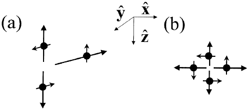
Figure 3 shows schematic illustrations of the net electron motion for (a)
the case with both beams right circularly polarized using the apparatus of
Figure
2, and (b) the case with the coherent light beams cross-polarized.
DETAILED DESCRIPTION OF THE INVENTION
The spin current is denoted by the second rank pseudotensor Kab=<Sa~'>
where <Sa~'> denotes the average of the product of carrier spin and velocity,
the
vector S is the carrier spin, and the vector v is the carrier velocity.
Superscript
letters denote Cartesian components of vectors or tensors, and can take on one
of the values x, y, or z. Without limiting the invention, we expect the spin
current
satisfies
K ab = ~ abcde (E(o ~ ~ ~, ~~2 Ew 3 + C.C. ~ K ab /T ~1~
IS
where E~,~, E~,2, and Ew3 are the (complex) field vector amplitudes of the
beams,
K
is the time rate of change of the spin current pseudotensor, ~ is a fifth rank
material response pseudotensor, and T is a phenomenological relaxation time.
For materials with cubic or isotropic symmetry, ~ can be written in terms of
only
four parameters C~_4 as
abcde = C,f ~ ad ~ bce + ~ ae~ bcd ~ C,Z ~ bd E ace + b 6e~ acd ~ C,3S deE abc
+ C4 ~ cd E abe + ~ ceE abd
5
CA 02341817 2001-03-22
where 8ab IS a Kronecker delta, and sabc is the Levi-Cevita tensor.
There are two cases of interest for these materials. We will assume the beams
are co-propagating along the z-axis. The first case is where the beams
cocircularly polarized all having the same circular polarization. In this
case, there
is a net current from the interference of the beams as described in United
States
Patent No. 5,790,296. The electrical current is in the plane perpendicular to
the
beam propagation direction, and its direction in that plane depends on the
relative phase of the beams. Calling that direction m, we have
m = x sin~0~ ~~ y cos~0~
where the top sign is for right-circularly polarized beams and the bottom sign
is
for left-circularly polarized beams, and
~~ -'Yw2 +'1'm3 ~wl
The optically injected carriers have a net spin along the axis of
propagation of the coherent light beams, thus the current is spin polarized.
Even
though the carriers should only be 50% spin polarized, the current can have a
higher degree of spin polarization: 57% for GaAs, see R.D.R. Bhat and J.E.
Sipe
Phys. Rev. Lett. 85, 5432 (2000). There will also be a spin current such that
the
spin component along m of carriers with a component of motion along positive z
will be opposite to the spin component along m of carriers with a component of
motion along negative z. This is a pure spin current, since there is no
electrical
6
CA 02341817 2001-03-22
current along the z direction. Figure 3(a) shows a schematic illustration of
the net
electron motion for with both beams right circularly polarized using the
apparatus
of Figure 2 discussed hereinafter.
The second case of interest is when the beams have crossed linear
polarization, such that for example, the c~~ beam is polarized along y, while
the
other two beams are polarized along x. In this case, there is no net spin
polarization of the carriers, but there are spin currents nonetheless. The
electrical
current as described in United States Patent No. 5,790,296 (which is
incorporated herein in its entirety) is in the direction of the polarization
of the c~,
beam and its magnitude depends sinusoidally on ~~. In the present invention
there are pure spin currents perpendicular to the electrical current. Carriers
with
a component of motion along positive x will have their spin along z opposite
to
carriers with a component of motion along negative x. Also carriers with a
component of motion along positive z will have their spin along x opposite to
carriers with a component of motion along negative z. Both of these pure spin
currents will have a magnitude which depends on the cosine of o~. Figure 3(b)
shows a schematic illustration of the net electron motion obtained with the
cross-
polarized coherent light beams using the apparatus of Figure 1 discussed
hereinafter.
The two cases described above for cubic or isotropic materials are
illustrative important examples. In general the beams need not be co-
propagating, and other polarization combinations may be used. Further, the
method disclosed herein for producing spin currents does not rely on any
specific
7
CA 02341817 2001-03-22
crystal symmetry so that materials of different symmetry could be used. In the
general case, the spin current is contemplated by the inventors to still be
well
described by equation (1 ). Further, it is contemplated that spin currents can
be
produced in materials having nanostructure geometries using the method
disclosed herein.
Even more generally, one could replace any one of the beams by one or
more beams of lower frequency but higher intensity such that the role of
each photon from the original beam is taken on by an odd number of
photons from the new beams. For example, a beam of frequency c~2 may be
replaced by two beams of frequencies G)A=c~2/3 and wB=2w2/3, so that the role
of
each photon of frequency w2 is replaced by two photons of frequency c~A and
one
of frequency wB.
An apparatus 10 for producing spin current in a two color field using two
coherent light beams of frequency c~9 and 2~g is shown in Figure 1. A light
source 12 produces a coherent light beam 14, such as a laser beam. An example
source 12 may be an actively mode locked picosecond Ti:sapphire laser
operating at 800 nm with a corresponding frequency w9. The first beam wg pumps
an optical parametric generator 16. A lens L1 having a focal length of f=5 cm
focuses the light beam wg passing through the chopper 20 onto a 1 mm thick ~3-
barium borate (BBO) crystal 30 using type I phase matching which generates a
second beam (hereinafter 2wg) as the second harmonic of the first beam w9.
The two beams w9 and 2w9 are focused by curved mirror MC1 to the flat
mirror MF3, which directs the two beams to the planar dichroic mirror D set at
an
8
CA 02341817 2001-03-22
angle of 45 degrees with respect to the direction of the beams. The wg beam is
transmitted by dichroic plate D, whereupon it is back-reflected by flat mirror
MF4
that can be translated by a piezoelectric transducer (PZT) to control the
relative
phase of the two beams. The 2wg beam is simply reflected by D and then back-
s reflected by flat mirror MFS. The two beams are reflected off (2wg), and
transmitted through (w9), dichroic mirror D towards planar mirror MC2 which
reflects both beams onto curved mirror MC2 which in turn focuses both beams
onto a selected area on photoconductor 26. The two beams, after being back-
reflected from MF5 and MF4 off, and through D, will have crossed linear
polarizations with respect to each other.
The two cross-polarized beams wg and 2wg are focused onto the surface
close to one side of the photoconductor 26, and a polarizer 32 is placed in
front
of the photoconductor 26 to analyze the polarization of the luminescence
emitted
from the photoconductor. The luminescence is collected by a photodetector 34
that is connected to the lock-in amplifier 22. Apparatus 10 includes a chopper
20
connected to a lock-in amplifier 22. In combination the chopper 20 and lock-in
amplifier 22 average the signals produced by the coherent light beams.
Detection
of the polarization of the luminescence will in effect measure the spin
current
because the carriers scattering off the edge 27 of the photoconductor 26 will
have their spins randomized. Those spin-polarized carriers moving in the
opposite direction in photoconductor 26 away from edge 27 will not have their
spins randomized as quickly, and thus if the spins moving in the opposite
direction have opposite spins, the result will be a net spin polarization of
the
9
CA 02341817 2001-03-22
carriers that will be seen through the degree of circular polarization of the
luminescence emitted from the photoconductor.
Other polarization combinations can also be realized. For example,
referring to Figure 2, co-circularly polarized beams are produced by modifying
the apparatus of Figure 1 to give apparatus 40 by the addition of a 7~/8
waveplate
42 into the optical circuit between dichroic mirror D and mirror MF4 through
which the w9 beam is transmitted twice and a ~,/8 waveplate 44 between
dichroic
mirror D and mirror MF5 through which the 2w9 beam is transmitted twice.
The embodiments of the apparatus shown in Figures 1 and 2 for
producing spin currents used only two beams, such that one has twice the
frequency of the other. However, the method of producing spin currents in
accordance with the present invention may be implemented in general with three
beams of frequencies c~~, c~2, and c~3, such that Co~=G)2+w3. The magnitude of
the
frequencies should be such that the beam with largest frequency has a photon
energy that is large enough to excite carriers across the bandgap of the
photoconductor. If the photon energy is too large such that it can excite
carriers
from the spin-orbit split-off band, the magnitude of the effect will be
decreased.
While using multiple coherent light beams such as laser beams is a
preferred embodiment, the method of the present invention may also be
achieved using single optical pulses short enough to give the required
bandwidth
that contain within the pulses the multiple frequency components required to
give
the same effect achieved using multiple laser beams.
CA 02341817 2001-03-22
The foregoing description of the preferred embodiments of the invention
has been presented to illustrate the principles of the invention and not to
limit the
invention to the particular embodiment illustrated. It is intended that the
scope of
the invention be defined by all of the embodiments encompassed within the
following claims and their equivalents.