Note: Descriptions are shown in the official language in which they were submitted.
CA 02341847 2001-03-22
-1-
METHOD AND SYSTEM FOR CARRIER RECOVERY
FIELD OF THE INVENTION
The present invention relates to a method and system for achieving carrier
frequency
synchronization in a high speed receiver. In particular, the present invention
relates to the
carrier recovery loop in a high-speed digital demodulator that compensates for
the phase and
frequency offsets that are present in the complex baseband signal recovered
from the
receiver.
BACKGROUND OF THE INVENTION
In modern digital receivers, the digital complex baseband signal recovered
from the
analog-to-digital converter invariably contains residual carrier frequency
errors due to
mismatches between the transmit and receive local oscillators. These residual
carrier errors
must be removed before the baseband signal can be further processed and
outputted. One
system for correcting this residual carrier error uses a carrier recovery loop
circuit that
provides compensating feedback phase and frequency offsets to the corrupted
complex
baseband signal. Fig. 1 illustrates the interconnectivity of such a earner
recovery loop 20
between an equalizer 22 and an air interface processor 24, and a earner
recovery (CR)
subsystem 25.
As further shown in Fig. 2, a typical CR loop 20 consists of the following
components: a phase derotator 26, a dicer 27, and the CR subsystem 25
consisting of a phase
error detector 28, a loop filter 30, a earner acquisition control 32, a phase
accumulator and
sine and cosine look-up table (LUT) 34, and a CR lock detector 36. In
operation, the CR loop
20 remains inactive following power-up until the air interface processor (AIP)
24 in Fig. 1
gives a carrier-synchronization-enable signal. The earner loop 20 works in
collaboration with
the equalizer 22. The AIP 24 activates the CR loop 20 once the equalizer
Constant Modulus
Algorithm (CMA) mode has converged sufficiently. It is assumed that the
frequency offset
encountered by the CR loop 20 is in the order of ~5% of the highest symbol
rate of the
digital demodulator. The earner loop 20 can operate at a rate of one sample
per symbol or at
a reduced rate as programmed by the air interface processor 24. In lower data
rate
applications where the equalizer 22 is not required, the equalizer taps are
bypassed. However,
CA 02341847 2001-03-22
-2-
the dicer 27 will still continue to feed the quantized decisions ( q" ) to CR
loop 20. Typically,
the input ( y" ) to the slicer 27 has a word length of 12-bits and the output
( q" ) is 3-bits wide.
Both y" and q" feed the CR sub-system 25.
When the initial frequency offset encountered by the earner recovery loop 20
is in the
order of ~ 5% of the symbol rate, the CR loop 20 cannot always lock on to, and
compensate
for, the incoming offset frequency in an unaided fashion. Therefore, the
following acquisition
technique has been used in prior art sytems to achieve better earner lock. The
frequency of
the VCO is swept linearly across the range spanning the maximum frequency
offset
encountered by the receiver. This is done by feeding a linearly changing dc-
voltage to the
output of the loop filter of Fig. 2 prior to the phase accumulator 34. When
the VCO
frequency and the residual offset frequency at the phase derotator 26 input
coincide, the
earner loop 20 will lock, and the lock detector 36 indicates to the
acquisition control unit 32
to freeze the do sweep value. The CR loop 20 enters tracking mode at this
point. Fig. 3
illustrates the earner acquisition process of a typical carrier recovery loop
sub-system.
In a high-speed receiver system, hardware realization of the multipliers and
adders
used in the CR sub-system 25 can produce pipeline delays that are based on the
number of
hardware clock cycles available for performing computations. Given a maximum
operating
clock frequency of the system, there are a limited number of hardware clock
cycles between
consecutive data samples at the higher data rates. For instance, at data rates
of 155 Mbits per
second, the maximum clock frequency becomes close or equal to the typical data
sampling-
rate. Each hardware multiplication and addition operation in the earner
recovery feedback
loop 20 will therefore introduce pipeline delays. The presence of such delays
in the feedback
loop 20 introduces instabilities in the carrier acquisition scheme due to the
addition of
unwanted poles in the closed loop system response. When there is an excessive
number of
delays present in the feedback loop, the carrier loop 20 is not able to
achieve carrier lock even
with an aided acquisition scheme.
It is, therefore, desirable to provide a method and system for alleviating the
adverse
effects of pipeline delays in a earner recovery loop.
CA 02341847 2001-03-22
-3-
SUMMARY OF THE INVENTION
It is an object of the present invention to obviate or mitigate at least one
disadvantage
of previous systems and methods for earner recovery in digital communication
systems.
In a first aspect, the present invention provides a frequency compensation
method for
a carrier recovery system in a digital demodulator. The method consists of
reducing a
sampling rate, from a symbol rate to a down-sampled rate, of signals by a down-
sampling
factor. The signals are received at a phase error detector from a phase
derotator and a dicer.
When a earner lock condition is detected at the down-sampled rate, the outputs
of a phase
accumulator are determined. Extrapolated outputs, between successive
determined outputs,
can then be extrapolated to generate addresses to a symbol rate look-up table.
Compensating
frequency and phase compensation offsets, for input to the phase derotator,
can then be
looked up at the generated addresses.
In a presently preferred embodiment, the down-sampling factor is determined
such
that a predetermined maximum allowable pipeline delay is not exceeded. The
down-sampling
factor can be derived from the symbol rate and the channel condition. The
extrapolated
outputs are determined by calculating a gradient of the phase accumulator
outputs. The
address generation is accomplished by combining the phase accumulator outputs
and the
extrapolated outputs, and reformatting the combined phase accumulator outputs
and
extrapolated outputs.
In a further aspect, the present invention provides a carrier recovery system
for a
digital receiver. The carrier recovery system includes a phase derotator for
derotating a signal
received from an equalizer, a slicer, communicating with the phase derotator,
for providing a
quantized decision of the signal, and a feedback loop. The feedback loop has
down-sampling
means that reduce the sampling rate of signals from the phase derotator and
the slicer by a
down-sampling factor, from a symbol rate to a down-sampled rate. A phase error
detector
detects phase errors at the down-sampled rate, feeds the detected errors to a
loop filter, a
earner acquisition control and carrier recovery lock, which then determine a
carrier lock
condition. A phase accumulator then provides outputs at the down-sampled rate,
which are
used by a look-up table address generation unit to extrapolate extrapolated
outputs between
the phase accumulator outputs to provide look-up table addresses at the symbol
rate. A
symbol rate look-up table is then used to generate, by reference to the look-
up table
CA 02341847 2001-03-22
-4-
addresses, compensating frequency and phase compensation offsets for input to
the phase
derotator.
In a presently preferred embodiment, the down-sampling means includes means
for
determining the down-sampling factor such that a predetermined maximum
allowable
S pipeline delay is not exceeded, based on the symbol rate and data channel
condition. The
look-up table address generation unit includes a gradient computation unit for
determining a
gradient of the outputs of the phase accumulator, for combining the outputs of
the phase
accumualator and the extrapolated outputs, and reformatting the combined phase
accumulator
outputs and extrapolated outputs to provide the look-up table addresses. The
look-up table
address generation unit includes a multiplexer unit for providing the look-up
table addresses
to the symbol rate look-up table.
Other aspects and features of the present invention will become apparent to
those
ordinarily skilled in the art upon review of the following description of
specific embodiments
of the invention in conjunction with the accompanying figures.
BRIEF DESCRIPTION OF THE DRAWINGS
Embodiments of the present invention will now be described, by way of example
only, with reference to the attached Figures, wherein:
Figure 1 is a block diagram showing the prior art interconnection between an
equalizer, an air interface processor and a carrier recovery system;
Figure 2 is a block diagram of a prior art carrier recovery system;
Figure 3 is a flow chart showing the earner acquisition process in a prior art
carrier
recovery system;
Figure 4 is a block diagram of a earner recovery system according to the
present
invention;
Figure 5 is a block diagram of a look-up table address generation unit
according to the
present invention;
Figure 6 is a diagram showing a phase accumulator gradient calculation unit
according to the present invention;
Figure 7 is a diagram showing a multiplexing according to the present
invention; and
CA 02341847 2001-03-22
- 5 -
Figure 8 is a diagram of exemplary phase accumulator outputs and extrapolated
points
according to the present invention.
DETAILED DESCRIPTION
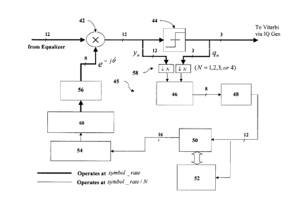
Referring to Fig. 4, a Garner recovery system 40 according to the present
invention is
shown. The carrier recovery loop forms part of a high data rate digital
demodulator, or digital
receiver, and compensates for carrier frequency errors due to mismatches
between transmit
and receive local oscillators. Typically, the carrier recovery loop 40
operates in conjunction
with an equalizer (not shown), from which it receives a filtered signal. The
resulting
compensated signal is provided to timing recovery and IQ generator modules
(not shown) for
further processing.
The Garner recovery system 40 consists of a phase derotator 42, a slicer 44,
and a
feedback loop 45 having a phase error detector 46, a loop filter 48, a Garner
acquisition
control 50 communicating with a Garner recovery lock detector 52, a phase
accumulator 54,
and a sine cosine look-up table 56, as in previously known carrier recovery
loops. In addition,
the Garner recovery loop 40 includes down-sampling means 58, and a symbol rate
address
generation unit 60, the operation of which will be described below.
Generally, the present invention provides a method and system for alleviating
the
adverse effects of pipeline delays on the carrier recovery system 40 in high
data rate systems.
The present invention employs a combination of reduced sampling rate at the
phase error
detector 46 and an extrapolation method for reconstructing the sampling rate
to the original
symbol rate at the look-up tables) 56. Hardware realization of the multipliers
and adders in a
conventional Garner recovery system result in pipeline delays that are based
on the number of
hardware clock cycles available for performing computations. Given the maximum
operating
clock frequency of the system, there are a limited number of hardware clock
cycles between
consecutive data samples at the higher data rates. for example, at data rates
of 155 Mbits per
second, the maximum clock frequency becomes close or equal to the data
sampling-rate.
Each multiply and add operation in the carrier recovery feedback loop will
therefore,
introduce pipeline delays. The presence of pipeline delays in the feedback
loop introduces
instability by the addition of unwanted poles in the closed loop system
response. When there
is an excessive number of delays present in the feedback loop, the carrier
recovery system 40
CA 02341847 2001-03-22
-6-
will not be able to achieve carrier lock even with an aided acquisition
scheme. For receivers
operating at lower incoming data rates, reduced sampling is not necessary
because more
hardware clock cycles are available for computations between samples,
therefore the Garner
loop does not need to be run at a reduced rate.
This method of the present invention is accomplished as follows: The input to
the
phase error detector 46 is down-sampled by a factor of N (N=l, 2, 3, 4...) by
the down-
sampling means 58. This causes the feedback loop of the carrier recovery
system 40 to run at
a lower, down-sampled rate of symbol _ rate l N . At this lower operating
rate, more hardware
clock cycles are available for computations between successive samples within
the feedback
loop of the Garner recovery system 40. The net effect is that the pipeline
delays seen by the
phase derotator 42 and slicer 44 will be reduced. The feedback loop of the
carrier recovery
system 40 is operated at the reduced rate until carrier lock is achieved.
Using combined
down-sampling and acquisition control techniques, it is possible to handle up
to a
predetermined maximum number of pipeline delays in the carrier recovery system
40. Based
on the highest operating clock frequency, the selection of down-sampling
factor in a presently
preferred embodiment is based on the symbol transmission rate, or symbol rate,
and channel
condition such that the total number of pipeline delays seen by the feedback
loop does not
exceed the maximum allowable delay. The down-sampled rate at which the
feedback loop of
the Garner recovery system 40 operates is programmed by an air interface
processor (not
shown) that controls Garner recovery in the digital receiver, and to which the
carrier lock
condition is communicated.
While reducing the symbol rate to the down-sampled rate alleviates the
pipeline delay
in the carrier recovery system 40, it creates another problem in closing the
recovery loop.
Since the phase derotator 42 and dicer 44 must always operate at the symbol
rate, it is
necessary that the down-sampled rate be reconverted to the original symbol
rate before
passing to the look-up table 56. This reconversion is performed by an
extrapolation technique
between the phase accumulator 54 and the look-up table 56 that regenerates the
Garner
phase/frequency correction offsets for the phase derotator 42 at the original
symbol rate. The
symbol rate address generation unit 60, at the output of the phase accumulator
54 reconstructs
the reduced sample rate to the original symbol rate at the look-up table 56.
CA 02341847 2001-03-22
-
The down-sampled earner feedback loop is run until the carrier acquisition
control 50
and the lock detector 52 determine that earner lock has been achieved. At this
point, the
phase accumulator output displays a constant slope that is proportional to the
carrier offset
encountered by the loop. To restore the original symbol rate, the current
value of the phase
accumulator output is extrapolated in order to generate N 1 more addresses for
the look-up
table 56 between consecutive output samples from the phase accumulator. This
procedure is
shown in greater detail in Figs. 5, 6, and 7.
Referring to Fig. 5, the address generation unit 60 is shown in greater
detail. A phase
accumulator output gradient computation unit 70 operates at symbol _ rate l N
, where N=4.
Once a slope value has been computed, the additional N 1 phase accumulator
outputs are
obtained by adding the offset values to the current phase accumulator output,
as shown. The
N phase accumulator outputs are reformatted to generate N look-up table
addresses. These N
look-up table addresses are then selected consecutively by a multiplexer (Mux)
unit 72 to
address the look-up table 56. The Mux unit select signal operates at the
symbol rate. Figs. 6
and 7 show presently preferred functional configurations for the phase
accumulator gradient
computation unit 70 and Mux unit 72, respectively.
Referring to Fig. 8, an example phase accumulator output once earner lock has
been
achieved is shown. In the example, a down-sampling factor of N=4 is used. The
phase
accumulator outputs at the down-sampled rate are referenced at 80. The
expected phase
accumulator output is a quantized sawtooth, as shown by the dashed line 82.
Therefore, the
gradient, or slope, between the down-sampled outputs can be determined, as
shown in Fig. 6,
and a linear extrapolation based on the determined slope can be used to
extrapolate the N 1
extrapolated outputs 84 (i.e. three in the example shown). The combination of
the actual
phase accumulator outputs 80, at the down-sampled rate, and the extrapolated
outputs 84
provide an extrapolated phase accumulator output at the original symbol rate
used to generate
addresses for input to the look-up table.
In summary, for high data rate receivers, the present invention provides a
combination
of down-sampling and extrapolation methods to operate the feedback loop in a
carrier
recovery system 40 at a reduced rate, while operating its phase derotator 42
and dicer 44 at
the symbol rate. The total pipeline delay as seen by the earner recovery
system is thus
reduced. This in turn allows for more efficient correction of residual carrier
frequency errors
CA 02341847 2001-03-22
_ g -
present in a complex baseband signal. The down-sampling rate can be
programmed, by the
air interface processor, for different settings based on the operating data
rate of the
demodulator. Since the phase derotator 42 and dicer 44 must always operate at
the symbol
rate, the reduced symbol rate is reconverted to the original symbol rate for
access to the look-
s up table. This is performed by an extrapolation technique between the phase
accumulator 54
and the look-up table 56 that regenerates the carrier phase/frequency
corrections for the phase
derotator 42 at the original symbol rate.
The above-described embodiments of the present invention are intended to be
examples only. Alterations, modifications and variations may be effected to
the particular
embodiments by those of skill in the art without departing from the scope of
the invention,
which is defined solely by the claims appended hereto.