Note: Descriptions are shown in the official language in which they were submitted.
CA 02341883 2001-02-27
WO 00/13382 PCT/US99/19909
-1-
FEHER KEYING (FK) MODULATION AND TRANSCEIVERS
INCLUDING CLOCK SHAPING PROCESSORS
Bela~p.~lis;a~ti~.
This application claims the benefit under 35 U.S.C.119(e) of United States
Provisional Patent Application Serial No. b0/098,612 entitled "FK Modulation
and
Transceivers Including Clock Shaping Processors" filed 31 August 1998 [Ref.
PP6); and
incorporated herein by reference.
Other related United States Patent Applications are co-pending United States
Utility Patent Application Serial No. 09/111,723 filed 8 3uly 1998 and
entitled
Transceivers including Continuous and Burst Operated TDMA, FDMA, Spread
Spectrum
CDMA, WCDMA and CSMA by Feher, K. [Ref. PP1).
United States Utility Patent Application Serial No. (Attorney Docket No.
A-66732-1/RMA) filed 09 August 1999 by inventor Feher, K. entitled FEHER'S
QUADRATURE PHASE SHIFT KEYING (FQPSK) TRANSCEIVER AND METHOD
FOR TRANSMITTING, RECEIVING AND PROCESSING SIGNALS THEREWITH
[Ref. PP2) .
United States Utility Patent Application Serial No. 09/370,360 (Attorney
Docket
No. A-66732-2/RMA) filed 09 August 1999 by inventor Feher, K. entitled
SPECTRALLY EFFICIENT FQPSK, FGMSK AND FQAM FOR ENHANCED
CA 02341883 2001-02-27
WO 00/13382 PG"T/US99/19909
-2-
PERFORMANCE CDMA, TDMA, GSM, OFDM AND OTHER SYSTEMS [Ref. PP3];
and incorporated herein by reference.
United States Utility Patent Application Serial No. (Attorney Docket No.
A-66732-3/RMA) filed 09 August 1999 by inventor Feher, K. entitled RECEIVERS
AND DEMODULATORS FOR QUADRATURE MODULATED FQPSK, FGMSK
AND FQAM SIGNALS [Ref. PP4J; and incorporated herein by reference.
international Patent Application Serial No. PCT/CJS99/17995 filed 09 August
1999 by inventor/appiicant Feher, K. entitled EFFICIENT SPECTRAL SAVING FQPSK
AND FQAM SIGNAL TRANSMISSION AND RECEPTION SYSTEMS [Ref. PPS].
This invention pertains generally to signal transmitter and receiver systems,
and
more particularly to spectrally efficient modulation and demodulation systems,
baseband
processing systems, and to intermediate and radio (IF and RF) signal
generation and
processing methods and systems including clock modulated and shaped clocked
transmitters and receivers.
The most important objectives of wireless communications, broadcasting,
telemetry, infrared and in general "radio" systems as well as "wired" systems
include:
power and bandwidth or spectrum efficiency combined with robust Bit Error Rate
(BER)
performance in a noisy and/or strong interference environment. These Radio
Frequency
(RF) system objectives are specified in numerous systems including wireless
communications and cellular systems, satellite systems, mobile and telemetry
systems,
broadcasting systems, cable, fiber optics and practically all communication
transmission
systems. Here we are using the term "Radio Frequency" (RF) in its broadest
sense,
implying that we are dealing with a modulated signal. The RF could be, for
example, as
high as the frequency of infrared or fiber optic transmitters; it could be in
the GHz range,
e.g., between 1 GHz and 300 GHz, or it could be in the MHz range, e.g. between
about
lMHz and 999 MHz or just in the kHz range. The term RF could even apply to
Quadrature Modulated (for short "QM" or "QMOD") Base-Band (BB) signals.
CA 02341883 2001-02-27
WO 00/13382 PCT/US99/19909
-3-
The cited publications- references [1-24], patents [P1-P10], and the
references
within the aforementioned publications contain definitions and descriptions of
many
terms used in this new patent disclosure and for this reason these "prior art"
terms and
definitions will be only briefly, on a case by case basis highlighted. Robust
or high
performance BER specifications and/or objectives are frequently expressed in
terms of
the required BER as a function of Energy per Bit (Eb) divided by Noise Density
(No),
that is, by the BER=f(EblNo) expression. Cost, reduced size, compatibility and
interoperability/compatibility with other conventional or previously
standardized
systems, also known as "legacy systems," are highly desired. Several
standardization
organizations have adopted modulation techniques such as conventional Binary
Phase
Shift Keying (BPSK), Quadrature Phase Shift Keying (QPSK), Offset Quadrature
Phase
Shift Keying (OQPSK), also designated as Staggered Quadrature Phase Shift
Keying
(SQPSK) and pi/4-QPSK techniques including differential encoding variations of
the
same. See publications [1-23] and referenced patents [P1-P8]. For spectrally
or spectrum
efficient (i.e., band-limited) signaling, these conventional methods exhibit a
large
envelope fluctuation of the modulated signal, and thus have a large increase
in peak
radiation relative to the average radiated power. For these reasons such
systems are not
suitable for Bit Rate Agile (BRA), robust BER performance NLA operated RF
power
efficient systems. Experimental work, computer simulation, and theory
documented in
many recent publications indicates that for bandlimited and standardized BPSK,
QPSK,
OQPSK or SQPSK or pi/4-QPSK, and QAM system specifications, very linear
amplifiers
are required to avoid the pitfalls of spectral restoration and of BER
degradation.
Linearized or linear amplifiers are less RF power efficient (during the power
"on" state,
power efficiency is defined as the transmit RF power divided by DC power),
considerably more expensive and/or have less transmit RF power capability, are
larger
in size, and are not as readily available as NLA amplifiers. The advantages of
NLA over
Lin amplifiers are even more dramatic at higher RF frequencies, e.g. above 1
GHz for
applications requiring low do voltage, e.g., size "AA" batteries having only
1.5 Volt do
and for high RF modulated power requirements, e.g., transmit RF power in the
O.SWatt
to 100Watt range.
Published prior art references [P1-P8] and [1-23] include additional
background
information. These references include descriptions of binary- and multiple-
state
CA 02341883 2001-02-27
WO 00/13382 PC'f/US99/19909
-4-
Transmitter/Receiver (Transceiver) or for short ("TR") systems that are
suitable for NLA.
These Modems and Transceivers have been designated as first generation of
Feher
patented Quadrature Shift Keying (FQPSK). For example, in reference [23]
published on
May 15, 1999 the authors Drs. M.K. Simon and T.Y. Yan of JPL/NASA-Caltech
present
a detailed study of Unfiltered Feher-Patented Quadrature Phase Shift Keying
(FQPSK".
In references [1-21] and patents [Pl-P8] numerous first generation FQPSK
technology
based terms, other than the FQPSK abbreviation/acronym have been used. In
addition to
FQPSK Transceivers, these first generation systems have also been described
and/or
defined as: Feher's Minimum Shift Keying (FMSK), Feher's Frequency Shift
Keying
(FFSK), Feher's Gaussian Minimum Shift Keying (FGMSK), Feher's Quadrature
Amplitude Modulation (FQAM) and/or Feher's (F) Modulation/Amplification
(FMOD).
Additionally terms such as Superposed Quadrature Amplitude Modulation (SQAM),
Intersymbol Interference and Jitter Free (IJF) and/or IJF-OQPSK have also been
described in Feher et al.'s prior inventions and publications.
In the cited patents and references, among the aforementioned abbreviations,
acronyms, designation, terms and descriptions the "FQPSK" abbreviation/term
has been
most frequently used to describe in most generic terms one or more of these
Feher et al.,
previously described, first generation of Non-Linearly Amplified (NLA)
inventions and
technologies. The 15' and 2"d generation of FQPSK systems have significantly
increased
spectral efficiency and enhanced end-to-end performance as compared to other
conventional NLA systems. RF power advantages, robust BER performance and NLA
narrow spectrum without the pitfalls of NLA conventional BPSK and DBPSK, QPSK
and OQPSK have been attained with these FQPSK systems. The aforementioned
modulation and processing methods use data signal shaping methods whereby the
data
signals, also referred to as data bits, data symbols, signaling elements or
signal wavelets,
are shaped signals. Systems such as QPSK, FQPSK, QAM and FQAM could be
interpreted as two dimensional modulation and transceiver systems whereby the
information is contained in the amplitude and in the phase of the data symbols
of the
Quadrature Modulated (QM) signals.
The RF spectral efficiency of the aforementioned systems for four (4) state
modulation systems, such as QPSK, DQPSK, SQPSK and FQPSK, is limited to
2b/s/Hz,
CA 02341883 2001-02-27
WO 00/13382 PC"T/US99/I9909
-5-
while the spectral efficiency of mufti-state or mufti-ary systems such as 64
state QAM
is limited to 6b/s/Hz. An increased number of signaling states increases the
complexity
of a transceiver and increases the required C/N, that is it has a negative
impact on the
BER=f(Eb/No) performance, as increased C/N requirement and increased EblNo
requirement leads to more expensive and larger transceivers and/or reduced
fade margins.
Among the highest spectral efficiencies attained with practical QAM type of
systems are
for 1024 state 1024-QAM systems with a theoretical limit for 1024-QAM of
lOb/s/Hz
and practical limit of about 8b/s/Hz. However, such a relatively high spectral
efficiency
requires very complex implementations, steep filters and a significantly
increased C/N
requirement.
Pulse Width Modulation (PWM) and Pulse Duration Modulation methods,
described in Peebles's book [8] and in other prior art references, provide the
signal
information in the width and/or in the duration of the data symbols. However
PWM and
PDM methods have a very low spectral efficiency, and for this reason have not
generally
found applications in RF spectral efficient systems. H.R. Walker's patents
[P9] and [P10]
as well as Walker et al. publications, including [21 } and [24] describe
information signal
transmission methods which could attain ultra high spectral efficiencies of
more than
l Ob/s/Hz. In one aspect, to the understnading of inventor, the Walker
references appear
to provide methods whereby the data information content is transmitted in the
clock
position, clock duration and/or in the location of one of the edges of the
clock transitions.
The focus in the Walker et al. references is on binary non-shaped two-level
Non-Return
to Zero (NRZ) and to Return to Zero (RZ) binary synchronous and symmetrical
clocks
and to embodiments in which the input data has a bit period of M clock
periods, and the
data bit polarity are phase shift key coded with wavefonn widths of M/M, M+1/M
and
M+2/M bit periods wherein M is an even integer greater than 3. Walker also
appears to
disclose a method for encoding an output encoded non-shaped signal clock
incorporating
polarity switches encoded at a plurality of time periods which are equal to
and
fractionally larger than the bit period of the NRZ data signal. In the
aforementioned
Walker methods the clock signals are not shaped and have the same basic form
for the
zero and one states respectively i.e., the Walker methods use NRZ or RZ type
of
symmetrical clock signals.
CA 02341883 2001-02-27
WO 00/13382 PCT/US99I19909
-6-
Some of the fundamental novelties of this Feher Keying (FK) invention, as
compared to the aforementioned prior art references including the Walker et
al. patents
and publications, are briefly highlighted in this paragraph. Methods and
implementation
strategies and circuits which generate shaped symmetrical and non-symmetrical
clock
signals, two level and multilevel non-symmetrical clock signals, variable rise
and
different non-symmetrical fall time and/or other shaped clock signals and
asynchronous
clock signal information transmission means, where asynchronous clocking is
referenced
to the incoming data source signals are disclosed. In one of the embodiments
of this
invention the FK shaped and non-symmetrical format clock signals have
different signal
shapes for the one (1) state of that for'the zero (0) state. The FK processors
are also used
in conjunction with NLA cross-correlated and Bit Rate Agile (BRA) quadrature
FQPSK,
FQAM and also non quadrature modem systems and as input drive signals to FM-
VCO
based systems to SSB to VSB to DSB-SC and in conjunction with conventional
QPSK
and QAM transceivers.
While the aforementioned issued patents and publications describe material of
a
background nature, they do not describe or suggest the subject matter of the
present
patent which provide novel enhanced performance systems and methods having
more
efficient and simpler bit rate agile and shaped clock modulation and
transceiver -
demodulation agile/selectable technologies.
PARTIAL LIST OF RELEVANT LITERATURE
Several references, including United States Patents, International and Foreign
Patents, publications, conference proceedings, and other references are
identified herein
to assist the reader in understanding the context in which the invention is
made, some of
the distinctions of the inventive structures and methods over that which was
known prior
to the invention, and advantages of this new invention. No representation is
made as to
whether the contents of all of the cited references represent prior-art as
several of the
cited references have a date after the effective filing date (priority date)
of this patent
application. This list is intended to be illustrative rather than exhaustive.
Clnited Rtatec Pate~~tc
[P1] 5,784,402 Issued 7/1998 to Feher
CA 02341883 2001-02-27
WO 00/13382 PCT/US99/19909
_7_
[P2] 5,491,457 Issued 2/1996 to Feher
[P3] 4,720,839 Issued 1/1988 to Feher et al.
[P4] 4,644,565 Issued 2/1987 to Seo / Feher
[PS] 4,567,602 Issued 1/1986 to Kato / Feher
[P6] 4,350,379 Issued 9/1982 to Feher
[P7] 4,339,724 Issued 7/1982 to Feher
[P8] 3,954,926 Issued 3/1976 to Feher
[P9] 4,742,532 Issued 5/1988 to Walker
[P10] 5,185,765 Issued 2/1993 to Walker
Foreign Patent Documents
[PF1] Canadian Patent No: 1130871 8/1982.
[PF2] Canadian Patent No: 1211517 9/198b.
[PF3] Canadian Patent No: 1265851 2/1990.
Dther PLblic~i~,tlc
1. Feher, K.: Wireless Digital Communications: Modulation Spread Spectrum.
Prentice
Hall, 1995.
2. Feher, K.: Digital Communications: SatellitelEarth Station Engineering.
Prentice
Hall, 1983. Available from Crestone Engineering - Noble Publishing, 2245
Dillard
Street, Tucker, Georgia 30084.
3. Feher, K.: Advanced Digital Communications: Systems and Signal Processing.
Prentice Hall, 1987. Available from Crestone Engineering - Noble Publishing,
2245
Dillard Street, Tucker, Georgia 30084.
4. Feher, K.: Digital Communications: Microwave Applications. Prentice Hall
1981.
Since 1997 available from Crestone Engineering - Noble Publishing, 2245
Dillard
Street Tucker, Georgia 30084.
S. Feher, K. and Engineers of Hewlett-Packard: Telecommunications
Measurements,
Analysis, and Instrumentation. Prentice Hall, 1987. Since 1997 reprints have
been
available from Crestone Engineering - Noble Publishing, 2245 Dillard Street,
Tucker, Georgia 30084.
CA 02341883 2001-02-27
WO 00/13382 PCT/US99/19909
_g_
6. Feher, K., Emmenegger, H.: "FQPSK Use for Electronic News Gathering (ENG),
Telemetry and Broadcasting," Proc. of the National Association of Broadcasters
NAB'99 Broadcast Engineering Conference, Las Vegas, April 19-22, 1999.
7. Feher, K.: "FQPSK Doubles Spectral Efficiency of Operational Systems:
Advances,
Applications, Laboratory and Initial Air-to-Ground Flight Tests" (Date of
Submission: August 14, 1998). Proc. of the International Telemetry Conference,
ITC-98 ITC/LTSA 98, San Diego, CA, October 26-29, 1998.
8. Peebles: "Communications Systems Principles" Addison Wesley, 1979.
9. Terziev, G., Feher, K.: "Adaptive Fast Blind Feher Equalizers (FE) for
FQPSK,"
Proc. Ojlnternat. Telemetry Conf. ITC/USA'99, Oct. 25-28, 1999, Las Vegas, NV.
10. Feher, K.: "FQPSK Transceivers Double the Spectral Efficiency of Wireless
and
Telemetry Systems" Applied Microwave & Wireless Journal, June 1998.
11. Seo, J-S. and K. Feher: "Bandwidth Compressive I6-State SQAM Modems
through
Saturated Amplifiers," IEEE Radio Commun., ICC '86, Toronto, June 1986.
12. Kato, S. and K. Feher: "XPSK: A new cross-correlated PSK," IEEE Trans.
Com.,
May 1983.
13. Law, E.L., U.S. Navy: "Robust Bandwidth Efficient Modulation" European
Telemetry Conference, ETC-98, Germany, May 1998.
14. Feher, K.: "FQPSK Doubles the Spectral Efficiency of Operational Telemetry
Systems," European Telemetry Conference, ETC-98, May 1998, Germany.
15. Do, G. and K. Feher: "FQPSK-GMSK: Wireless System Tests an ACI
Environment, "
Proc. of Wireless Symposium, Santa Clam, CA, Feb. 9-13, 1998.
16. Law, E. and K. Feher: "FQPSK versus PCM/FM for Aeronautical Telemetry
Applications: Spectral Occupancy and Bit Error Probability Comparisons" Proc.
of
ITC 97, Las Vegas, October 1997.
17. Feher, K "FQPSK Doubles Spectral Efficiency of Telemetry: Advances and
Initial
Air to Ground Flight Tests," ITClUSA 98, Proc. of the Internat. Telemetry
Conference, San Diego, October 1998.
18. Law, E. and K. Feher: "FQPSK versus PCM/FM for Aeronautical Telemetry
Applications; Spectral Occupancy and Bit Error Probability Comparisons," Proc.
of
the Internat. Telemetry Conf., Las Vegas, Nevada, October 27-30, 1997.
CA 02341883 2001-02-27
WO 00/13382 PCT/US99/19909
-9-
19. Martin, W.L., T-Y. Yan, L.V. Lam: "Efficient Modulation Study at
NASA/JPL,"
Proc. of the Tracking, Telemetry & Command Systems Conference, European Space
Agency (ESA), June 1998.
20. Law, E.L., ITC-98 Session Chair: "RCC Alternate Standards and IRIG106
update,"
Briefings by DoD during ITC/USA 98 Internat. Telemetry Conference, San Diego,
October 1998.
21. Walker, H.R.: "VPSK and VMSK Modulation Transmit Audio and Video at 15
Bits/Sec/Hz," IEEE Transactions on Broadcast Engineering, January 1997.
22. K. Feher: "FQPSK Doubles Spectral Efficiency of Operational Systems:
Advances,
Applications, Laboratory and Initial Air to Ground Flight Tests," File:
ITC.98.Final
Paper.Rev.S.Augl4.98 (Date of Submission) for publication in Proc. of the
International Telemetering Conference, ITC-98; San Diego, October 26-29, 1998.
23. Simon, M.K, Yan, T.Y.: "Performance Evaluation and Interpretation of
Unfiltered
Feher-Patented Quadrature Phase-Shift Keying (FQPSK)," California Institute of
Technology, JPL-NASA publication, TMD Progress Report 42-137, Pasadena, CA,
May 15, 1999
24. Walker, H.R., Stryzak, B., Walker, M.L.: "VMSK Modulation, a Tutorial-
Bandwidth
Efficiencies of 30bits./Sec./Hz," Proceedings of the Sixth Annual WIRELESS
Symposium, Santa Clara, CA, February 9-13, 1998.
This invention includes disclosure of new and original power efficient and
spectral efficient systems, devices, and technologies, including ultra
efficient (including
for example, efficiencies of more than lOb/sHz) systems, devices, and
technologies
technologies. Inventive methods for generating, processing, and conditioning
signals are
also provided.
This invention relates to ultra high spectrally efficient Feher Keying (FK)
Modulation and Demodulation (Modem), Baseband Processing (BBP), Intermediate
Frequency (IF) and Radio Frequency (RF) signal generation and processing
methods and
implementations, including Clock Modulated (CM) and Shaped Clocked (SC)
Transmitters-Receivers (transceivers). New embodiments, which include Feher
CA 02341883 2001-02-27
WO 00/13382 PGT/US99/19909
- 10-
Quadrature Shift Keying (FQPSK) and Feher Quadrature Modulation (FQAM), in
conjunction with CM and SC are also included.
This invention also relates to Bit Rate Agile (BRA) signal processors and
particularly to cross-correlated (for short "CC" or "Xcor") signal processors
for
increasing the RF spectral and RF power efficiency of modulated transmitted
signals
including digital binary, digital multilevel and analog clock modulated
signals operated
in linearized (LIN) and in power efficient Non-Linearly Amplified (NLA)
systems.
In the FK processor and modulator specified clock, converted and clock shaped
signal parameters are generated. These are based on the input data signal
patterns and are
generated by means of control signals, which are designed in the data input
signal
interface data signal and/or clock signal encoder units. The specified
selectable clock
signal parameters include symmetrical and non-symmetrical clock signals,
shaped
1 S bandlimited continuous clock signal patterns, shaped encoded clock
signals, variable rise
and fall time clock signals and asynchronous clock signal information
transmission
means, where asynchronous clocking is referenced to the incoming data source
signals.
The FK processors are also used in conjunction with cross-correlated FQPSK
quadrature and also non quadrature modem systems as input drive signals to FM
VCO
based systems to SSB to VSB to DSB-SC to QAM, and to coded systems with
adaptive
equalized receivers, Non Redundant Error Correction (NEC), pseudo-error
monitor
systems. The FK systems and FT apparatus comprises entire transceiver
structures
including LIN (linear) and NLA (Non Linear Amplifier) transmitter receiver,
AGC,
synchronization and demodulation and post demodulation signal processors.
In this section increased spectral efficiency Feher Keying (FK) Modulation and
Demodulation (Modem), Baseband Processing (BBP), Intermediate Frequency (IF)
and
Radio Frequency (RF) signal generation and processing including Clock Signal
Processing and Clock Shaping Processing (CSP) and Feher Transceivers (FT) for
spectral
saving Linear (Lin) and Non Linear Amplified (NLA) transmitters-receivers
(transceivers) are disclosed. Receiver novel, non-obvious implementation
means,
structures and architectures for FK modulators and FT systems are also
described are
CA 02341883 2001-02-27
WO 00/13382 PCT/US99/19909
-11-
highlighted. New embodiments, which include Feher Quadrature Shift Keying
(FQPSK)
in conjunction with CSP, as well as other embodiments, are also described.
In the FK processor and modulator specified clock, converted and clock shaped
S signal parameters are generated. These are based on the input data signal
patterns and are
generated by means of control signals, which are designed in the data input
signal
interface data signal and/or clock signal encoder units. The specified
selectable clock
signal parameters include symmetrical and non-symmetrical clock signals,
shaped
bandlimited continuous clock signal patterns, shaped encoded clock signals,
variable rise
and fall time clock signals and asynchronous clock signal information
transmission
means, where asynchronous clocking is referenced to the incoming data source
signals.
The FK processors are also used in conjunction with cross-correlated FQPSK
quadrature and also non-quadrature modem systems as input drive signals to FM
VCO
based systems to SSB to VSB to DSB-SC to QAM and to coded systems with
adaptive
equalized receivers, Non Redundant Error Correction (NEC), pseudo-error
monitor
systems. The FK systems and FT apparatus comprise entire transceiver
structures
including LIN (linear) and NLA (Non Linear Amplifier) transmitter receiver,
AGC,
synchronization and demodulation and post demodulation signal processors.
"ULTRA Spectral Efficient" FK modulation methods and Transceivers
implementations with Clock Shaping Processing (CSP) also designated as 3'd
generation
FQPSK or "FQPSK-3" with more than lOb/s/Hs and up to approximately 30b/s/Hz
inventions are described.
Several completely different original novel non-obvious implementations and
technologies of FK modulation methods and transceiver technologies, which are
substantially different from the classical teachings of communication
engineering theories
as well from the aforementioned Walker methods are disclosed herein.
CA 02341883 2001-02-27
WO 00/13382 PGT/US99/19909
- 12-
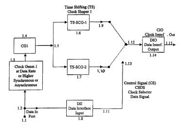
FIG.1 shows a Clock Generation (CG) processor, two Time Shifting (TS)-Signal
Clock Generators (SCG), Data Interface units for Control Signal (CS) Data
Signal (DS)
clock selection of this invention.
FIG. 2 depicts an alternate implementation of Synchronous Clock Recovery-
Clock Generation and of Asynchronous Clock Source (ACS) driven Clock Shaped
(CS)
baseband signals provided to a selection switch for Clock Modulated (CM)
signal
transmission.
FIG. 3 is an illustration of Plural Clock (PCL) generation and selection for
data
controlled information-signal transmission.
FIG. 4 shows an alternate embodiment which includes optional Quadrature
Modulators (QM), PSK or VSB or SSB and PM, FM, QAM or other modulators for
transmission of the Clock Modulated (CM) signals.
FIG. 5 shows and alternative embodiment of Clock Modulated (CM) baseband
signal generation with two Clock Shaper (CS) circuits.
FIG. 6 shows an alternate implementation of an embodiment of a Cross-
Correlated Bit Rate Agile (BRA) system.
FIG. 7 shows an embodiment for a plurality of input signals for a Quadrature
Modulated embodiment of this invention is illustrated, using a Clock Modulated
(CM)
and Bit Rate Agile (BRA) embodiment.
FIG. 8 shows an illustrative Clock Shaped (CS) signal pattern having a
sinusoidal
and a square wave component as its clock elements.
FIG. 9 shows a data pattern generated by one of the embodiments of this
invention, having Clock Shaped (CS) information content, whereby one of the
clock
states has a longer duration while the second clock state has a shorted
duration.
FIG. 10 shows a sample data pattern generated by another embodiment of this
invention having Clock Shaped (CS) information content, whereby one of the
clock
states has a shaped "rounded-off' longer duration while the other clock has a
shaped
rounded off shorter duration.
FIG. 11 shows a sample data information pattern the shorter clock high state
represents the one (1) state, while the longer high state clock the zero (0)
signal -
information state.
CA 02341883 2001-02-27
WO 00/13382 PCT/US99/19909
-13-
FIG.12 illustrates a signal pattern whereby variable amplitude Clock Levels
(CL)
are used for the one and zero states of quadrature I and Q signal patterns.
FIG. 13 shows a sample data pattern and the corresponding Clock Modulated
(CM) - Clock Shaped (CS) baseband signal pattern, generated by one of the
embodiments
of this invention.
FIG.14 depicts an in-phase (I) and a quadature-phase (Q) Clock Modulated (CM)
signal pattern of this invention.
FIG.15 shows an illustrative spectrum having an ultra high spectral
efficiency.
DETAILED DESCRIPTION OF EMBODIMENTS OF THE INVENTION
A detailed disclosure of several implementation architectures and embodiments
of this invention is contained in the following sections. FIG. 1 shows an
embodiment for
Feher Keying (FK) modulations by means of Shaped Clock (SC) signals. In this
architecture the generated SC signals are symmetrical and/or asymmetrical.
Data In Port
1. I accepts incoming data and/or data and clock or sampling signals. Splitter
1.2 provides
the signal and/or clock to units 1.3 and 1.4. Unit I .3 is a Clock Generator
(CG) unit. This
unit provides Data rate or higher or lower clock output than the incoming data
rate of the
signal provided to the input port 1.1. Unit 1.3 provides to Clock Generator
(CGl), unit
1.4 an optional clock signal. Units 1.3 and/or Units 1.4 are optional units.
The output of
1.3 or of 1.4 is split in splitter unit 1.5 and provided to Units 1.6 and 1.7.
The Time
Shaping (TS)-or Time Shifting (TS) Signal Clock Generators (SCG) 1 and 2,also
designated as TS-SCG units, units 1.6 and 1.7 provide Shaped or Shifted Clock
(SC)
signals on leads 1.9 and 1.10 to Control Signal (CS) Data Signal (CSDS)
selector switch
unit 1.12. Signal splitter also provides to Data Interface Input (DII), Unit
1.8 a signal.
This unit processes the input data, received from port 1.1 and
generates/provides the
Control Signal to Selector Switch 1.i2 on lead 1.13. The DII unit 1.8, based
on the data
input pattern generates the CS. In one of the implementations if the data
input at port 1. I
is in a high state then the selector switch selects the shaped clock of lead
1.9, while if the
data input at port 1.1 is in a low state then CS selects the 1.10 lead. The
DII in an other
embodiment generates the CS base on the difference between consecutive one or
more
signal bits present at port 1.1. In a third embodiment the CS generation and
selection of
lead 1.9 or of lead 1.10 is based on the previous bit pattern and/or digital
logic process
algorithms implemented in the DII unit 1.8. Switch 1.12 provides the selected
Shaped
CA 02341883 2001-02-27
WO 00/13382 PCT/US99/19909
- 14-
Clock (SC) to the Data Interface Output (DIO) unit 1.14. The DIO unit provides
the
selected (SC) to the output port 1.15.
Sample data patterns, present at the input port 1.1 are illustrated in FIG. 8
and
FIG. 9. In FIG. 8, signal 8.1 is a representative data signal pattern, pattern
8.2 represents
a pure clock while pattern 8.3 represents an Asymmetrical Shaped Clock (ASC)
pattern.
An other embodiment of FIG.1 processes and generates the sample patterns shown
in
FIG.9. In the aforementioned figure Signal 9.1 is an input data signal,
pattern 9.2 is a
pure clock (the term "pure" implies that the clock is not shaped and or
processed by the
FIG.1 embodiment). Signal 9.3 is a processed clock signal generated by one of
the
embodiments of FIG.1. The 9.3 Shaped Clock (SC) pattern has a "longer " high
state
duration for the one state data pattern and it has " shorter " high state
duration for the zero
state data. Here the terms "longer" and "shorter" are in reference to the
usual prior art
50% on and the 50% off duration clock pulse periods.
FIG. 2 the implementation of the transmit part of an alternate Feher Keying
(FK)
Modulation-Transceiver is shown. The data signal or data information-data
signal at the
input of the FK processor is connected to the "Data Signal Source (DSS) input
port. The
port for DSS, Unit 2.1 provides to units 2.3 and 2.5. The Data In signal or
Data is
provided, to Data Control Encoder (DCE), Unit 2.5. The DCE, provides a control
signal
to the Edge Distance Selection Switch, Unit 2.10 for selection of the shorter
or longer
edge distance clock signals provided by units 2.8 and 2.9.
On lead 2.2 the Data In signal is provided to Data Interface Input (DII) and
Clock
Recovery (CLR) unit 2.3. Unit 2.3 receives on lead 2.2 the data signal and in
the CLR
part of 2.3 recovers a clock signal from the incoming data stream. The CLR
circuit is
implemented by one of the many well known prior art CLR circuit designs
contained and
or referenced in the list of patents and/ publications of this disclosure and
in other
publications. The CLR circuit in one of the implementations generates a Clock
Rate (CR)
output clock signal having the same rate as the incoming data stream at port
2.l.In this
case a synchronous clock, also designated as synchronous equal rate clock-
with that of
the data rate is generated and provided to Selector 2.6. In an other
implementation Unit
2.3 is not used. Instead of the DII and CLR, Unit 2.3, an Asynchronous Clock
Source
CA 02341883 2001-02-27
WO 00/13382 PCT/US99/19909
-15-
(ACL) circuit, Unit 2.4 is used. The ACS circuit is implemented by one of the
many well
known prior art " free-running oscillator "circuit designs contained and or
referenced in
the list of patents and/publications of this disclosure and in other
publications. The
aforementioned oscillator provides a periodic "clock" signal to the lower
input port of
Selector 2.6. The ACL generated clock has a sinusoidal shape in a first
embodiment, in
an second embodiments it has a square-wave clock, in a third embodiment it has
a
triangular clock, in a fourth embodiment it has a filtered or shaped square
wave clock, in
a fifth embodiment the ACL generates a multilevel clock signal while in a
sixth
implementation the ACL provides a processed and filtered multilevel signal to
Selector
2.6. In one of the implementations the "Synchronous-Asynchronous Selector, for
short
Selector, Unit 2.6 is set to select the synchronous clock DII and CLR -Unit
2.3 provided
signal, while in an other implementation it is set to select the ACL Unit 2.4
provided
asynchronous clock. The selected synchronous or asynchronous clock is provided
to
clock signal splitter Unit 2.7 for splitting and connecting the aforementioned
clock (also
designated as "clock signal") to the Shorter Distance Falling Edge Generator
(SFE),Unit
2.8 and to the Larger Distance Falling Edge Generator, Unit 2.9. The SFE and
LFE
generator units process the synchronous or asynchronous clock signal provided
by
Sputter 2.7 by means of conventional prior art processors and generate SFE and
LFE
clocks having sample clock patterns illustrated in FIG. 9, in FIG. 10 and FIG.
11 to
FIG. 14. The aforementioned SFE and LFE clock signals are provide to the Edge
Distance Selection Switch, Unit 2.10 for clock signal selection. The said
switch 2.10
provides on lead 2.12 the selected Clock Modulated (CM) (or also designated as
Converted Clock (CC) signal to the Digital Interface Output (DIO). The Digital
Interface
Output (DIO) and Output port 2.13, shown in FIG. 2, provide the processed
signal to the
transmission medium.
FIG. 3 shows an other alternate implementation and architecture of the FK
transmitter. The Clock Source, Unit 3.1 receives from the Data In port, Unit
3.2 the input
signal to be processed in the FK modulator-transmitter. The Data In port
provides the
Data In signal, in addition to Unit 3.1 also to Data Controller, Unit 3.11.
The said Data
Controller generates a data control signal and provides it to switch 3.12. The
said Data
Controller unit comprises conventional logic and/or memory circuits and
implements a
control signal generation function based on the incoming data pattern. In one
of
CA 02341883 2001-02-27
WO 00/13382 PCT/US99/19909
- 16-
implementations the selector switch 3.12 is selecting one of two clock signals
provided
at ports 3.7 and 3.8. In an other embodiment the data controller 3.11 provides
serial
and/or parallel data to switch 3.12 to select and provide to Interface 3.13
and to output
port 3.14 one signal from a plurality of Clock Shaped (CS) signals at a
specified instant
of time. As an other embodiment example four (4) Clock Shaped signal
processor/generator circuits, designated as CS 1 to CS4 are shown as units
3.3, 3.4, 3.5
and 3.6. The said CS generators have a common input provided by Clock Source
3.1 in
one of the embodiments, while in other designs CS l, CS2, CS3 and CS4 have a
plurality
of dependent or independent, synchronous or asynchronous clock inputs. The CS
generators outputs are provided to ports 3.7, 3.8, 3.9, and 3.10 for the
design case of four
(4) Clock Shaped signal designs. The implemented number of CS processors and
generators is at least one, however it could be two, three, four, five and in
fact any
number. In one of the embodiments the data controller 3.11 compares two
consecutive
data input signal bits or two consecutive data in symbols and based on the
comparison,
if the said bits are different it provides a control signal to switch 3.12 to
select CS 1 and
if said consecutive bits are not different, that is they have the same state,
then it provides
a control signal to switch 3.12 to select CS2. In FIG. 8 a selected clock
signal pattern 8.3
is shown. Depending on the signal-in (also designated as Data In) pattern,
sample pattern
8.1, the Data Controller 3.11 provided control Signal to switch 3.12, selects
the
sinusoidal (SII~ or Square Wave (SQ) clock signal element for transmission.
The time
aligned sequence of the selected said signal elements, forms the shown Clock
Modulated
(CM) clock data pattern 8.3. The said CM clock data pattern has a different
clock signal
element, for the one and for the zero Data-In patterns, or for the difference
between the
consecutive Data-In patterns. The said clock signal elements are also referred
herein and
designated by terms such as clock signal wavelet or clock waveiet or merely
signal
element or clock wavelet or wavelet.
A fundamental, truly pioneering original discovery of this invention is
described
in this part of my patent disclosure. The CM clock pattern 8.3,of FIG. 8,
illustrated as a
sample result of the embodiment of FIG. 3 shows an asymmetrical clock having
different
clock signal shapes. The information to be transmitted is contained in the
shapes of the
clock signals and/or in the different shapes, that is, differences of the
clock signal shapes.
CA 02341883 2001-02-27
WO 00/13382 PCT/US99/19909
-17-
In my previous prior art discoveries, more than 300 publications, co- authored
papers, books and patents as well as in several thousand other prior art
publications and
patents the implementations and designs have been focused on signal shaping of
symmetrical data signaling elements while in this invention the focus is on
signal shaping
of clock signaling elements and in particular of asymmetrical and also of
symmetrical
signaling elements. In the vast majority of prior art systems the data signal
elements have
been processed, shaped and filtered to reduce the spectrum of the data
pattern, while in
this invention, in my aforementioned embodiments, including the embodiment of
FIG.
3 the clock signals have been shaped. Based on my understanding of the prior
art
literature, the Walker inventions and publications, including Walker's [P9;
P10) and [21]
represent an exception as Walker's processors and implementations contain the
information in specific symmetric and synchronous clock time-clock edge
transitions or
specific clock duration/ positions. The prior art literature, including Walker
inventions
do not contain discoveries for asymmetrical binary, synchronous and/or
asynchronous
binary and/or multilevel information transmission whereby the data content-
data
information is contained in shaped clock signals.
FIG. 4 shows an other implementation embodiment and architecture of the Feher
Keying (FK) Modulator and Transmitter. The Data In signal is provided on lead
4.1 to
Data Interface Input (DII) Unit 4.2 The said DII recovers the clock from the
Data In
signal and generates a synchronous clock signal. In an alternate embodiment
instead of
a Clock Recovery and/or synchronous clock generator a free-running
asynchronous clock
generator is implemented. On lead 4.3 the DII processed Data signal is
provided, while
on lead 4.4 the said clock signal is provided. The Clock Converter, Unit 4.6
Clock
Modulates (CM) or clock shapes the pure clock signal and provides synchronous,
asynchronous, symmetrical or asymmetrical binary or multiple state clock
modulated
signals, on lead 4.11 to Converter Unit 4.12. The second and third inputs to
said
converter are provided on leads 4.13 and 4.14 which provide Clock rate and
multiple
M/N clock rate or asynchronous rate clock signals to 4.12. Converter 4.12
shifts the
spectrum of the Clock Converted (CC) or Clock Modulated (CM) signal, provided
on
lead 4.11, based on well established prior art methods. Converter 4.12 is
implemented as
a conventional multiplier and/or any other prior art analog or digital signal
processing
device. Following the converted signal output an optional Filter Unit 4.15 is
CA 02341883 2001-02-27
WO 00/13382 PCT/US99/19909
-18-
implemented. Unit 4.16, designated as Digital Interface Output (DIO) is
implemented in
one of the implementations with digital circuits while in an other embodiment
with
analog circuits, while in a third embodiment with hybrid analog/digital
circuits. The DIO
output lead 4.17 provides a signal to clock signal splitter 4.18. Switches
4.19,4.20 and
4.21 are set to select one or more modulators for transmission. Said
modulators 4.8, 4.9
and 4.10 are conventional Binary DSB modulators, or Quadrature Modulators, or
VSB
or SSB modulators or PM, FM, VCO-FM and or Numerically Controlled Oscillator
(NCO) modulators. In alternate embodiments, instead of said modulators Feher
patented
QPSK, known as FQPSK) or Feher patented Gaussian Minimum Shift Keying
(GMSK),designated as FGMSK or Feher patented QAM {FQAM) is used. The said
modulated signals are provided to one or more output ports 4.22,4.23, and/or
4.24.
FIGS represents an other alternate implementation of this invention. Instead
of
having a binary modulated clock, this embodiment includes a multilevel
asynchronous
and/or synchronous shaped modulated clock implementation embodiment. Data In
Port
5.2 provides on lead 5.5 to Clock Recovery (CLR) unit 5.4 and to Data
Interface Input
(DII), Unit 5.19 signals for further processing. The said CLR circuit is not
used in
asynchronous CM clock generator embodiments as it is replaced by Clock
Generator
{CGl) unit 5.3. Said CG1 is optional for the synchronous mode. If Switch (Swl)
Unit
5.3 is connected to "Ground",Unit 5. l,then CG 1 and the set up is operated in
asynchronous mode; if it is connected to lead 5.4 then a synchronous operation
is
implemented. Switches 5.6 and 5.9 select between signals 5.6,5.7 (ground),5.8
(ground)
and 5.9. Said "Ground" indicates asynchronous or "free -running" mode of the
ground
input connected clock generators. Clock Generator CG2 and CG3Units S.10 and
5.11, as
well as Clock Shapers CSH1 and CSH2 Units 5.14 and 5.18, are connected in the
main
signal path or by-passed (not used-i.e. not implemented) by switch components
5.12,
5.13, 5.16, 5.17 and 5.20. Data Interface Input {DII) Unit 5.19 generates and
provides
Clock Selector Data Signal (CSDS) on lead 5.22 to Switch (Sw8),Unit 5.21. The
selected
Clock Modulated Signal is provided to Data Interface Output 5.23 for interface
circuit
embodiment to output lead 5.24.
FIG. 6 and FIG. 7 implementation and embodiment contains components
described in Feher' s other pending patents K. Feher, Ref.[PP2 to PPS]. A
fundamental
CA 02341883 2001-02-27
WO 00/13382 PCT/US99/19909
-19-
difference between the Referenced [PP2 to PPS] embodiments, use, design and
applications is that the Control Signal 104,CTL and SAM 105 and 106 leads, of
this
invention, See FIG. 7 contain Clock Modulated Signals and that the data
information is
processed and transmitted and received, demodulated by processors which
contain clock
modulation clock shaping and or asynchronous and synchronous binary and
multilevel
clock modulated signals, described in conjunction with previous figures of
this new
patent application. In FIG. 6. most or all Clock Signals of this invention
contain Clock
Modulated (CM) and or Clock Shaped (CS) clock signals, including symmetrical,
asymmetrical binary, multilevel and asynchronous signals while in Ref.[PP2 to
PPS] pure
not shaped not clock modulated clocks are used for clocking-designated as "C"
signals
or "C" clocks and numerous units of FIG. 6 as well as FIG. 7.
In FIG. 6 an implementation diagram with cascaded switched transmit (Tx) and
receive (Rx) Low-Pass- Filters (LPF) in conjunction with cross-correlated and
other non
cross-correlated TCS response and cascaded LR processors is shown. These LR
processors could be implemented as separate I and Q LPF s or as an individual
time-
shared LPF. The Transmit Baseband Signal Processor (BBP) including the I and Q
LPF
s could be implemented by digital techniques and followed by D/A converters or
by
means of analog implementations or a mixture of digital and analog components.
External Clock and External Data Signals are used to drive the S/P and the
entire
baseband processor (BBP). The BBP may include a Differential Encoder (DE). The
I and
Q LPFs may be implemented as single filters (instead of cascaded filters).
Modulation
and Demodulation filters have been implemented and tested with intentionally
Miss-
Matched (MM) filter parameters. LR filters have been synthesized and
implemented as
phase equalized and non-equalized phase response transmit and receive Bessel,
Gaussian,
Butterworth and Chebycheff filters. Bessel, Gaussian and Butterworth and
Chebycheff
filters as well as other classical filters are within the previously described
and defined
class of Long Response (LR) filters. These filters have a relatively long
practical impulse
and/or pulse response. The measurable practical pulse response of the
aforementioned
filters having an approximately BTb=0.5 design parameter extend to many bit
durations.
Here B refers to the 3dB cut-off frequency of the filter and Tb to the unit
bit duration.
From classical communications and Nyquist transmission theory it is well known
that the
theoretical optimal performance minimum signal bandwidth is defined for
BTb~.S. The
CA 02341883 2001-02-27
WO 00/13382 PCT/US99/19909
-20-
LPFs in the I and Q channels, or the shared single set of LPFs,
implementations include
Infinite Impulse Response (IIR) and Finite Impulse Response (FIR) filters.
In FIG. 6 on lead 6.3 a serial data stream is present. This signal is provided
to
6.4a and the optional 6.4b units for Serial-to-Parallel (S/P) conversion and a
lbit duration
(Tb) offset in one of the implementations. In other implementations there is
no offset
delay 6.4b in the embodiment. Some other alternate embodiments use a
selecteable offset
delay 6.4b which is larger or equal to zero and smaller than the duration of
approximately
200 bits. As stated the Offset logic is used in certain embodiments, while in
other
architectures it is not present. The input signal or input signals are
provided on leads 6.1
and 6.2 instead of lead 6.3 in some of the alternative implementations of this
invention.
Unit 6.5 is a Base-Band Processor. Unit 6.5 may be clocked, controlled and
sampled by
signals such as C, CTL, and SAMP such as illustrated previously in FIG. 1 to
FIG. 3.
In this figure, FIG. 6, all of these clocking, control and sampling signals
which could
represent multiple rates and multiple leads are collectively or individually
abbreviated
simply as "C" and illustrated with an arrow near the letter "C." Unit 6.5 in
some of the
embodiments performs the Time Constrained Signal (TCS) processing, waveform
assembly and generation fimctions of multiple symbol TCS cross correlation and
signal
processing operations. The I and Q outputs of unit 6.5 are provided as inputs
to the
transmit set of LPFs designated as TX1 LPF-1 unit 6.6 and TXQ LPF-1 unit 6.11.
This
set of first LPFs could be cascaded with a second set of I and Q channel LPFs
units 6.7
and 6.13. Switch units 6.8 and b.12 illustrate that the second set of LPFs
could be
bypassed and/or deleted in some of the embodiments.
The LR filter units, embodied by the first and second sets .of I and Q are
implemented as LPFs or alternately as of other types of filters such as Band-
Pass Filters
(BPF) or High Pass Filters (HPF) or other filter/processor LR filter
combinations. As
stated previously, for several embodiments all of the aforementioned
processors are BRA,
while for other implementations bit rate agility may not be required. Units
b.9, 6.10, 6.14,
6.15 and 6.16 comprise a quadrature modulator in which the I and Q modulators
are 90-
degree phase shifted and in which a Local Oscillator (LO) is used as a Carner
Wave
(CW) generator. Unit 6.17 is an amplifier that could be operated in a LIN or
in a NLA
mode. The output of amplifier 6.17 is provided on lead 6.18 to the
transmission medium.
CA 02341883 2001-02-27
WO 00/13382 PCT/US99/I9909
-21 -
In FIG. 6 at the receiving end, on lead 6.19, is the received modulated
signal.
Unit 6.21 is a BPF that is present in some embodiments while in others it is
not required.
Alternatively the receive BPF could be "switched-in" or "switched-out" by
switch 6.20.
In some implementations Surface Acoustic Wave (SAW) BBF were used to implement
6.21. Units 6.22, 6.23, 6.24 and 6.25 embody a Quadrature Demodulator (QD)
with a
corresponding Local Oscillator (LO). The aforementioned LO represents for some
embodiments an entire Carner Recovery (CR) subsystem while for other
embodiments
it is a free running LO. The set of LPFs 6.26 and 6.27 are the embodiment of
post-
demodulation filters, while the second set of LPFs 6.28 and 6.29 may be used
to further
enhance the spectral efficiency advantages or other performance advantages of
designed
systems. The second set of LPFs could be connected or disconnected by switches
6.30
and 6.31 or entirely deleted. Unit 6.32 is the Clock Recovery (CR) andlor
Symbol Timing
Recovery (STR) system. For fast clock and/or STR, this unit is connected in
some of the
embodiments in parallel to the Carrier Recovery (CR) subsystem. In one of the
embodiments of fast Clock Recovery (CR) systems, the parallel configuration
embodied
by units 6.37 and 6.38 is used for discrete signal clock generation. The
discrete signal
spike, in the frequency domain, provides on lead 6.39 the clock recovery unit
6.32 with
a discrete spectral line signal which is exactly at the symbol rate or at the
bit rate. In this
architecture unit 6.37 is a multiplier or any other nonlinear device which has
at its input
the received modulated signal and the same received modulated signal
multiplied by a
delayed replica of itself. The aforementioned delayed replica is generated by
unit 6.38,
a delay element. The receiver structure, shown in FIG. 6, is one of the many
possible
alternative receiver and demodulator structures. It is inter-operable
compatible and
suitable for BRA and MFS and CS reception, demodulation and/or decoding of the
transmitted signals embodied by means of the BRA and/or MFS and/or CS
implementation of the FIG. 6 transmitter embodiments.
Contrary to the teachings and wisdom of well established communication theory,
of matched filter-optimal demodulation theory and optimal data reception
theories, in
several embodiments of the current invention, substantially Miss-Matched (MM)
modulator and the demodulator filters have been implemented. Fundamental and
pioneering discoveries, regarding the cascaded pulse response of TCS response
and of
CA 02341883 2001-02-27
WO 00/13382 PCT/US99/19909
-22-
LR filter cross-correlated BRA implementations of modulator I and Q f lters
and that of
the implementations of "matched " and/or intentionally " Miss-Matched" (MNI)
demodulator filters are disclosed in this part of the invention. In classical
communication
theory the demodulation LPFs, and in fact the entire cascaded receiver and
demodulation
filter responses are matched to the characteristics of the modulator and
entire cascaded
modulator and RF transmitter filters. The intentionally and substantially Miss-
Matched
(IVfiVI) transmit and receive filter designs, used in implementations of this
invention lead
to simpler implementations than implied by communication matched filter theory
and to
substantially improved performance for RF power efficient NLA transceivers.
From
communications theory, numerous books, referenced publications as well as fibm
patents
it is well known that for "optimum" performance the cascaded filters of the
modulator
should be matched by the cascaded receive demodulator filters. For example, in
a
conventional bandlimited QPSK system, if Nyquist filters are implemented as "
raised
cosine filters", then the best "optimal" performance is attained if the
cascaded transmit
and receive filters have a raised cosine transfer function and the filtering
is equally split,
i.e. "matched " between the transmitter and receiver. For pulse transmission,
such as
filtered NRZ data an aperture equalizer, having an wTs/ sin(wTs) frequency
response is
used in theoretical optimal transmitters, prior to the implementation of the
transmit
matched filter. Specifically, based on Nyquist transmission and filter
theories, combined
with matched filter receiver theories the 3dB cut-off frequency of an optimal
minimum
bandwidth transmit filter, used as a baseband I or Q channel filter, in a QPSK
system
equals %z of the symbol rate or alternatively'/4 of the bit rate. The 3dB
bandwidths of the
modulator and demodulator filters of the "theoretical optimal" bandlimited
QPSK system
are matched. The 3dB bandwidth of the theoretical optimal system it is the
same for the
modulator filter and for the demodulator filter. If these filters are
implemented by pre-
modulation LPFs and post-demodulation LPFs then the aforementioned theoretical
bandwidth corresponds to BTs~.S. This value corresponds to BTb=0.25, where B
is the
3dB bandwidth of the respective filters, Ts is the unit symbol duration and Tb
is the unit
bit duration.
Contrary to the teachings of the aforementioned optimal performance matched
filter modulation demodulation theory, we disclose the implementation of
demodulator
architectures and embodiments with "Miss-Matched" (MM) filtering. The term
Miss-
CA 02341883 2001-02-27
WO 00/133$2 PCT/US99/19909
-23-
Match (MM) refers to intentional and substantial MM between the cascaded 3dB
bandwidth of the I and Q demodulator filters with that of the cascaded
response of the
modulator I and Q filters. Alternate embodiments include MM pre-modulation
baseband
LPF and post-demodulation baseband LPF designs as well as post modulation BPF
transmitter implementations and receiver pre-demodulation BPF implementations.
A
combination of the aforementioned baseband and BPF designs has been also
implemented. The term "substantial " MM in a BRA architectures and embodiments
such
as shown in the FIG. 6 discloses a processor architecture and embodiment of
the FK
processor. The Data in Port is connected to the Data Interface Input (DII)
system, which
provides Clock Selector Data Signal (CSDS) to Switch 8 (Sw 8). The DII means
determines which Clock Generator (CG) shape signal and Clock Shaper (CSH) is
selected, based on the Data Input Pattern and the specific Encoder of the DII.
The Data
In Port may be connected to an option Clock Recovery (C1R)* system. Clock
Generator 1
(CGl) may be free-running as indicated if Switch 1 (Swl) is connected to
Ground. In this
case, asynchronous, i.e., non-synchronous, clock generation relative to the
Data Input is
used. Alternatively, CGI may operate in synchronism with the Data In Port. The
Clock
Shaping circuits, CShI and CSh2, provide asynchronous or synchronous signals
having
the same type or completely different type of Shaped Clock Signals to the Data
Interface
Output (DIO) circuit.
FIG. 7 implementation and embodiment contains components described in Feher'
s other pending patents K. Feher, Ref.[PP2 to PPS]. A fundamental difference
between
the Referenced [PP2 toPPS] embodiments, use, design and applications is that
the
Control Signal 104, CTL and SAM 105 and 106 leads, of this invention (See FIG.
7),
contain Clock Modulated Signals and that the data information is processed and
transmitted and received, demodulated by processors which contain clock
modulation
clock shaping and or asynchronous and synchronous binary and multilevel clock
modulated signals, described in conjunction with previous figures of this new
patent
application. In FIG. 6. most or all Clock Signals of this invention contain
Clock
Modulated (CM) and or Clock Shaped (CS) clock signals, including symmetrical,
asymmetrical binary, multilevel and asynchronous signals while in Ref. [PP2 to
PPS]
pure not shaped not clock modulated clocks are used for clocking-designated as
"C"
signals or "C" clocks and numerous units of FIG. 6 as well as FIG. 7.
CA 02341883 2001-02-27
WO 00/13382 PCT/US99/19909
-24-
FIG. 8 FK clock modulated sample patterns including Data In pattern, Pure
Clock, Clock for 1 state, Clock for 0 state, selected clock-modulated output
patterns are
illustrated. The specific patterns 8.1,8.2 and 8.3 were described previously
in this
applications and for this reason their description will not be repeated here.
In FIG. 9 Clock shaped data patterns following one of the Clock Shaping
Processing (CSP) generated by a clock shaped subsystem are illustrated. The
specific
patterns 9.1, 9.2, and 9.3 were described previously in this application and
for this reason
their description will not be repeated here.
FIG. 10 shows a data pattern 10.1 a pure clock pattern 10.2 and shaped
asymmetrical clock patterns 10.3 and 10.4 generated by Clock Shape circuits of
this
invention. An illustrative resulting clock shaped selected output clock
modulated signal
is represented by clock signal 10.5
FIG.11 shows an illustrative input Data-In pattern 11.1, a pure clock pattern
11.2
and a Shorter and Longer Duration processed clock pattern 11.3 and 11.4 as
well as the
selected Converted Clock (CC) pattern 11.5 generated by one of the embodiments
of this
invention. In this case a data signal with a Shorter (S) falling edge distance
from that of
the rising clock edge represents the "1" state, while the "0" state has a
larger (L) distance.
FIG.12 shows a shaped clock at the in-phase (I) and at the Quadrature Phase
(Q)
ports of an embodiment such as the embodiments of FIG. 6 and FIG. 7.
FIG.13 shows a data pattern 13.1 and a corresponding shaped Clock Modulated
(CM) signal pattern 13.2 generated by the designs of this invention.
FIG.14 shows alternate clock modulated data patterns 14.1 by embodiments of
this invention to 14.4 at various ports of Quadrature I and Q modulator,
generated and
a corresponding shaped Clock Modulated (CM) signal pattern 13.2 generated by
the
designs of this invention.
CA 02341883 2001-02-27
WO 00/13382 PGT/US99/19909
-25-
FIG. 15 illustrates one of the ultra spectral efficient FK modulated signals
which
has a spectral efficiency of approximately 30b/s/Hz up to the -28dB power
spectral
density attenuation points.
Acisliirit~i~.tiQn
Having now described numerous embodiments of the inventive structure and
method in connection with particular figures or groups of figures, and having
set forth
some of the advantages provided by the inventive structure and method, we now
highlight some specific embodiments having particular combinations of
features. It
should be noted that the embodiments described heretofore, as well as those
highlighted
below include optional elements or features that are not essential to the
operation of the
invention.
A first embodiment ( 1 ) provides a structure comprising a shaped clock signal
generator means said shaped clock generator being synchronous or asynchronous
with
the data bit rate received by a data signal receive input port; and a data
signal receiver
port and processor for providing control signal generation means for selecting
the said
shaped clock signal for further transmission and/or modulation.
A second embodiment (2) provides a structure comprising a splitter receiving
an
input signal and splitting said input signal into two or more signal streams;
a clock
generator for receiving one of the said signal streams and generating a clock
signal;one
or more shaped clock generator means for receiving said clock signal and for
generation
of one or more shaped clock signals; a set of input ports for receiving shaped
clock
signals; a selector switch for selecting one of the shaped clock signals, said
selector
switch having an input interface port connected to the data-based selection
control signals
and another set of input ports connected to the shaped clock signals; and an
output
interface port coupled to said selector switch output.
A third embodiment (3) provides an architecture comprising a data interface
input
for receiving input data and for providing an input data-based clock selector
data signal;
a set of input ports for receiving a set of shaped clock signals and of not-
shaped clock
signals; a set of one or more clock generators which differ in one or more
clock
CA 02341883 2001-02-27
WO 00/13382 PCT/US99/19909
-26-
parameters from each other; a selector switch for selecting one of the
processed clock
signals; and a data interface output port for receiving said selected signal
and providing
it to the transmitter circuitry.
A fourth embodiment (4) provides a structure comprising a clock generator
which
provides clock signals to two or more clock transition time shifting and clock
shaping
signal generators; a data input port and connection to a data interface input
encoder for
the generation of clock selector data signal by said data input interface
encoder; a switch
to choose, based on said clock selector data signal, one of the clock
transition time-
shifted shaped clock signals and connect the selected signal to the data
interface output
unit; and a data interface output unit for connecting the selected signal to
the transmission
medium or further signal processing.
A fifth embodiment (S) provides a transmit signal processor structure
comprising
a first clock signal generator having a first set of clock shaping parameters;
a second
clock signal generator having a second set of clock shaping parameters, said
second set
of clock shaping parameters having at least one parameter different from that
of the first
set of clock signal shaping parameters; a data input receive circuitry and
processor for
selection of one of the said first or second clock shaped signals; a switch
for switching
between the first set and second set of shaped clock parameters; and an output
interface
port to provide the selected signal to the transmission medium.
A sixth embodiment (6) provides a spectral saving data and clock signal
processing system comprising data signal and clock signal processing means to
provide
a clock modulated signal having changeable distances between the rising edges
and
falling edges of the modulated clock signals; control means having its input
connected
to the data signal source and its output connected to edge distance switch
selection
means; and digital interface output means to connect the clock modulated
signal to the
interface of the subsequent signal processor.
A seventh embodiment (7) provides a clock signal modulator comprising a data
input interface means to provide data signals to an asynchronous pure clock
source; an
asynchronous pure clock generator means to provide a pure clock signal; and a
selector
CA 02341883 2001-02-27
WO 00/13382 PC'T/US99/19909
-27-
switch means which is controlled by the data interface means to provide a
shorter
distance between the falling edge and rising edge of the clock modulated
signal for a zero
state data signal and a longer distance between the falling edge and rising
edge of the
clock modulated signal for a one-state data signal.
An eighth embodiment (8) provides a clock converter system comprised of an
input data interface means for controlling the selection process of the shaped
clock signal
which is provided to the interface output unit means; a clock signal shaping
means to
provide smoothed continuous clock signals to the clock signal selection means
having
one or more different clock signal parameters; and an output signal processing
means to
accept the smoothed different clock signal parameter processed clock converted
signals.
A ninth embodiment (9) provides a clock modulated signaling system comprising
an input data interface means to provide control signal generation and
selection means
of shaped clock signals; an interface means to provide signal processing means
for
modulating the clock modulated baseband signal by means of a cross-correlated
quadrature modulator system; an output amplifier means to connect the cross-
correlated
quadrature modulated signal to the transmission medium; demodulation means to
demodulate the received quadrature modulated signal; and signal processor
means to
decode and regenerate the clock modulated signal.
A tenth embodiment ( 10) provides an architecture comprising a data interface
input for receiving input data and for providing an input data-based clock
selector data
signal; a set of input ports for receiving a set of shaped clock signals and
of not-shaped
clock signals; a set of one or more clock generators which differ from each
other in one
or more clock parameters; a selector switch for selecting one of the processed
clock
signals; and a data interface output port for receiving said selected signal
and providing
it to the transmitter circuitry.
An eleventh (11) embodiment provides a method comprising steps: receiving a
data signal; generating a shaped clock signal in response to the received data
signal;
generating a control signal for selecting the generated shaped clock signal;
and
processing the selected shaped clock signal for transmission or modulation. A
twelfth
CA 02341883 2001-02-27
WO 00/13382 PCT/US99/19909
-28-
( 12) embodiment further provides that the shaped clock signal is generated
synchronously
with a data bit rate of the received data signal. A thirteenth (13) embodiment
alternatively provides that the shaped clock signal is generated
asynchronously with a
data bit rate of the received data signal.
A fourteenth (14) embodiment provides a method of signaling using clock
modulated signals, the method comprising: selecting at least one shaped clock
signal;
cross-correlating and quadrature modulating the selected at least one shaped
clock signal;
amplifying the cross-correlated quadrature modulated signal; transmitting the
amplified
cross-con elated quadrature modulated signal; receiving the transmitted
amplified cross-
correlated quadrature modulated signal;demodulating the received signal; and
decoding
the received demodulated signal and regenerating the clock signal.
Other embodiments provide methods that implement and/or effectuate the
processing performed by the above described structures, and yet other
embodiments
provide computer programs and computer program products that embody the
inventive
methods.
The foregoing descriptions of specific embodiments of the present invention
have
been presented for purposed of illustration and description. They are not
intended to be
exhaustive or to limit the invention to the precise forms disclosed, and
obviously many
modifications and variations are possible in light of the above teaching. The
embodiments were chosen and described in order to best explain the principles
of the
invention and its practical application, to thereby enable others skilled in
the art to best
use the invention and various embodiments with various modifications as are
suited to
the particular use contemplated. It is intended that the scope of the
invention be defined
by the claims appended hereto and their equivalents.