Note: Descriptions are shown in the official language in which they were submitted.
CA 02341894 2001-02-27 i
- 1 -
Method and device for preparing and/or analyzing
biochemical reaction carriers
Description
The invention relates to the use of an illumination
matrix which can be controlled to generate an
optionally adjustable exposure pattern, in particular a
programmable light source matrix, in the field of
biotechnology in general and for preparing,
manipulating and analyzing opto-fluidic reaction
carriers in particular.
Miniaturizing and at the same time functionally
integrating elements, components and whole systems make
novel applications available in many technologies. Said
applications extend from sensor technology via
microsystem technology (e. g. complex biochips using
semiconductor technology) to actuator technology (e. g.
in the form of micropumps). The industries extend from
classical mechanical engineering via automotive and
aviation industries to medical technology and the
forward-looking biotechnology. In medical technology,
for example, new implants are developed and the
pharmaceutical industry advances new technologies for
efficient development of novel medicaments and
diagnostic systems at enormous cost. Owing to its great
potential, biotechnology in particular profits from
said development.
Novel methods which make use of the changed peripheral
conditions are developed for economical production in
the field of microtechnology. The same is true for the
inspection techniques required for monitoring the
miniaturized processes.
For basic research in the life sr_iences and for medical
diagnostics and some other disciplines, gathering
biologically relevant information (mostly in the form
CA 02341894 2001-02-27
- 2 -
of genetic information) in defined examination material
is extraordinarily important. In this context, the
genetic information is present in the form of an
enormous variety of different nucleic acid sequences,
the DNA (deoxyribonucleic acid). Realization of said
information leads, via producing transcripts of DNA
into RNA (ribonucleic acid), mostly to the synthesis of
proteins which for their part are commonly involved in
biochemical reactions.
A powerful system format for gathering said wealth of
information is the so-called biochip. Biochips in this
connection mean highly miniaturized, highly parallel
assays. Detecting particular nucleic acids and
determining the sequence of the four bases in the
nucleotide chain (sequencing) produces valuable data
for research and applied medicine. In medicine, it was
possible, to a greatly increasing extent through in-
vitro diagnostics (IVD) , to develop and provide to the
doctor in charge equipment for determining important
patient parameters. For many diseases, diagnosis at a
sufficiently early stage would be impossible without
said equipment. Here, genetic analysis has been
established as an important new method (e. g. case
diagnosis of infectious diseases such as HIV or HBV,
genetic predisposition for particular cancers or other
diseases, or in forensic science). Close interaction
between basic research and clinical research made it
possible to elucidate the molecular causes and
(pathological) connections of some diseases down to the
level of genetic information. This development,
however, has only just started, and greatly intensified
efforts are necessary, particularly for the conversion
into therapy strategies. Overall, the genome sciences
and nucleic acid analysis connected therewith have made
important contributions both to the understanding of
the molecular bases of life and to the elucidation of
very complex diseases and pathological processes.
Moreover, genetic analysis or analysis through genetic
CA 02341894 2001-02-27
- 3 -
engineering already now provides a broad spectrum of
diagnostic methods.
Further development in medical care is hampered by the
explosion in costs related to correspondingly expensive
methods. Thus, determining genetic risk factors by
sequencing at the moment still costs several hundred to
several thousand US dollars. It is necessary here not
only to demand implementation of possible diagnostic
and therapeutic benefits, but also to advance
integration into a workable and affordable health-care
system.
Likewise, applying appropriate techr_ologies in research
can take place on a large scale and also at
universities only if the costs related thereto are
reduced. Here, a change in paradigms of research in
life sciences begins to emerge:
The bottleneck of deciphering primary genetic
information (sequence of bases ir: the genome) and
detecting the state of genetic activity (genes
transcribed into messenger RNA) of cells and tissues is
removed by the availability of sufficiently cheap,
powerful and flexible systems. It is then possible to
concentrate- work on the (very complex) task of
analyzing and combining the relevant data. This should
result in new levels of knowledge for biology and
subsequently in novel biomedical therapies and
diagnostic possibilities.
The biochips already mentioned before are miniaturized
hybrid functional elements with biological and
technical components, for example biomolecules which
are immobilized on the surface (outer surface or/and
inner surface) of a carrier and which may serve as
specific interaction partners, and a matrix, for
example silicon matrix. Frequently, the structure of
said functional elements has rows and columns; this is
CA 02341894 2001-02-27
- 4 -
known as a chip array. Since thousands of biological or
biochemical functional elements may be arranged on such
a chip, microtechnical methods are usually needed to
prepare said elements.
Essentially, two principles are used as methods for
preparing said arrays: application of finished probes
or functional elements to the reaction carrier, which
is the predominantly used method at the moment, or in-
situ synthesis of the probes on the carrier. The
devices used for both principles are so-called
microfluidic spotters. In-situ synthesis may also use
photolithographic methods.
Possible biological and biochemical functional elements
are in particular: DNA, RNA, PNA, (in nucleic acids and
chemical derivatives thereof, for example, single
strands, triplex structures or combinations thereof may
be present), saccharides, peptides, proteins (e. g.
antibodies, antigens, receptors), derivatives of
combinatorial chemistry (e. g. organic molecules), cell
components (e. g. organelles), cells, multicellular
organisms, and cell aggregates.
A multiplicity of photolithographic systems for
exposure-dependent generation of fine and very fine
structures using light of different wavelength (energy)
of down to below 200 nm are commercially available for
applications in semiconductor technology. The finer the
structures to be generated, the shorter the wavelength
used has to be. Thus, structures in the sub-~,m range
which are already in the range of visible-light
wavelengths (400-800 nm) can only be generated using
high energy radiation of distinctly shorter wavelength.
Photolithographic systems consist in principle of a
lamp as energy or light source and a photolithographic
mask which has transparent and nontransparent areas and
thus generates an exposure pattern in the transmitted-
light course of ray. Optical elements reproduce said
CA 02341894 2001-02-27
exposure pattern on the object to be exposed (e. g.
reduced by a factor of 100). A line on the mask is
thereby reduced in width from 0.1 mm to 10 Vim.
Preparing a microstructure in or on a silicon wafer
commonly requires 10 to 30 exposure steps. The systems
are geared to said number and facilitate automatic mask
switching by means of magazines and operating tools.
Thus, an almost macroscopic structure of the mask
results in a microstructured image on the object to be
exposed, for example the silicon wafer. To generate a
photolithographic mask, photolithographic systems are
likewise employed again which, of course, need only a
correspondingly lower resolution and also, depending on
the preparation method, only a correspondingly smaller
energy input. This is a cyclic process which has been
very far advanced and perfected due to the large market
volume of the semiconductor industry.
GeSim already uses for the production of
photolithographic masks LCD photo plotters from
Mivatec. This is possible, since the mask structures,
with respect to structure size and required wavelength,
allow exposure in the visible-light range. This makes a
relatively fast and relatively flexible production of
masks possible. This is sufficient in semiconductor
technology owing to the limited number of masks
required, since only a functional test shows the
success of the microstructuring and thus there is
usually always enough time for producing new or
improved masks. Overall however, producing the masks is
expensive, time-consuming and not. very flexible.
Using photolithography for the light-induced in-situ
synthesis of DNA (synthesis directly on the biochip),
Affymax Institute and Affymetrix already use commercial
exposure systems for preparing high-density DNA
microarrays (references: US 5,744,305, US 5,527,681,
US 5,143,854, US 5,593,839, US 5,405,783). The
CA 02341894 2001-02-27
- 6 -
wavelength employed is restricted to 300-400 nm. Each
change in the exposure pattern requi res a mask change.
This is extremely restricting sir_ce preparing, for
example, a DNA array with oligcrucleotides of 25
building blocks in length (25-mers) per slot requires
approx. 100 individual exposure cycles.
In general, the reaction carriers have a 2D base area
for the coating with biologically or biochemically
functional materials. The base areas may also be
formed, for example, by walls of one or more
capillaries or by channels. An extension of the
geometry is a 3D structure in which analyzing and,
where appropriate, also manipulating or controlling the
reactions take place in a 2D arrangement.
Especially in the USA, enormous resources are used to
advance the development of miniaturized biochips.
Regarding the prior art, the following publications are
referred to, for example:
1. Nature Genetics, Vol. 21, supplement (complete),
Jan. 1999 (BioChips)
2. Nature Biotechnology, Vol. 16, pp. 981-983, Oct.
1998 (BioChips)
3. Trends in Biotechnology, Vol. 16, pp. 301-306,
Jul. 1988 (BioChips).
Important application fields for mir_iaturized, parallel
assays and thus for applying the present invention are:
molecular diagnostics (including in-vitro diagnostics,
clinical diagnostics, genetic diagnostics)/development
of pharmaceuticals (substance development, testing,
screening etc.)/biological basic research (i.a.
genomics, transcriptomics, proteomics, physiomics)/-
molecular interactions/analysis and screening of
pathogens (viroids, prions, viruses, prokaryotes,
CA 02341894 2001-02-27
_ ') -
eukaryotes)/oncology/environmental monitoring/food
analysis/forensic science/screening of medical products
(i.a. blood products)/detection, analysis and screening
of transgenics (plants, animals, bacteria, viruses,
breeding, outdoor trials)/cytology (i.a. cell
assays)/histology/all types of nucleic acid analyses
(i.a. sequence analysis, mapping, expression
profiles)/SNPs/pharmacogenomics/functional genomics.
The object of the invention is to provide a method and
a device which facilitate relatively flexible and
relatively fast preparation and relatively efficient
analysis of miniaturized highly parallel reaction
carriers.
Method and device should in addition facilitate
integration of preparation and analysis into one
apparatus. Furthermore, it is intended to create a
basis for completely automating all processes in
preparation and analysis.
The method of the invention for preparing a reaction
carrier coated with biologically or biochemically
functional materials comprises the following steps:
(a) providing a carrier having a surface which has
photoactivatable groups,
(b) activating the photoactivatable groups on at least
one predetermined area of the carrier surface by
location-specific exposure of the carrier using an
illumination matrix which can be controlled to
generate an optionally adjustable exposure
pattern,
(c) location-specific binding of biologically or
chemically functional materials or building blocks
for such materials on at least one of the
predetermined areas and
(d) where appropriate, repeating the activation and
binding steps on the same or/and different
CA 02341894 2001-02-27
_ g _
predetermined areas.
The carrier is a solid phase which can be or is
equipped with biochemical or biological materials or
receptors or building blocks thereon. The carrier may
have a planar surface or a surface provided with
grooves, for example channels. The channels are
preferably microchannels of, for example, from 10 -
1000 ~.m in cross section. The channels may be -
depending on the surface properties - capillary
channels but also channels without capillary action
(e. g. owing to Teflon coating?. The carrier is at least
partially optically transparent in the area of the
reaction areas to be equipped.
The use of an illumination matrix which can be
controlled to generate an optionally adjustable
exposure pattern, facilitates great flexibility in the
preparation or/and manipulation or/and analysis of
opto-fluidic reaction carriers and, in particular,
faster preparation of reaction carriers than previously
possible. In contrast to generating correspondingly
fine-resolution exposure patterns in a photolithography
machine by means of invariant individual masks which
have to be changed when changing the exposure pattern,
using a controllable illumination matrix can in
principle generate and alter any possible exposure
pattern by simply controlling the illumination matrix
from a control computer. Thus, in one production
process it is in principle possible to generate and
analyze in one day hundreds to thousands of different
reaction carriers having a multiplicity of individual
reaction areas, something which has been impossible up
until now.
The predetermined reaction areas for which a location-
specific exposure of the carrier is to be carried out
are selected for an actual application preferably
automatically by a program -,~hich facilitates
CA 02341894 2001-02-27
g _
controlling and assigning the reaction areas to one or
more reaction carriers according to the criteria
synthesis efficiency, optimal synthesis conditions, for
example temperature etc., optimal analysis conditions,
for example hybridization temperature with respect to
neighboring areas. After preparing the carrier, it may
be provided for, where appropriate, to change the
carrier and to continue the process from step (a)
onward. In this context, step (c) may include the
location-specific binding of biologically or chemically
functional materials or building blocks for such
materials in the same way as in the preceding cycle or
else taking into account the information from a
preceding synthesis cycle.
Programmability and electronic controllability of the
illumination matrix remove the exchange and also
generation of the mask units as were required for the
photolithographic methods. Generating the exposure
patterns thus is no longer connected with expenses for
preparing, exchanging, positioning, storing and
optimizing exposure masks. This makes in particular the
in-situ synthesis of reaction carriers (e.g. DNA
microarrays) accessible to wide use. According to a
preferred embodiment of the invention, an illumination
matrix is used which is able to illuminate with a
resolution of at least 500 points per cm2.
The illumination matrix and the assigned light source
serve in principle to provide the desired exposure
pattern for controlling/exciting photochemical
processes or, where appropriate, for analyzing a
reaction carrier matrix. According to a variation, it
is possible to optionally modulate the light intensity
and/or wavelength of each luminous spot of the
illumination matrix or of the exposure pattern on the
reaction carrier.
The illumination matrix used is preferably a
CA 02341894 2001-02-27
- 10 -
controllable reflection matrix which reflects light
location-selectively, according to its control, in a
particular direction (here in the direction of the
reaction carrier). Such reflecting surface light
modulators having controlled deformable mirror
arrangements for generating light catterns can be in
particular light modulators having viscoelastic control
layers or light modulators having micromechanical
mirror arrays. Regarding the technclogy of such light
modulators having viscoelastic control layers and light
modulators having micromechanical mirror arrays,
relevant data sheets of the Fraunhofer Institute for
Microelectronic Circuits and Systems are referred to
and are attached to this application. The advantage of
such controllable reflection matrices is in particular
that they are available for a wide spectral range from
W to IR light, for example in a wavelength range from
200-2000 nm. The newest developments of controllable
reflection matrices in 40V-CMOS technology are
advantageous in particular for transmitting high-energy
radiation in the W range and also in general at high
energy densities per area. Due to the working voltage
of 40 V, the matrices are correspondingly insensitive.
A further advantage is that a reflection matrix of this
type facilitates an exposure parallel in time of all
sites to be exposed in the exposure pattern at
appropriate illumination using a light field extending
across the matrix area. This possibility of parallel
exposure of a reaction carrier has consequences for the
length of the preparation (for in-situ syntheses), for
the possibilities of online control and evaluation (no
artefacts due to time gaps between points of
measurement etc.) and for possible manipulations, for
example in the case of cell arrays or other biological
components of a reaction carrier (for example in the
case of retina preparations or light-dependent neuronal
activity).
As long as parallel exposure is not crucial, it is
CA 02341894 2001-02-27
- 11 -
possible, instead of uniform il~.~umination of the
illumination matrix to carry out screening or scanning
of the illumination matrix using a bundled beam, for
example a laser beam, in order to generate the desired
light pattern on or in the reaction carrier, according
to the control of the illumination matrix. It is thus
possible to utilize a wide variety of light sources,
for example also light sources whose emission spectrum
or emission wavelength can be optionally altered, e.g.
an Nz laser, so that, for example, a plurality of
signal-generating fluorescent substances on or in the
reaction carrier can be excited using different
wavelengths (this is a kind of 2D spectroscopy).
Another class of possible illumination matrices for the
use according to the present invention is represented
by light source arrays, i.e. matrix-like arrangements
of very small light sources which can be controlled
individually. These can be, for example, microlaser
arrays, microdiode arrays or the like. W-light
emitting diodes are available now whose emission
wavelength is 370 nm. Such UV-light emitting diodes are
sold under the type designations NSHU 590 and NSHU 550
by Roithner Lasertechnik, A-1040 Vienna,
Fleischmanngasse 9. The corresponding W-light emitting
diode technology can be used for preparing a diode
array, in particular microdiode array.
Therefore, the individually controllable spots of such
a light source array (light source matrix) correspond
to the individual illumination spots on the reaction
carrier in the individual reaction areas, it being
possible for the generated exposure pattern to be
reduced in size, if necessary, with the aid of suitable
optical components.
Such a (self-luminous) light source matrix is different
from illumination matrices working as "light valves"
such as, for example, LCDs and those working as light
CA 02341894 2001-02-27
- 12 -
reflectors such as, for example, controllable micro-
mirrors. A technical solution for a light source array
can be structures based on gallium nitride (GaN) in a
two-dimensional arrangement. GaN is known as a UV
emitter, for example from the preparation of
commercially available UV LEDs. A matrix having many
independently controllable elements is built from said
structures through suitable wiring. Furthermore, a
correspondingly built microlaser array is conceivable
in which, for example, GaN can be used as laser-active
medium.
Such a device may consist of, for example, a matrix of
emitting semiconductor elements emitting light of
wavelength <400 nm, as is done for example by GaN light
emitting diodes. As mentioned, a possible illumination
matrix is also a correspondingly built microlaser
array. The size of a light emitting element may be in a
range between 500 x S00 ~m and 50 x 50 ~.m. Each matrix
element can be separately controlled. For an exposure
as the starting point of a biochemical reaction, at
least one light emitting diode emits photons within a
wavelength range below 400 nm. Since the device has
been designed preferably as a unit for initiating
spatially separated photochemical reactions in a
reaction carrier, the illumination matrix needs to be
less than 750 occupied with light emitting elements.
The size of the light source matrix is larger than or
equal to the optical image on the reaction carrier.
Minimizing the image may be required and is preferably
achieved by lightwave conduction in a glass fiber
bundle (fused fiber optic taper), optionally also by
suitable lens systems. Fused fiber optic tapers are
known to be employed in nightvision devices, for
example.
The arrangement pattern of the UV-light emitting diodes
preferably corresponds to the pattern of the synthesis
positions in the reaction carrier.
CA 02341894 2001-02-27
- 13 -
The structure of the illumination component (self-
luminous light source matrix) thus consists of a matrix
on which W-light emitting diodes or microdiode lasers
are arranged in rows and columns . The individual light
source elements of said matrix are controlled to
generate a specific exposure pattern which corresponds
to the pattern of the synthesis positions in the
reaction carrier.
The individual light source elements are controlled,
for example, row- and columnwise which causes pulsating
of the individual light emitting diodes or laser
elements, i.e. a variable light intensity is emitted. A
similar method of control can be found, for example, in
LCD illumination matrices. Alternatively, the
individual light emitting diodes of the matrix can be
statically controlled by flip-flops or DRAMS and also
by other suitable switches.
The light source array may be immediately followed by a
matrix made from optical microelements (or else a
mechanical shadow mask to suppress light scattering).
This component may consist for its part of one of
several interconnected layers of microscopic optical
elements (e,.g. microlenses) and is expediently mounted
directly on the light source matrix.
In one embodiment, the microoptical component is
immediately followed by a fused fiber optic taper which
serves to minimize the illumination pattern in a 1:1,
2:1,...25:1 ratio (entrance: exit) or possible
intermediate values. Here, the individual fibers of the
fused fiber optic taper may be isolated from one
another by a black sheathing.
Between the individual components of the device there
may be a fluidic optical medium. The exposure pattern
generated may for its part be coupled into the reaction
CA 02341894 2001-02-27
- 14 -
carrier via a fused fiber optic taper which is mounted
directly on the surface of the planar reaction carrier.
The possible structure of the reaction carrier and the
arrangement of a light sensor matrix (multichannel
detector matrix) which is preferably provided in the
form of a CCD chip is explained in the following.
The reaction carrier is arranged on the light-emitting
side of the light source matrix. The reaction carrier
is optically transparent at least on the side facing
the illumination matrix. This makes it possible to
generate a spatially resolved exposure pattern in this
reaction carrier, which can be an opto-fluidic
microprocessor, for example. In this way, it is
possible to control in a spatially resolved manner
immobilizing or synthesizing polymer probes in the
reaction carrier by using suitable photochemistry
within the individual reaction areas.
A device for implementing the method described can be
built in a very compact and space-saving way and may
then carry out both synthesis activation on the
reaction carrier and thus doping the reaction areas
with the appropriate polymer probes, and signal
detection after adding sample material.
Between the reaction carrier and the relevant light
sensor matrix a spectral filter (bandpass or longpass)
may be present which facilitates spectral separation of
the signal light from the exciting light in the
fluorimetric detection of the analytes bound to the
biochip (reaction carrier). Moreover, using a filter
wheel containing various optical filters allows
simultaneous detection of analytes of various sample
materials which have been labeled by different
fluorophores with fluorescence maxima far apart in the
spectrum.
CA 02341894 2001-02-27
- 15 -
The operating modes of the light source matrix
(illumination matrix) and the relevant light sensor
matrix (e. g. CCD array) can be synchronized by either
suitable hardware or software. If the individual
elements of the illumination matrix can be switched on
a nanosecond timescale without, for example,
"afterglow", then electronic synchronisation with a so-
called gated CCD camera via an external frequency
generator is also possible. Since the fluorescence
lifetime of common fluorophores is usually a few
nanoseconds long, in this way separation in time of the
exciting light and the signal light is possible for the
fluorimetric detection of the analyte so that time-
resolved spectroscopy can be carried out.
Another class of illumination matrices which can be
used according to the invention is represented by
matrix arrangements of "light valves" or controllable
transmitted-light modulators which can be controlled
location-selectively in order to let or not to let
light through. Said devices are electronic components
in which the light of a light source falls on a matrix
of controllable pixels. Each pixel can be modulated by
the electronic control signal with respect to its
optical transparency. Thus a controllable light valve
matrix LVM is created. In order to fulfill the function
of the light valve, parts of the electronic components
(i.a. the actual electrodes) have to be transparent.
The group of light valves includes as its most
prominent representative the liquid crystal display
LCD. Light valves based on LCD are very common, as
micro version i.a. in the viewfinder of digital
videocameras and in nightvision devices, and as macro
version, for example, in laptops or as display for
personal computers. Transmission in the dark state is
still up to l00 of the amount of light coming in from
the back, though. LCDs are available for transmitted
light wavelengths of above 400 nm. nor exposure in the
UV range, the contained crystals are badly suited, i.a.
CA 02341894 2001-02-27
- 16 -
owing to their intrinsic absorption (see i.a.
Microsystem Technologies 1997, 42-47, Springer Verlag).
For configuring LVMs in the UV range, therefore, other
substances are necessary as filling between the
transparent electrodes. Such alternative substances are
known, for example, from so-called suspended particle
devices SPD (see i.a. US 5728251). These and other
substances can be used with the same electrode
arrangement as LCDs, but it is also possible to use
other transparent components.
The method of the invention may provide for the carrier
to be exposed to pulsating, coherent, monochromatic,
parallel radiation or/and, where appropriate, to
radiation which can be focused in different planes.
The reaction carrier or biochip may have, for example,
a semiconductor surface, a glass surface or a plastic
surface for coating with biologically or biochemically
functional materials, which surface may be an outer
surface or/and an inner surface of the carrier, the
latter, as long as the carrier is at least partially
hollowed out, for example has channels running through.
Preference is given to using a transparent carrier
which facilitates optical studies in transmitted light
mode.
The predetermined activatable areas may include, for
example, an area of from 1 ~.mz to 1 cm2, in particular
100 ~.m2 to 1 mm2. The predetermined activatable areas
may be surrounded by nonactivated or/and nonactivatable
areas.
The illumination matrix may have a pattern inherent to
the predetermined activatable areas, for example with
sites which cause always shading or darkness in the
exposure pattern.
The biologically or biochemically functional materials
CA 02341894 2001-02-27
- 17 -
are selected preferably from biological substances or
from materials reacting with biological substances,
namely preferably from nucleic acids and nucleic acid
building blocks, in particular nucleotides and
oligonucleotides, nucleic acid analogs such as PNA and
building blocks thereof, peptides and proteins and
building blocks thereof, in particular amino acids,
saccharides, cells, subcellular preparations such as
cell organelles or membrane preparations, viral
particles, cell aggregates, allergens, pathogens,
pharmacological active substances and diagnostic
reagents.
The biologically or biochemically functional materials
are preferably synthesized on the carrier in two or
more stages from monomeric or/and oligomeric building
blocks.
The great flexibility of the method according to the
invention facilitates generating an expansive substance
library having a multiplicity of different biologically
or chemically functional materials on the carrier.
The activation of predetermined areas comprises in
particular cleaving a protective group off the carrier
itself or off materials or building blocks thereof
which are bound on said carrier.
The illumination matrix facilitates a flexible control
of the time course of the exposure so that the exposure
may take place at a rate in the range of from, for
example, 1/10000 to 1000, in particular 1/10 to 100
light patterns per second.
According to a preferred variation of the method,
exposure of the carrier is monitored by a light sensor
matrix, in particular a CCD matrix, and, where
appropriate, controlled taking into account the
information obtained by said monitoring. Preferably,
the sensor matrix is arranged opposite to and facing
CA 02341894 2001-02-27
- 18 -
the illumination matrix, with the carrier being
positioned between illumination matrix and sensor
matrix in order to make transmitted-light observation
possible. Alternatively, the illumination matrix,
carrier and sensor matrix may also be grouped in a
reflected-light arrangement.
The sensor matrix may be used for carrying out
automatic recognition and/or, where appropriate,
calibration of the particular carrier used by means of
an analysis unit connected after the sensor matrix.
A further development of the invention may provide for
removing the materials synthesized on the carrier, in
particular polymers such as nucleic acids, nucleic acid
analogs and proteins in order to provide them for
particular purposes. In this aspect, it is possible to
make use of the method practically as a preparation
method for biochemical materials. In this context, it
may be provided for to remove the materials in
different areas in successive steps and to use them as
building blocks for further synthesis of polymers, in
particular nucleic acid polymers.
Further aspects of the invention are given in claims 25
to 40, in particular the use of an illumination matrix
which can be controlled to generate an optionally
adjustable exposure pattern as light source of a light-
emission detector for detecting the optical behavior of
a 2- or 3-dimensional test area provided with
biologically or biochemically functional materials, the
test area being preferably prepared in the light-
emission detector.
A further aspect of the invention should be pointed
out, according to which a controllable illumination
matrix is used for exposing in a spatially resolved
manner reaction carriers with cells/tissue sections, in
order to carry out exposure-dependent manipulations
CA 02341894 2001-02-27
- 19 -
(light-sensitive processes suc':~ as photosynthesis,
manipulation of retina preparations, light-dependent
neuronal activity) or analyses (as 2D-FRCS; cell-array,
tissue-derived cell-array).
The invention further relates to a light-emission
detector as claimed in any of claims 41 - 43.
In this context, the illumination matrix or light
source matrix is an illumination matrix which can be
location-selectively controlled with respect to its
optical transparency, in particular a light valve
matrix, a reflection matrix or a self-luminous or self-
emitting illumination matrix.
According to an embodiment of the light-emission
detector, the illumination matrix is based on a light
valve matrix (e.g. LCD matrix). In combination with a
suitable light source, the light valve matrix makes the
production of a highly parallel, high-resolution and
location-specific exciting light source and inspection
light source possible which, owing to its flexibility,
opens up a multiplicity of possible applications. Light
valve matrices are well advanced in their development
due to their wide use in the electronic consumer goods
sector and-are therefore reliable, cheap and extremely
small. As already illustrated, a possible application
of this type of illumination matrix is to replace the
relatively expensive photolithography (e.g. in the
photoactivated oligo synthesis when preparing DNA
chips) at relatively low resolutions, such as, for
example, for simple Si chips or DNA chips.
The light sensor matrix can preferably be a CCD image
recorder (CCD camera chip). If these two chips are
arranged opposite to each other, then an extremely
compact, highly parallel excitation, inspection and
detection unit is obtained for an even larger number of
applications. The two-dimensional light-emission
CA 02341894 2001-02-27
- 20 -
detection unit develops its enormous potential in
particular due to the intelligent interaction of two-
dimensional control and two-dimensional readout. Here,
the power of modern computers and software systems
provides enormous potential for application and
development, and both hardware and software can be
based on the available systems for utilizing the light
valve matrix (e.g. LCD) as man/machine interface. In
applications using a combination of light source and
detector, the intensity sensitivity (e. g. 264 to 4096
or to several 100 000 levels for CMOS CCDs) and the
color (i.e. wavelength) distinction in the CCD chip
(e. g. peak filters for red, green and blue or other
colors, depending on the filters in front of the
pixels) are suitable for two-dimensional spectroscopy.
An object or other test samples to be
studied/analyzed/excited or otherwise specifically
illuminated with light and synchronously screened for
light emissions is introduced onto or into the carrier
between illumination matrix and light sensor matrix. A
kind of sandwich structure composed of illumination
matrix, carrier or test object and light sensor matrix
is created. The distance between the illumination
matrix and the test object and likewise between the
test object and the light sensor matrix chip should
preferably . be minimal in order to minimize the
deviation (scattering) of light from the relevant pixel
of the illumination matrix to the opposite pixel of the
light sensor matrix.
During the synthesis steps, the light-emission detector
also serves as a detector, for example, for movements
of fluids and allows integrated quality control or
process control. This has a positive effect on quality
and use of resources and reduces the reject rate. If no
process monitoring during synthesis is needed and
detection is carried out in a separate system, it is
also possible to replace the light sensor matrix with a
temperature control unit, for example.
CA 02341894 2001-02-27
- 21 -
The arrangement of a highly parallel illumination
matrix and a highly parallel light sensor matrix
creates a widely usable, novel inspection unit which
may also be denoted as a massive parallel light barrier
which, if necessary, additionally includes the
advantages of quantitative and qualitative excitation
and measurement. Another specific feature is the
possible use of light of different colors (different
wavelengths). In the case of a light valve matrix, it
is possible, for example, to determine the excitation
wavelength fundamentally by specifically using the
appropriate background illumination of the light valve
matrix.
Another strength of the light-emission detector is the
almost endless possibilities which result from
combining specific excitation with specific detection
in conjunction with modern supercomputers for control
and signal analysis. Thereby a new technology platform
is created, especially for optical detection methods.
Tuning of individual luminous spots in combination with
CCD detection and suitable algorithms for the signal
analysis ought to make very small changes in individual
points of measurement in a light-emission detector
possible. In DNA analysis, for example, detecting a
hybridization directly in a reaction area would be
conceivable.
In relation to image processing and to controlling the
system components of the light-emission detector, it is
possible, where appropriate, to make use of hardware
and software tools. Examples are graphic cards, video
cards and the appropriate software.
Compared to conventional photolithographic systems, the
light-emission detector provides the possibility of
extreme miniaturization with simu'~taneous functional
integration when used as synthesis and analysis system
CA 02341894 2001-02-27
- 22 -
S
(ISA system), in particular when using a light valve
matrix, a reflection matrix, a diode array or a laser
array as illumination matrix and a CCD image converter
as light sensor matrix.
Particularly interesting applications of a light-
emission detector of the invention are discussed
briefly in the following:
- Preparation of an opto-fluidic reaction carrier,
in particular according to a method as claimed in
any of claims 1 - 35. In this connection, the
light-emission detector cf the invention is
suitable in particular also for preparing a
carrier for analyte determination methods which
contains a multiplicity of channels, in particular
capillary channels, in which a multiplicity of
different receptors has been immobilized or is to
be immobilized. Such a carrier is described, for
example, in DE 198 39 256.7 (see priority document
DE 198 39 256.7 for the present application). To
prepare such a carrier, a carrier body having a
multiplicity of channels is provided. Liquid which
contains receptors or receptor building blocks is
passed through the channels of the carrier body
and receptors or receptor building blocks are
immobilized in a location- or/and time-specific
manner at in each case predetermined positions in
the channels. Immobilizing can take place in the
light-emission detector of the invention through
exposure by means of the illumination matrix. A
receptor can be synthesized on the carrier body by
a plurality of successive immobilization steps of
receptor building blocks.
As mentioned, photoactivation takes place at each
step directly through the illumination matrix. In
the case of using an LCD as illumination matrix,
the wavelength of about 365 nm required for this
CA 02341894 2001-02-27
- 23 -
process cannot be reached, unless the LCD has been
designed as SPD.
It is conceivable that the user generates his
highly parallel reaction carriers himself and uses
them directly. He simply dowr_ioads the required
data (DNA sequences) from a CD-ROM or from the
Internet and generates in the light-emission
detector (structure analogous to an external disk
or CD-ROM drive) his individual DNA chip, moistens
it subsequently with the sample and reads out the
signals.
If, for example, every second pixel in this
arrangement is used for photoactivation, then the
pixels in between which are located within a
capillary (microchannel in a reaction carrier) of
the at least in some areas essentially transparent
carrier body can be used for permanent process
control. Thus, for example, the inflow of an air
bubble between two fluids in a capillary can be
followed individually and dynamically. Coloring
the carrier fluids for G, A, C and T is also
conceivable so that it would become possible to
check the presence of the correct oligonucleotides
and a.color change could signal a contamination.
During the subsequent detection, in turn a
location-specific and, if necessary, even color-
specific light excitation could take place. This
leads to entirely new possibilities for detection
methods which are at present not yet available.
By means of the light-emission detector it is
further possible to monitor flow processes in the
capillaries in a glass or plastic chip as carrier
body both during production, that is to say oligo
synthesis, and during analysis. For this it is
possible, for example, to use air bubbles for
cleaning between two fluids in the capillaries, or
CA 02341894 2001-02-27
- 24 -
coloring of the individual fluids.
The illumination matrix may se=ve for the light-
induced removal of protective groups during the
synthesis of DNA oligos on the ship (carrier body)
with, for example, an exposure wavelength of 365
nm. The required power is 14 mW per cm2, for
example. Eventually, further developments in
chemical synthesis are also possible which utilize
different wavelengths, for example.
The light-emission detector of the invention may
likewise carry out detection of the test reaction
for analyte determination methods in the carrier.
If detection is carried out by fluorescent labels,
the background illumination, where appropriate,
would have to be changed for this purpose
(automatically possible). Where appropriate, novel
detection methods are also employed which only the
extremely flexible individual illumination and
detection of the individual points of measurement
make possible.
In a preferred embodiment, the detection method
for determining an analyte using a reaction
carrier coated with biologically or biochemically
functional materials includes the following steps:
(a) providing a reaction carrier having a
multiplicity of different location
specifically bound or chemically functional
materials,
(b) adding a, where appropriate prepared, sample
containing the analyte(s) to be determined,
contacting the sample with the reaction
carrier under conditions in which the
analyte(s) to be determined binds) to the
carrier-bound materials (receptors) and,
where appropriate, subsequently washing the
reaction carrier, and
CA 02341894 2001-02-27
- 25 -
(d) optically analyzing the reaction areas in
backlight or transmitted light by means of
illumination matrix and se~sor matrix.
The analyte determination steps (a) to (c) may be
integrated into the synthesis process so that the
analysis is carried out immediately after finishing the
synthesis. This facilitates using the results from the
analysis of a previous synthesis cycle for selecting
the necessary carrier-bound materials for the reaction
areas in the subsequent reaction carrier. It is then
possible to continue the method with step (a), since
the result from the analysis may require new selection
of the materials bound in the reaction areas.
- Another possible application for a light-emission
detector of the invention relates to the
incorporation into a method for determining a
multiplicity of analytes in a sample as is
described in the German patent application 198 39
255.9 (see priority document DE 198 39 255.9 for
the present application). Said method for
determining a multiplicity of analytes in a sample
includes the steps:
(a) contacting the sample with
(i) a multiplicity of microparticle types,
each type being suitable for detecting
particular analytes and having a
particular coding which is optically
distinguishable from other types, and
(ii) a multiplicity of soluble, analyte-
specific detection reagents which carry
a signal-emitting group or can bind to a
signal-emitting group,
(b) subsequently applying the microparticles onto
a carrier and
(c) determining the analytes by optical detection
of the coding and the amount present or/and
CA 02341894 2001-02-27
- 26 -
the absence of the signal-emitting groups on
at least one type of individual
microparticles on the carrier.
Suitable samples are in particular biological
samples. The microparticles may be organic
particles such as organic polymer lattices or
inorganic particles such as magnetic particles,
glass particles etc.
Each type of the preferably optically transparent
microparticles has on its surface at least one
immobilized, different, analyte-specific receptor.
The microparticles are preferably color-coded. For
each analyte to be determined, at least one
soluble, analyte-specific detection reagent is
used.
After applying the microparticles onto the carrier
and inserting the carrier between the illumination
matrix and the light sensor matrix, it is possible
to determine a statistical or dynamic arrangement
of the microparticles on the carrier by means of
the light-emission detector, specifically by image
detection by means of the light sensor matrix.
The mi.croparticles which are also called beads or
smart beads represent in their entirety a
multiplicity of points of measurement. The light-
emission detector facilitates not only
localization and assignment of the individual
beads in their arrangement on the carrier by means
of the light sensor matrix, but moreover also a
likewise localized illumination. In this
combination, the light-emission detector is
therefore particularly suitable for localizing and
identifying parts of the carrier, also called
fractal chip, and for delivering the necessary
data using the appropriate software in order to
prepare the fractal chip with high precision. The
CA 02341894 2001-02-27
- 27 -
principle of this structure and the comprehensive
access through illumination and detection should
keep the error rate extremely low.
The light-emission detector can monitor the flow
processes of the smart beads in a fractal chip
during analysis.
Reading out the information from a smart bead
array should take place in the light-emission
detector, with the exciting light source, i.e. the
illumination matrix, being located directly above
the smart bead array and the light source matrix
directly below the fractal chip with the smart
bead array. This most compact construction
minimizes the light paths and thus also the
required light intensity as well as superposition
effects of neighboring smart beads. The use of
complicated, bulky, light-absorbing and expensive
optics can be dispensed with, both on the
excitation and the detection sides.
Another variation is a vertical orientation of the
chip so that gravitational forces can also be
utilized for loading and unloading the chip with
the smart beads.
The sensor matrix can again be a CCD chip, for
example. If, on such a CCD area of 25 x 37 mm with
2000 x 3000 color pixels, microparticles (smart
beads) of 60 ~m in diameter are arranged for
direct detection, then at least 200,000
microparticles (smart beads) are obtained. Each
microparticle covers approx. 120 squared color
pixels with edges of 5-10 ~.m in length. This
produces 30-40 color signals or 120 black and
white signals per smart bead with a digital light
intensity grading of 256 to 4096 (depending on the
CCD chip) discrete brightness levels for each
CA 02341894 2001-02-27
- 28 -
black and white pixel. Thus, in any case, a
sufficient amount of data is present for a
statistical verification of the signals.
The limit of the maximum number of synchronously
detectable, differently color-coded smart beads is
determined by the possibility of specific
codability (chemical limit of reproducible color
generation) of the smart beads and also by the
possibility of optical detection of the color
differences using a CCD chip. If the 256 intensity
levels per color (RGB minimum requirement) are
divided into 10 levels, then 253 - 15,625 possible
colors are obtained which can be detected.
Extending the number of color classes using
further color filters can increase further the
number of detectable colors. Using quadruple color
filters (e.g. RGB and magenta) in front of the
above-described CCD chip would make it possible to
detect theoretically 25 x 253 - 390,625 colors,
with only approx. 30 quadruple color pixels left,
of course. Owing to great advances in CCD
technology, the listed numbers only describe the
minimum standard in this technique. New chips
already have a color depth of 12 bits (4096) and
the first prototypes already have 81 million
pixels over the same area. This results in a large
growth potential also for the described
application of CCD chip technology, and the
parallel detection of 106 individual smart beads
is technically feasible.
According to a variation, it may be provided for
an optical gate to be provided between smart bead
array (fractal chip) and CCD camera chip.
According to another variation, it may be provided
for optical elements, in particular imaging
elements to be present between the smart bead
CA 02341894 2001-02-27
- 29 -
array (fractal chip) and the CCD camera chip.
- Applying the light-emission detector to high
throughput screening (HTS) equipment would make it
possible to construct in parallel any number of
light-emission detector units or to integrate them
into one apparatus in a modular way. Providing the
oligos and also the washing liquid and the
prepared sample is again a question of the
embodiments. Here, numerous possibilities are
available, from providing in the analysis
apparatus to providing the exactly required amount
directly in the reaction carrier to which just the
sample, for example after PCR, is added.
Integrating the sample preparation into the
carrier chip is also conceivable, of course. In
one variation, the fluids are driven into the
appropriate capillaries only by capillary forces.
For the individual steps, only the integrated
valve has to be switched by a switching motor in
the apparatus (e.g. externally by a micromotor or
a piezoelectric drive, if the light-emission
detector is to be miniaturized accordingly). If
the individual containers or cavities in the chip
were only closed with a foil or membrane or an
appropriate lid, it would be possible in the case
of insufficient capillary force to achieve a
pumping function by applying pressure from the
top.
- One possible use of a light-emission detector of
the invention could be the monitoring of slow flow
processes in thin layer chromatography (TLC).
Here, color labeling of the migration for the
detection may, where appropriate, be dispensed
with and a direct "in situ" control by the compact
and cost-effective light-emission detector may be
carried out instead.
CA 02341894 2001-02-27
- 30 -
- A light-emission detector of the invention may
also be used as inspection unit etc. in
microsystem technology.
- Regarding the use of the light-emission detector
for analyte determination in biochips, it should
be furthermore noted, that from using CCD
detection a lens-less signal detection should be
expected which can distinguish at least three
separate wavelength peaks (colors: red, green,
blue) and 64 intensity levels.
Integrating the differentially locatable exciting
light source as illumination matrix will allow a
plurality of excitation wavelengths (at least
three, corresponding to the color scheme in
monitors), so that using different fluorescent
labels is possible without problems.
- Another possible application for a light-emission
detector of the invention is cytometry and the
studying of other sufficiently small biological
objects. The light-emission detector generally
monitors a 2D matrix by localized light barriers,
the emission width and high sensitivity and
wavelength-dependent detection making the use of
spectrometic principles possible.
A matrix of this type is therefore excellently
suited for studying particles which are located in
a liquid medium between "detector" and "analyzer".
An interesting application is the studying of
whole cells as "particles". In contrast to a
cytometry carried out in a 1D capillary, parallel
classification of the cells according to their
optically detectable parameters takes place in
this case.
CA 02341894 2001-02-27
- 31 -
Determination according to size, optical
properties such as fluorescence (after appropriate
labeling using specific or nonspecific stains, for
example antibody and lipophilic stain,
respectively) or movement, for example in the case
of macrophages, pathogenic or other single cell
organisms or the like, is conceivable. The
studying of sufficiently small multicellular
organisms is possible too, for example a complete
C. elegans population under certain experimental
conditions.
Another field of application far a light-emission
detector of the invention is provided by gel
electrophoresis. In this case it is possible to
monitor and analyze online the gel electrophoretic
separation of biological test material, for
example of DNA in agarose gels, by means of a
light-emission detector, if electrophoresis
chamber and light-emission detector are integrated
accordingly. The user would be able to follow the
separation, for example, via the monitor.
This would facilitate the analysis at the earliest
time of the separation, which possibly results in
an enormous time saving. The whole equipment could
probably be designed distinctly smaller than is
the case at the moment, owing to the sensitive and
high-resolution light-emissior~ detector, since
most gel electrophoresis experiments are primarily
evaluated by naked eye, and only secondarily a
small part of separations is analyzed under a
scanner. Said minimization results in improved
cooling, which in turn facilitates higher voltage
and thus quicker separation. Thus, further
acceleration of the process is conceivable and
overall great time savings are possible (compared
to capillary electrophoresis, acceleration by a
factor of 10 is quite realistic, with reduced
CA 02341894 2001-02-27
- 32 -
consumption of material and analyte).
A possible extension is the automatic removal of
material from the electrophoresis gel measured
online, for example by a connected mini-
robot/computer-controlled apparatus.
Some aspects of the invention are illustrated in the
following, with respect to the figures. Figures 1-5
depict diagrams of different exemplary embodiments for
devices for preparing/manipulating/studying a carrier
(biochip) coated with biologically or chemically
functional materials. Fig. 6 depicts a cross section of
a part of a carrier with integrated illumination
matrix.
Fig. 7 depicts in a highly diagrammatic way an
exemplary embodiment of a light-emission detector of
the invention.
Figs. 8 to 11 depict diagrams of devices of the
invention which have self-luminous illumination
matrices.
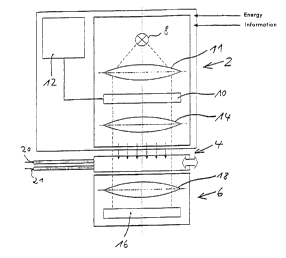
Fig. 1 depicts a first embodiment of an arrangement for
preparing a biochip or/and for manipulating or/and for
studying biologically or biochemically functional
materials immobilized thereon.
The arrangement according to fig. 1 can be conceptually
divided into three groups of functional modules or
system modules 2, 4, 6. The system module 2, also
called below programmable light source matrix, includes
at least one light source 8, at least one illumination
matrix 10 which can be controlled to generate an
optionally adjustable exposure pattern, and a control
computer 12 which may be, for example, a programmable
single chip microprocessor which is able to
communicate, if required, with an external computer via
CA 02341894 2001-02-27
- 33 -
an appropriate interface and which serves to control
the illumination matrix 10 using an appropriate
programme. Alternatively, the illum,~nation matrix can
be controlled from an external computer, for example
personal computer. The system module 2 may further
include optical elements 11, 14 whch may be lenses,
apertures, masks or the like and which are arranged for
possible exchange where appropriate.
The second system module 4 is the exchangeable carrier
or biochip which is to be exposed by the programmable
light source matrix 2. The third system module 6 is a
light detection unit which preferably includes a matrix
made of light sensors 16. The matrix 16 is preferably
an in particular color-capable CCD sensor chip which
can be used for spectrally resolved and intensity
resolved, location-selective measurements. Where
appropriate, the system module 6 may also contain
optical elements 18 such as lenses, apertures, masks or
the like.
The light sensor matrix 16 is arranged opposite and
facing the illumination matrix 10, the carrier 4 being
located in the (transmitted) light path between the
illumination matrix 10 and the light sensor matrix 16.
In the case of the example according to fig. 1, the
illumination matrix 10 is an electronically
controllable optical component whose transparency can
be controlled with spatial resolution according to the
resolution of the matrix, i.e. the arrangement and size
of the matrix elements which form the matrix and which
can be specifically controlled; the transparency can be
switched preferably between two states, namely the
essentially opaque state and a state of maximum
transparency for the light of the light source 8. The
illumination matrix 10 therefore can be considered as
an electronically adjustable mask in a transmitted
light arrangement. Depending on the control by the
CA 02341894 2001-02-27
- 34 -
control computer 12, the illumination matrix 10
generates an exposure pattern which is used for
exposing the carrier 4 location-selectively. The
illumination matrix 10 used in the arrangement
according to fig. 1 is preferably a light valve matrix
(LCD matrix with SPD filling) . It is in principle also
possible to use other light valve arrangements which
can be controlled with spatial resolution, for example
microplates, microsliders, etc., in order to realize an
illumination matrix 10 of the kind depicted in
figure 1.
The detection module 6 may be connected to the computer
12 or, where appropriate, to an external computer, for
example personal computer, to control said module and
to process the measurement information it provides.
The system modules 2 and 6 are preferably arranged on a
shared holder which is not shown in figure 1, and they
can be, where appropriate, adjusted relative to one
another. The holder further has a sliding guide or the
like by means of which the exchangeable carriers 4 can
be introduced in each case into the position according
to figure 1 in a simple manner and can be removed again
from said position for removal of the appropriate
carrier 4.
The arrangement according to figure 1 can be used in
the preferred manner to coat an appropriate carrier 4
location-selectively with biologically or biochemically
functional materials. For this purpose, a carrier 4 is
used which has a surface having photoactivatable
groups. Examples of suitable carriers are i.a. given in
the German patent application 198 39 256.7. The
programmable light source matrix 2 is used to generate
an exposure pattern on the carrier surface provided
with photoactivatable groups, in order to activate the
photoactivatable groups in predetermined areas which
are exposed to the light of the light source 8 in
CA 02341894 2001-02-27
- 35 -
accordance with the exposure pattern. Via the feed 20,
appropriate reagents may be fed to the surface (in the
example to an inner surface of the carrier), which
contain the desired biologically or biochemically
functional materials or building blocks for such
materials which are then able to bind to the
predetermined areas. 21 denotes a discharge tubing for
the reagents.
The biologically or biochemically functional materials
or building blocks may for their part be provided with
photoactivatable groups which can be activated by area
in a possible subsequent activation step in accordance
with the chosen exposure pattern, in order to bind in a
further binding step biologically or biochemically
functional materials or building blocks for such
materials corresponding to the reagents employed. Not
listed above were possible washing steps to flush the
reagents used last, prior to the respective next
exposure step. Depending on the activation wavelength
of the photoactivatable groups, the exchangeable light
source 8 may be a particular radiation source emitting
in the infrared range, in the visible range, in the
ultraviolet range or/and in the X-ray range.
Exposure, washing and binding steps can be repeated in
a specifically controlled manner in order to generate,
for example, a high-density microarray of biomolecules
such as, for example, DNA, RNA or PNA.
Applications of this type do not necessarily require
the light detection module 6; it is, however, possible
to utilize said module expediently for online quality
control of the processes which are light-dependent and
take place in or on the carrier 4, i.e., for example,
for monitoring an in-situ synthesis of biomolecules for
preparing a microarray. The light sensor matrix 16
facilitates monitoring with spatial resolution the
light-dependent processes via optical signals.
CA 02341894 2001-02-27
- 36 -
The light detection module 6 may generally be used for
graduating or calibrating the system prior to a
synthesis or analysis or other reactions or
manipulations on or in the carrier.
The light sensor matrix 16 may, where appropriate, also
be used for type recognition in which, for example, a
carrier or chip body assigned to particular
applications is automatically detected and the
reactions and settings during subsequent processes are
automatically adjusted.
By using the optical elements 14, it is possible to
focus the two-dimensional exposure pattern, where
appropriate, in one or more particular planes in or on
the reaction carrier. Shifting the focusing plane
during a process is also conceivable.
Figure 2 depicts a diagram of a second embodiment of an
arrangement for preparing, studying and/or manipulating
a reaction carrier. Elements in figs. 2 - 6 which
correspond in their function to elements in fig. 1 are
marked with in each case corresponding indicators so
that in this respect the description of the first
exemplary embodiment can be referred to. In the
embodiment according to fig. 2, the illumination matrix
provided for is an electronically controllable
reflection matrix 10a. The electronically controllable
reflection matrix l0a used may be, for example, a high-
resolution surface light modulator with viscoelastic
control layer and mirror layer. Such surface light
modulators with viscoelastic control layers are
illustrated, for example, in the data sheet entitled
"Lichtmodulatoren mit viskoelastischen Steuerschichten"
[Light modulators with viscoelastic control layers]
which has been published by the Fraunhofer Institute
for Microelectronic Circuits and Systems, D 01109
CORRECTED SHEET (RULE 91)
ISA/EP
CA 02341894 2001-02-27
- 37 -
Dresden, Germany (information therefrom on pages 44-47
of the present application). Such a surface light
modulator allows generation of an exposure pattern with
spatial resolution for exposing the ruction carrier.
Alternatively, the electronically controllable
reflection matrix l0a used may also be a surface light
modulator with one or more micromechanical mirror
arrays as is illustrated in the data sheet entitled
"Lichtmodulatoren mit mikromechanischen Spiegelarrays"
[Light modulators with micromechanical mirror arrays)
which has been published by the Fraunhofer Institute
for Microelectronic Circuits and Systems (information
therefrom on pages 48-52 of the present application).
Reflection surface light modulators have also been
developed by Texas Instruments.
Very generally, such electronically controllable mirror
matrices with CMOS 40V technology are very well suited
to the requirements of the present invention, since
they can be employed over a broad spectral range, in
particular also in the UV range in order to generate
the desired exposure patterns. This is not true for W
sensitive mirror matrices with, for example, 5V
technology.
Direction of the light path according to fig. 2
additionally requires a light deflection element 24
which may be, for example, a partly transparent mirror
which deflects the light coming from the light source 8
to the reflection matrix l0a and allows the light which
is reflected back from the reflection matrix l0a to
pass through downward to the reaction carrier 4 so that
it is possible to utilize on the reaction carrier 4 or,
where appropriate, in the reaction carrier 4 the
exposure pattern generated in accordance with the
control of the reflection matrix l0a for
CORRECTED SHEET (RULE 91)
ISA/EP
CA 02341894 2001-02-27
- 38 -
photoactivating, analyzing or manipulating biochemical
processes.
Fig. 3 shows a variation of the embodiment according to
fig. 2, in which the embodiment of fig. 3 has a light
path for which the deflection element denoted as 24 in
fig. 2 can be dispensed with, since the controllable
reflection matrix l0a is arranged such that it can
deflect light coming from the light source 8 to the
reaction carrier 4 in accordance with the chosen
exposure pattern. When using a structure corresponding
to the variation of fig. 3, the image of a carrier with
meandering channel is visible in fig. 13. In this case,
there are no optical elements whatsoever between
carrier and CCD sensor, so this is a lens-less direct
detection. The light source used in this case is a
laser.
Fig. 4 depicts a diagram of another embodiment of an
arrangement for preparing, studying or/and manipulating
a carrier of the present invention. In the embodiment
according to fig. 4, the illumination matrix used is a
matrix arrangement lOb made of light sources, for
example a microlaser array or a microdiode array. At
the moment developments are taking place which are
aimed at putting a multiplicity of microscopically
small semiconductor lasers as tiny powerful light
sources on a single chip. A controllable "light chip"
of this type could be used as matrix lOb. Regarding
literature on the background of the "light chips", the
journals: Nature 3, 97, pp. 294-295, 1999 and MPG-
Spiegel 4/98, pp. 13-17 may be referred to for example.
Fig. 5 shows an arrangement in which the detection
module 6 with sensor matrix 16 ;~s set up for reflected
light or backlight observation of the reaction carrier
4.
CORRECTED SHEET (RULE 91)
ISA/EP
CA 02341894 2001-02-27
- 39 -
All arrangements according to figures 1-5 can be used
as light-emission detectors for detecting the optical
behavior of a carrier test area provided with
biologically or biochemically functional materials.
This may take place in a manner as is disclosed in the
German patent application 198 39 254Ø
Fig. 6 shows a section through an embodiment of a
carrier 4 of the invention, said embodiment being
distinguished by the illumination matrix 10 being part
of the carrier body 4. In this case, the illumination
matrix used is preferably a light valve matrix which
can be disposed of together with its chip carrier 4,
after the carrier is no longer used.
In the exemplary case of fig. 6, the carrier body 4 has
capillary channels 30 whose walls serve as preparation
surface for the coating with biologically or
biochemically functional materials. The channels 30 can
be selectively charged with the appropriate reagents.
The following details are detectable in fig. 6:
boundary layers 32 with transparent and nontransparent
areas 34 and 35, respectively, transparent electrodes
36 with SPD particles (suspended particles) enclosed
between and to be influenced by the electrodes 36, or
alternatively liquid crystals 38.
Figure 7 depicts a greatly simplified diagram of a
light-emission detector of the invention in the form of
a sandwich structure composed of light valve matrix 103
(two-dimensional liquid crystal exposure element),
transparent sample carrier 105 with sample material 107
included therein and CCD matrix 109 (image recorder).
The light valve matrix 103 and CCD matrix 109 can be
controlled from a shared (not shown) control unit, for
example in order to switch matrix elements of the light
CORRECTED SHEET (RULE 91)
ISA/EP
CA 02341894 2001-02-27
- 40 -
valve matrix and the CCD matrix assigned to one another
into the active state simultaneously.
The arrangement shown is suitable, for example, for
measuring the optical absorption of the sample material
107 in the transparent carrier 105. The sample material
107 may be microparticles (smart beads), for example.
Such an arrangement is shown in fig. 12. Here, a
commercially available Neubauer cell counting chamber
as transparent carrier 105 has been filled with colored
microparticles 107. When illuminating with a light
source 8, consisting of a cold light source with fiber
coupling-out and aperture (802), colored microparticles
can be detected by the CCD sensor and the color can be
determined by absorption (not visible in black and
white). After labeling the microparticles with
fluorophores, it is possible to detect said
fluorophores in the same way by the CCDs sensor using a
suitable light source.
Means for positioning the light valve matrix relative
to the CCD matrix are not visible in fig. 7. Said means
could be, for example, means for tilting the light
valve matrix 103 relative to the CCD matrix 109. Of
course, it is possible to choose numerous other
possibilities in order to position the light valve
matrix 103 and the CCD matrix 109 in the correct
position to one another and, where appropriate, to fix
them to one another.
Fig. 8 shows another arrangement for the spatially
resolved photochemical synthesis of polymer probes on a
carrier and/or for manipulating and/or studying
immobilized, biological, biochemically functional
materials. The arrangement according to Fig. 8 can be
conceptually divided into the three functional modules
201, 203 and 206. In this connection, the system module
CORRECTED SHEET (RULE 91)
ISA/EP
CA 02341894 2001-02-27
- 41 -
201 constitutes an illumination matrix, for example in
the form of an LED matrix, which in a software-
controlled manner generates an illumination pattern
which can induce the spatially resolved photochemical
synthesis of polymer probes in the carrier 203.
Coupling the illumination pattern in the carrier 203 is
carried out with the aid of the system component 202.
Said system component may be, for example, a mechanical
mask with an aperture for each LED matrix element. More
suitable is the use of micro-optical elements such as
microlenses, for example. Furthermore, said system
component may also be a fused fiber optical taper which
makes it possible to considerably reduce divergence of
the light emitted from the individual light source
elements. Opposite the carrier 203, an optical four-
channel detector (preferably a CCD sensor or a CCD
camera) is located on the exit side of the light. The
working mode of said CCD camera is adjusted to the
operation of the illumination matrix 201 with the aid
of suitable hardware or software. For controlling,
preference is given to using a personal computer which
controls the illumination matrix and the CCD camera.
Alternatively or additionally, a frequency generator
may also be used for controlling and for electronically
synchronizing the illumination matrix 201 and the, in
this case,,gated CCD chip 206 with one another. The
latter embodiment will facilitate in particular
fluorimetric detection of the analytes bound to the
carrier 203 without it being necessary to introduce
additional frequency-selective elements between the
carrier 203 and the detector matrix 206. However, as
has already been mentioned above, a precondition for
this method is to be able to swi~ch the individual
elements of the illumination matrix on or off within a
time range of a few nanoseconds. An alternative to this
is an optical filter 204 which can facilitate spectral
separation of the exciting light ar_d the signal light
CORRECTED SHEET (RULE 91)
ISA/EP
CA 02341894 2001-02-27
- 42 -
in fluorimetric detection. When using a filter wheel
204, it is moreover possible to analyze simultaneously
on the same carrier 203 analytes of different sample
materials which have been labeled with fluorophores of
distinctly different emission maxima. The location
selective reproduction of the signal light emitted from
the carrier 203 on the detector matrix 206 may
optionally be carried out using the component 205. Said
component may either be an optical lens system or a
fused fiber optic taper.
Figures 9, 10 and 11 show further possible embodiments
of a device of the invention. Common to all these
embodiments is the reproduction of the illumination
pattern generated by the illumination matrix 201 on the
carrier 203 at a reduced size. Elements in figures 9,
10 and 11 which correspond to the elements in fig. 8
with respect to their function, are marked by in each
case corresponding reference symbols so that in this
matter the description of the exemplary embodiment
according to Fig. 8 may be referred to. For the
embodiment according to fig. 9, the optical image is
reduced by guiding the beam in a fused fiber optic
taper 207, whereas in the exemplary embodiment
according to fig. 10 reduction is achieved using a
suitable optical lens system 208. Both micro- and
macrolens systems may be employed here. The exemplary
embodiment depicted in fig. 11 finally uses a
combination of a fused fiber optic taper 207 and an
optical lens system 208.
In summary, the following should also be noted
regarding figures 8 - 11. They show a device having a
light source matrix, a micro-optical component and also
reducing optics for light-controlled induction of
spatially resolved chemical or biochemical syntheses in
one reaction carrier. In the case of using an LED
CORRECTED SHEET (RULE 91)
ISA/EP
CA 02341894 2001-02-27
- 43 -
matrix as light source matrix, it has proved to be
expedient, that no more than 75% of the light source
matrix surface area is covered with LEDs.
It should be mentioned that one or more gaps between
individual elements of the device may be filled with an
optical fluid.
With respect to the inventive embodiment depicted in
figure 3, figure 12 shows an arrangement including a
transparent carrier 105, for example a commercially
available Neubauer cell cell chamber which has been
filled with colored microparticles 107. When
illuminating with a light source 8, for example a cold
light source with fiber coupling-out and aperture
(802), the colored microparticles can be detected by
the CCD sensor matrix (16) and the color can be
determined by absorption. When labeling the
microparticles with fluorophores, detection by the CCD
sensor can be carried out in an analogous manner.
Figs. 14 and 15 were taken from the data sheets:
"Lichtmodulatoren mit viskoelastischen Steuerschichten"
[Light modulators with viscoelastic control layers] and
"Lichtmodulatoren mit mikromechanischen Spiegelarrays"
[Light modulators with micromechanical mirror arrays]
of the Fraunhofer Institute for Microelectronic
Circuits and Systems, IMS 1998 (therein in each case
fig. 1) .
CORRECTED SHEET (RULE 91)
ISA/EP
CA 02341894 2001-02-27
- 44 -
Information from the data sheet:
"Lichtmodulatoren mit viskoelastischen Steuerschichten"
[Light modulators with viscoelastic control layers]
by the Fraunhofer Institute for Microelectronic
Circuits and Systems, IMS, D-01109 Dresden, Germany
Features
Viscoelastic control layers form a class of high-
resolution surface light modulators (SLMs) with
deformable mirror arrangements. Trey consist of an
array of independently controllable control electrodes
on an underlying active CMOS control matrix which is
coated with a viscoelastic silicone gel. A thin
aluminum layer is applied thereupon which forms a
continuous mirror surface and has h-gh reflectivity in
the complete range from IR to far UV.
Operation principle
Fig.l (depicted in fig. l4 of the present application)
shows diagrammatically the cross section of a
viscoelastic control layer. To activate, a bias is
applied between the mirror and the control electrodes
which puts the arrangement in its entire area under
mechanical pressure. The surface initially stays smooth
and acts optically as a planar mirror. Only application
of an additional control voltage with alternating
polarity to neighboring control electrodes leads to a
deformation owing to the changing electrical field
strengths. Switching the polarity either for one or
both spatial directions can genera~e either 1D or 2D
sinusoidal deformation profiles.
Fig. 2 (of the IMS data sheet) shows in this connection
CORRECTED SHEET (RULE 91)
ISA/EP
CA 02341894 2001-02-27
- 45 -
the surface profiles measured for an embossed-engraved
pattern. Optically, these deformation profiles are
phase grids whose grid period is defined by the
distance between the control electrodes. The incoming
light undergoes a phase modulation corresponding to the
differences in the optical path given by the mirror
deformation. Choosing an appropriate deformation
amplitude makes it possible to deflect nearly the
entire amount of light into higher orders of
deflection, whereas the light of non-addressed planar
pixels only occupies the zero order.
In connection with a suitable optical system, it is
then possible to achieve the situation where only light
of non-addressed areas is let through and is projected
into the focal plane as visible intensity pattern.
Viscoelastic control layers are therefore well suited
to generating phase patterns for optical imaging
applications. Using this technology, an SLM prototype
working in binary mode with an active matrix of 1024 x
2048 pixels and 20 x 20 ~.m2 pixel size was developed,
with a specific high-voltage CMOS process being
employed to facilitate control voltages of up to ~15 V.
Fig. 3 (of .the IMS data sheet) shows in this connection
the diagrammatic layout of the active control matrix.
The operation of this prototype was successfully
demonstrated in an application for fast direct laser
exposure of sub-~C structures. Said prototype served to
generate phase patterns from the CAD layout data of IC
mask layers, which patterns were then converted into an
intensity image for the photoresist structuring with
the aid of the optical system.
At present, light modulators are being developed which
allow 4-bit analog operation and graduation of the
CORRECTED SHEET (RULE 91)
ISA/EP
CA 02341894 2001-02-27
- 46 -
image field size in steps of 255 pixels for each
direction.
Applications
Light modulators with viscoelastic control layers open
up many new application possibilities:
Display technology:
- Video and data projection
- Head-up displays
Information technology:
- Optical image and data processing
- Optical storage
Production technology:
- Mask-free direct writing
- Laser ablation and production
Technical parameters
Pixel size > 16 x 16 ~m2
Pixel number 256 x 256 ... 1024 x 2048
Profile 1D, 2D sinusoidal
Modulation phase-modulating
Operation binary or 4-bit analog
Deformation amplitude 0 ... 150 nm
Control graph nearly linear
Adjustment time < 2 ms
Data inputs 16, 32, 48, 64 channels
4 bit, 5 V
Image frequency 100 Hz ... 500 Hz
Optical filling 100%
Reflectivity > 90% IR ... DUV) far UV
Construction technology ceramic PGA shell
CORRECTED SHEET (RULE 91)
ISA/EP
CA 02341894 2001-02-27
- 47 -
User Evaluation Kit
In order to provide the possibility of testing all
fundamental SLM functions in a user-specific
environment, a user evaluation kit containing all
components for user-specific image programming of the
SLMs was developed.
SLM
Pixel size 16 x 16, 20 x 20, 24 x 24 ~.m2
Pixel number 256 (160) x 256
Pixel design customer-specific
Operation 4-bit analog
SLM board
g~ Storage of 2 images
Image frequency 1 Hz (PC to RAM)
500 Hz (RAM to SLM)
I/O signals Matrix Trigger, Matrix Ready
Data transfer
- via cable connection and digital I/0 interface
card for ISA slot on the PC
Software
Conversion of user image data from bitmap into SLM
data format
- Control functions for data transfer
- Setting the control voltage level for 4-bit
grayscale
Requirements
CORRECTED SHEET (RULE 91)
ISA/EP
CA 02341894 2001-02-27
- 48 -
- Windows-compatible PC
- Image pattern generation in b=tmap data format,
for example using Paintbrush
Information from the data sheet:
"Lichtmodulatoren mit mikromechanischen Spiegelarrays"
[Light modulators with micromechanical mirror arrays]
by the Fraunhofer Institute for Microelectronic
Circuits and Systems, IMS, D-01109 Dresden, Germany
Features
Micromechanical mirror arrays form a class of high-
resolution surface light modulators (SLMs) with
deformable mirror arrangements. They consist of an
array of independently contollable micromirrors which
are produced on an underlying active matrix control
circuit in a completely CMOS-compatible process using
the methods of surface micromechanics. The process only
needs three additional masks and thus allow easy
adaptation of the light-modulating properties to a wide
variety of application-specific requirements by merely
changing the mirror architecture.
Operation principle
The micromirrors are produced using a sacrificial layer
technique, so that hanging mirror elements are created
above a cavity with underlying control electrode.
Mirror and supporting beams consist to the same extent
of aluminum in order to guarantee high reflectivity
over a broad spectral range from IR to far UV.
CORRECTED SHEET (RULE 91)
ISA/EP
CA 02341894 2001-02-27
- 49 -
Activation takes place by applying a control voltage
between mirror and control electrode so that the
mirrors are deformed into the cavity due to the action
of electrostatic forces. The differences in the optical
path related thereto lead to a corresponding phase
modulation in the incoming light. The deformation
profile and thus the light-modulating properties depend
in this context strongly on the particular mirror
architecture. Here, three fundamental cases, phase-
modulating, phase-shifting and light-deflecting, can be
distinguished.
From the multiplicity of possible pixel architectures,
the two structures from fig. 1 (depicted in fig. 15 of
the present application) have been studied in more
detail.
In the first variation, electronic deformation of four
identical mirror segments generates optical phase grids
in which one pixel defines in each case one grid period
with inverse pyramidal phase profile. Said variation is
well suited to generate phase patterns for optical
imaging applications.
The second variation consists of a mirror plate held by
four arms, which mirror plate delivers, when
electronically controlled, a planar piston-like
descending movement and thus allows setting the phase
of the incoming light for each pixel. This variation is
well suited to phase front correction in adaptive
optics.
Such micromirrors have already been built on passive
matrices for studying the electromechanical properties
( fig . 2 , 3 of the IMS data sheet ) . The measured graphs
in fig. 4 (of the IMS data sheet) show in this
connection the typical deformation behavior. In the
CORRECTED SHEET (RULE 91)
ISA/EP
CA 02341894 2001-02-27
- 50 -
analog field, deformation increases almost quadratic
with the control voltage. Above the so-called pull-in
point the mirrors, however, owing to the co-coupling
via the electric field, switch spontaneously to the
fully extended state in which only binary operation is
still possible. In order to ser the mirrors finally
back to an equilibrium between mechanical and
electrical powers, an appropriate reduction of the
control voltage is necessary.
Applications
Light modulators with micromechanical mirrors open up a
multiplicity of application possibilities:
Display technology:
- Video and data projection
- Head-up displays
Information technology:
- Optical image and data processing
- Optical storage
Phase front correction of adaptive optics
Production technology:
- Mask-free direct writing
- Laser ablation and production
Medical technology:
- Laser scanning tomography
- Laser surgery
- Endoscopic head-up displays
Technical parameters
Pixel size > 16 x 16 um2
CORRECTED SHEET (RULE 91)
ISA/EP
CA 02341894 2001-02-27
- 51 -
Pixel number 256 x 256 ... 1024 x 2048
Pixel design customer-specific, pyramidal,
descending, torsion elements,
Profile etc., pyramidal, rectangular,
sawtooth, etc.
Modulation phase-modulating or -shifting,
deflecting
Operation binary or 4-bit analog
Deformation amplitude 0 ... 1.2 um (analog) up to 5.0
~m (binary)
Control graph nonlinear
Adjustment time 10 ~.s (typ. )
Image frequency 100 Hz ... 1 kHz
Optical filling 80 ... 90%
Reflectivity > 90% (IR ... DUV) far W
User Evaluation Kit
In order to provide the possibility of testing all
fundamental SLM functions in a user-specific
environment, a user evaluation kit containing all
components for user-specific image programming of the
SLMs was developed.
SLM
Pixel size 16 x 16, 20 x 20, 24 x 24 ~Cmz
Pixel number 256 (160) x 256
Pixel design customer-specific
Operation 4-bit analog
SLM board
RAM Storage of 4 images
Image frequency 1 Hz (PC to RAM)
500 Hz (RAM to SLM)
CORRECTED SHEET (RULE 91)
ISA/EP
CA 02341894 2001-02-27
- 52 -
I/0 signals Matrix Trigger, Matrix Ready
Data transfer
- via cable connection and digital I/O interface
card for ISA slot on the PC
Software
Conversion of user image data from bitmap into SLM
data format
- Control functions for data transfer
- Setting the control voltage level for 4-bit
grayscale
Requirements
- Windows-compatible PC
- Image pattern generation in bitmap data format,
for example using Paintbrush
CORRECTED SHEET (RULE 91)
ISA/EP