Note: Descriptions are shown in the official language in which they were submitted.
CA 02342101 2006-04-11
20365-4367
Optical amplifiers and optical transmission path
The invention relates to controlled optical
amplifiers and optical transmission paths in which these
amplifiers are used.
Optical amplifiers are used in optical
transmission networks to compensate for fiber attenuation.
However, stable operation over additional transmission paths
is possible only if changes to system parameters are
compensated with the aid of controllers. In previously used
wavelength division multiplex transmission systems, the sum
output powers of the amplifiers are controlled. In single-
channel systems or paths with a constant number of channels,
slow changes to system parameters - for example due to
temperature fluctuation or aging - are effectively
compensated by this control concept.
A device to amplify an optical WDM signal by means
of an optical fiber (e.g. EDFA) is described in the document
"Patent Abstract of Japan, JP-A-05063643". The amplifier
has two photoelectric elements which measure the light power
upstream and downstream of the amplifier. The power of the
pump source is controlled by the difference between the two
photoelectric signals in relation to a defined reference
voltage in such a way that the amplification of the
amplifier is adapted to a specific value.
An optical transmission system with an improved
signal-to-noise ratio is described in the document "United
States Patent, US-A-5446812". A plurality of amplifiers are
connected in succession via the transmission path and are
selectively controlled, either statically or dynamically, by
a control unit in such a way that the maximum signal-to-
1
CA 02342101 2006-04-11
20365-4367
noise ratio or OSNR is obtained at the output of the
transmission path.
A transmission system with successively connected
amplifiers is described in the document "Patent Abstract of
Japan, JP-A-04293025". As in the document "United States
Patent, US-A-5446812", a control signal is fed to all
amplifiers for gain control. According to the Abstract, a
varying pilot signal is used as a reference signal to set
the amplification.
None of the aforementioned three systems enables
the power per channel to be maintained at a constant level
with different numbers of channels.
However, if the number of channels changes during
operation, a sum output power control of this type modifies
the levels of the individual WDM transmission channels. A
level change of this type can essentially be avoided by
determining the number of active channels and informing the
control devices of the individual optical amplifiers. These
accordingly adapt the required value for the output level of
the amplifier. However, due to the different time
constants, this level adaptation does not normally succeed
without transient fluctuations, which are associated with
substantial transmission quality losses.
A different possible solution comprises the
control of the individual amplifiers for constant gain
(amplification). Amplifiers of this type are described in
"Electronic Letters", 26th March, 1991, Vol. 27, no. 7,
p 560-561 and "Electronic Letters", 9th June, 1994, Vol. 30,
no. 12, p 962-964. In these circuits, if the number of
active channels changes, the level fluctuations of the
remaining channels are suppressed by holding the gain
2
CA 02342101 2006-05-29
20365-4367
constant. However, this control principle is also
unsuitable as a control concept for a transmission path with
a plurality of amplifiers, since slow changes in the path
parameters are added together, resulting in a deterioration
in transmission quality.
Embodiments of the invention therefore provide
suitable amplifiers for optical transmission networks.
Furthermore, the transmission paths are to be designed in
such a way that, even if the number of channels changes, the
reception levels of the individual WDM channels remain
constant.
Accordingly, in one aspect of the present
invention, there is provided a regulated optical amplifier
for wavelength-division multiplex signal transmission,
comprising: a first control device for regulating the gain;
and a second, dominating control device having significantly
slower control behavior for regulating an output power
according to a supplied reference input.
Transmission paths equipped with these amplifiers
are provided in further aspects. In another aspect of the
invention, a transmission path is characterized in that the
rated value determining a respectively desired output power
is supplied to the optical amplifiers as the reference
input.
Advantageous further developments are described
herein.
The advantage of the optical amplifier according
to the invention lies in that the gain control operates in
the first control circuit with a short time constant.
Changes in the number of active WDM channels therefore have
only a minimal effect on the output levels. The second
3
CA 02342101 2006-05-29
20365-4367
control circuit ensures that slow changes are compensated.
If the number of active channels changes, a corresponding
change in the required value of the second control circuit
is carried out by means of a terminal (network node), either
3a
CA 02342101 2006-04-11
20365-4367
at the transmitting end, inserted locally in the
transmission path or at the receiving end, so that the
output level control - if provided - is perceptible for only
a short time and to only a minimal extent.
If a memory unit is provided in the second control
circuit, it is thus possible to allow this control circuit
to be active only at specific times in order to modify the
reception level or de-activate it during a change in the
number of channels.
In the alternative solution, the output power is
controlled either jointly for all amplifiers of one
transmission path from the reception terminal or, with
corresponding, individual monitoring of the output levels,
also separately via a correspondingly designed monitoring
channel.
Through the use of an output level control, the
amplifiers only require information on the number of WDM
channels, or receive a corresponding required value.
The transmission paths equipped with those
amplifiers can also compensate for slow amplification
changes caused by aging processes.
The invention is described in more detail with
reference to two embodiments, wherein:
Figure 1 shows a basic circuit diagram of the
amplifier according to the invention with output power
control,
Figure 2 shows a basic circuit diagram with an
optical fiber amplifier,
4
CA 02342101 2006-04-11
20365-4367
Figure 3 shows a transmission path with a
plurality of amplifiers,
Figure 4 shows a variant of the amplifier
according to the invention, and
Figure 5 shows the use of this amplifier on a
transmission path.
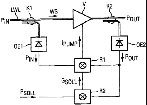
An embodiment of the invention is shown as a basic
circuit diagram in Figure 1. An optical amplifier V serves
to amplify a wavelength division multiplex signal MS which
is transmitted via an optical waveguide LWL. At the input
side, a first measurement coupler Kl is provided, which taps
part of the signal. This part is converted by a first opto-
electronic transducer OE1 into an electrical measurement
signal PIN corresponding to the input level (input sum power)
PIN, which is fed to a first controller R1. Similarly, a
measurement signal pouT, which corresponds to the output
power POUT and which is likewise fed to the first controller,
is obtained via a second measurement coupler K2 and a second
opto-electronic transducer 0E2. Depending on the
(adjustable ratio) POUT to PIN, for example, the pump current
IPUMP in an optical-fiber amplifier or the control current in
a semiconductor amplifier is controlled. Other gain control
principles can equally be applied, which, for example, are
described in the cited literature.
Apart from a first control device (control
circuit, shown in simplified form) (K1, OE1, K2, 0E2, Rl, V)
which is used for fast gain control, a second dominant
control device (control circuit K2, 0E2, R2, Rl, V) is
provided, which controls the output power (output level) POUT
through comparison of the corresponding measurement value
POUT with a feed parameter, the required value psoLL. Slow
5
CA 02342101 2006-04-11
20365-4367
changes in transmission loss, caused, for example, by a
change in temperature or aging, are compensated by this
second control circuit. By acting on the first control
circuit, the setting parameter GSOLL output by the second
controller R2 determines the pump current and therefore the
gain of the optical amplifier. If the number of
transmission channels changes, the gain should not change.
The level control must not therefore become immediately
active, which can be achieved by means of a time constant of
the second control circuit which is normally very much
greater than the time constant of the first control circuit.
Figure 2 shows details of the amplifier circuit
with an optical fiber amplifier VFA, whose gain is
determined by the pump current Ipuyp generated by a controlled
pump laser PL, said current being injected via a pump
coupler PK. The first controller Rl may contain an
attenuator DG, which is connected to the second opto-
electrical transducer 0E2 and a first comparator COM1. If
the second control circuit is left out, the gain can be
adjusted with the attenuator. One possibility for "output
level control through gain modification" would involve
direct modification of the attenuator DG by means of the
feed parameter PsoLL=
In the embodiment, the comparison between the
output level and the feed parameter PSOLL takes place in the
second control device (in the second control circuit) K2,
0E2, COM2, MU, IN, COM1, PL, PK, VFA - as already described
in principle in a second comparator COM2. Via the
multiplier MU, the result of this comparison modifies the
input signal of the first comparator COM1 and in this way
controls the pump current and therefore the gain of the
optical fiber amplifier VFA. The attenuator can be
6
CA 02342101 2006-04-11
20365-4367
dispensed with, since the second control circuit determines
the gain via the multiplier.
As already mentioned, the time constant in the
second control circuit should be adequately large so that,
in the event of the change in the number of channels, it can
neutralize the effect thereof by means of a corresponding
externally performed modification of the feed parameter. A
memory unit SH may also be helpful for this purpose. This
can also be inserted between the integrator and the
multiplier. A range of around 1 microsecond to one
millisecond is adequate as a time constant for the first
control circuit at high data rates in the megabit/second
range, whereas a range of around 0.1 second to several
seconds, minutes and hours is appropriate for the second
control circuit. The time constant can also be switched
over for different operating conditions.
A small time constant of, for example, 100
microseconds can therefore be selected for commissioning,
whereas, in the event of a change in the number of channels,
a time constant of 1 sec and, if a required level
modification is carried out, a time constant of several
minutes may be appropriate.
An integral action or at least an integral
component, which can also be supplemented by a dead time, is
suitable for the second controller. The second comparator
and the integrator can be combined in a circuit design.
The amplifier circuits with the associated control
circuits may of course be designed in any required manner.
Figure 3 shows a transmission path with a
plurality of optical amplifiers VT, Vi to Vn. In a
transmission terminal Tl, a wavelength division multiplex
7
CA 02342101 2006-04-11
,20365-4367
signal MS is generated in a transmission device TR with a
downstream wavelength division multiplexer WDM, is amplified
in an optical amplifier VT and inserted into the path. The
amplifiers are set in such a way that they deliver output
levels which correspond to the conditions of the relevant
path section and which are maintained by the second control
circuit even in the event of slowly changing transmission
characteristics.
If the number of WDM channels changes, the output
level initially continues to be held constant in each
channel by means of the first control circuit. Due to the
slow time constant/dead time, the output level controller
does not initially act on the control process. Since the
change in the feed parameter which serves to set the new
output level is simultaneously signaled via a monitoring
channel OCH from the terminal to the amplifiers, the second
control circuit has virtually no effect. Separate channel
number monitoring, which is allocated to each amplifier is,
on the other hand, still too expensive.
It must also be noted that the output powers may
also be individually adjustable via the monitoring channel.
Figure 4 shows a variant VV of the amplifier
according to the invention. The second control device for
direct control of the output level is missing. The gain can
be set only via the monitoring channel OCH in order to be
then held constant by the first control circuit. Thus, an
external modification of the output level is in turn also
possible. In this example the setting is determined via a
digital/analog converter DAW, whose output signal as a
control signal GSOLL determines the gain.
8
CA 02342101 2006-04-11
.20365-4367
Figure 5 shows a further transmission path with
optical amplifiers VV1 to VVn, in which this amplifier type
can be advantageously used. A terminal T2 at the receiving
end contains not only an amplifier VVn and a wavelength
demultiplexer WDD, but also a receiving device RE, which
determines the sum level and the number of active WDM
channels. From the second terminal, the numbers of channels
or corresponding required values are indicated via the
transmission channel OCH to the amplifiers and, in the event
of system-related slow changes in the reception level, the
extent to which the gain of the individual amplifiers is
modified is also established. The second "control circuit"
is thus always formed via the reception terminal. In simple
embodiments of the setting device and amplifiers, the same
gain modifications can be made for all amplifiers and, in
more expensive designs, individual modifications can be made
to individual amplifiers according to the path parameters or
according to monitoring devices. By means of
correspondingly designed controllers, the output levels can
also be defined directly or modified in relation to
predefined levels.
9