Note: Descriptions are shown in the official language in which they were submitted.
CA 02342155 2000-12-18
LINEAR TRAVELING WAVE TUBE .a~'~iPLIFIER
UTILIZING INPUT DRIVE LIMITER FOR OPTIMIZATION
BACKGROUND OF THE INVENTION
I. Field of the Invention
The present invention relates to systems and methods of amplifying signals and
in
particular to a system and method for limiting the average power output of a
traveling
wave tube amplifier without limiting peak power output.
I 0 '_'. Description of the Related An
Combining a linearizer with a traveling wave tube amplifier I T~VT) allows for
more efficient operation of the power amplifier while maintaining linear
performance. To
fully exploit this advantage it is desirable to optimize the TWT for best
efficiency at the
operating point. For most ~r~VT designs. optimizing for efficiency at a backed
off
I,~ operating point results in a condition where increasing drive levels above
the operating
point can be damaging to the T~VT due to collector backstreaming and beam
defocusing
problems. Designing the r~VT to handle the higher drive levels also results in
increased
cost and design complexity.
One possible way oh~ protecting the fW'T i~ to incorporate an input drive
limner
=0 into the lincarizer. l ~ntortunatelv, limitinsr the drive Imel is not
compatible with linear
CA 02342155 2000-12-18
rertormance of the system. 1-o provide linear performance under multicarrier
operation.
an amplifier must have an amplitude modulation-to-amplitude modulation tAM-AMl
transfer characteristic that is linear for a range of drive levels above and
below the
operating point. This requirement is due to the way that the multiple carriers
sum together
~ resulting in high peak powers. For example. for two equal carriers, the peak
power is 6
dB above the average individual carriers. For multiple carriers. the peak
value can be
much higher. that is. approximately 8.4 dB for 8 carriers randomly phased. Any
limner
would have to be set at a level that is 6 or more dB higher than the operating
point and
this would eliminate almost all advantages of optimizing the TWT at back-off.
I 0 Another way of protecting the TWT is to use limiters that limit both peak
as well
as average power. These are implemented using a simple saturating amplifier.
Such
limners afford some protection to the TWT but in order to preserve linear
performance.
they must be set at a point that is tar above the required operating point.
This greatly
limits their value in this application. This type of limner is typically set
at a saturation
15 point of the TWT or higher and only provides protection from accidental
overdrive
conditions.
Although circuits for compensating the gain compression and phase of nonlinear
amplifiers such as traveling wave tubes exist in the prior art. none of these
circuits
include a limner that limits average power without limiting peak power as
well. For
~0 example. although U.S. Patent No. x.304.944. issued to Copeland et al.
discloses a
passive limner made up of PIN diodes. this n~pe of limner will not achieve the
result of
the present invention as it will limit peak power as well as average and
therefore will
degrade linearity if set near the desired operating point. U.S. Patent No.
5.598.127, issued
to Abbiati et al.. discloses a procedure and circuit for adjusting the
compensation of gain
~5 distortions in a microwave amplifier. -the procedure is based on a circuit
that monitors the
ratio of peak to average power and feeds back a signal to adjust the
compensation circuit
before the amplifier. and in which the control circuit is adjusted such that
the peak to
average power ratio ot~the output remains constant. fl~is control circuit
provides a means
for maintaining linear performance in the presence ot~changine amplifier
linearity due to
;0 life or environmental chanLes. but provides no me:Irts of protection for
the high power
CA 02342155 2000-12-18
amplifier because the average power is not controlled and could increase
beyond the
capability of the amplifier. Also. this circuit relies on monitoring the
output power of the
amplifier. which adds complexiri~ and loss to high power systems.
W hat is needed is a system and method that allows optimizing a linearized
traveling wave tube amplifier for both linearity and efficiency at the
operating point while
protecting the TWT from inadvertent excursions of input drive levels. The
present
invention satisfies that need.
SUMMARY OF THE INVENTION
.~s noted above, an optimized TWT design must provide linearity. vet protect
the
TWT from inadvertent drive level excursions at the same time. The resolution
of these
apparently incompatible design goals is problem is rooted in the discovery
that TWT
failure modes and TWT linearity are influenced by distinctly different signal
and power
dynamics. The present invention advantageously uses a measure of these signal
dynamics
advantage to provide both TWT linearity and resistance to damage from
excessive drive
level.
Signal peaks encountered during multicarrier operation exist only for short
periods
of time and are not damaging to the TWT. The difference between peak and
average
power becomes more pronounced (and in a predictable manner) as the number of
carriers
~0 increases. Operating the TWT under multicarrier conditions will not produce
damage
provided that the average power is not increased above the optimized operating
point.
However. the TWT can be damaged by excessive average power levels. These
excessive levels generally occur under accidental conditions in test or in
operation due to
changes in attenuation such as changes in atmospheric attenuation of the
uplink signal.
'_'S In accordance with the foregoing. the present invention discloses system
comprising an average power dependent attenuator and a TWT~\. if required a
predistortion linearizer can be added to further improve linearity. :\n
attenuator that has a
slow frequency response such that peak powers are passed with minimal
attenuation but
averaLe powers are subject to a large attenuatiun is positioned betorc thc:
radio frequency
~0 i RFl input of the fW'T:\. fhe result is a system that has an :\Vt-.-W1
transfer
CA 02342155 2000-12-18
characteristic that is dependent on average power. Fur low average power the
transfer
curve is linear to drive levels tar in excess of the required operating point.
If the averaee
power is increased to levels above the required operating point the input
attenuation
changes and the transfer curve shifts to a lower output power but retains its
shape. In this
way an averaee output power is maintained that drives the T~VTA at the desired
operating
point and no higher.
The implementation of the average power limner can be accomplished by a
voltage controlled attenuator circuit which is driven by a detector circuit
that produces a
substantially non-alternating or direct current ( DC) voltage proportional to
average'
power.
In accordance with the foregoine. the present invention discloses a method and
apparatus for limiting an average power output of an amplifier without
limiting the peak
power output of the amplifier.
The method comprises the steps of dynamically determining a value proportional
to an average power of an amplifier input signal and substantially independent
from a
peak power of the amplifier input signal. dynamically attenuating the
amplifier input
signal according to the value. and applying the dynamically attenuated
amplifier input
signal to an amplifier to produce the amplifier output signal.
The apparatus comprises a detector for dynamically producing a detector signal
~0 proportional to an average power of the input signal and substantially
independent from a
peak power of the input signal. and an attenuator in communication with the
detector and
the amplifier. for dynamically attenuating the input signal according to the
detector signal.
In one embodiment. the detector comprises a current rectifier such as a diode
device in series with a low pass filter. which can be implemented by a simple
resistive-
~5 capacitive (RC) circuit. In another embodiment. the attenuator comprises a
shunt limner
such an enhancement rigid effect transistor ( FET) with a care coupled to the
detector.
The foregoing implements an average power limner that prevents a TWT from
uperaung at output powers higher than the required operating point. ~mploving
this
limner allows for the fV'Ts to be optimized for performance at the required
operating
'0 point. resulting in higher ~tticicncv and eliminates the need to size the
;amplifier for a
CA 02342155 2004-02-12
power level any larger than the required operating point which
reduces the cost and complexity of the system. The power
limiter protects the TWT while not degrading the linear
performance of the TWT by limiting the average power while
5 allowing peak powers of short duration to pass with low loss.
This provides an optimized traveling wave tube amplifier
optimi2ed for both linearity and efficiency at the operating
point while protecting the TWT from inadvertent excursions of
input drive levels. The present invention is especially
to applicable to high power microwave amplifier systems
specifically including systems that operate with multi-carrier
signals.
In accordance with another aspect of the present
invention, there is provided a traveling wave tube amplifier
system, comprising:
a traveling wave tube amplifier;
a detector for dynamically producing a detector signal
proportional to an average power of an input signal and
substantially independent from a peak power of the input
signal; and
an attenuator in communication with the detector and said
traveling wave tube amplifier for dynamically attenuating the
input signal according to the detector signal.
In accordance with another aspect of the present
invention, there is provided a method of processing an input
signal of a traveling wave tube amplifier, comprising the
steps of
dynamically determining a value proportional to an
average power of the input signal and substantially
independent from a peak power of the input signa2;
dynamically attenuating the input Signal according to the
CA 02342155 2004-02-12
5a
value; and
applying the dynamically attenuated input signal to said
traveling wave tube amplifier to produce an output signal.
Tn accordance with another aspect of the present
invention, there is provided a signal embodied in a carrier
wave, the signal produced by performing the method steps o~:
dynamically determining a value proportional to an
average power of an input signal and substantially independent
from a peak power of the input signal;
l0 dynamically attenuating the input signal according to the
value; arid
applying the dynamically attenuated input signal to an
amplifier to produce an output signal.
BRTEF DESCRIPTION OF THE DRAWTNGS
Referring now to the drawings in which like reference
numbers represent corresponding parts throughout:
FIG. 1 is a diagram presenting in illustration of the
relationship between intermodulation products and TWT transfer
function linearity;
FIG. 2 is a diagram comparing the transfer function of an
ideal TWT amplifier with reaZ~world TWT amplifier
characteristics;
FIG. 3 is a diagram of a transfer curve used in an
analysis of the relationship between the carrier and third
order intermodulation product level (C/3IM);
FIG. 4 is a diagram of the relationship between the
carrier and thsrd order intermodulation product level (C/3TM)
for the transfer curve shown in FIG. 3;
FTG. 5 is a diagram of a two-carrier composite signal;
CA 02342155 2002-12-16
5b
FIG. 6 is a diagram of a comparison between the peak
and root mean square (RMS) electric field intensity for
multicarrier signals with different number of tones;
FIG. 7 is a diagram showing a graphical
representation of an eight-carrier signal in time;
FIG. 8 is a block diagram showing a top-7.eve1
representation of a linear traveling wave tube amplifier
using an input drive limiter;
FIG. 9 is a schematic diagram showing an embodiment
of the input drive limiter;
FIG. 10 is a flow chart illustrating representative
process steps used in performing one embodiment of the
present invention; and
CA 02342155 2000-12-18
FIG. I 1 is a flow chart illustrating representative process steps used in
detecting
the average power of the input signal and using the average power to limit the
averace
power.
DETAILED DESCRIPTION OF PREFERRED EMBODIMENTS
In the following description. reference is made to the accompanying drawings
which form a part hereof. and which is shown. by way of illustration. several
embodiments of the present invention. It is understood that other embodiments
may be
utilized and structural changes may be made without departing tiom the scope
of the
present invention.
-~s described in the foregoing, the problem e~cists that in order to provide
linear
performance. TWTs are operated well below their maximum saturated output power
capability. This results in suboptimized performance and the requirement that
the TWTs
be designed to survive at the higher operating powers that ritay exist under
fault
conditions. In order to fully understand the benefits of the invention a
description of
amplifier performance in the presence of multiple carriers is provided.
To obtain linear perfotirtance when operating with multi carrier signals an
amplifier must have a power transfer curve that is linear to levels well above
the required
operating point. If the power transfer is not linear the peaks of the
composite signal are
~0 degraded which results in intermodulation products being produced.
FIG. 1 depicts a time-domain and frequency domain representation of two tone
(represented by carrier trequencies f, and f~) multi-carrier input signal.
When this signal
is passed through a TWT with a transter (unction that is non-linear in terms
of power or
phase shift. the output signal will include intetmtodulation products at
frequencies of (''f, -
~5 f,) and ('_'f~ - t,). The ratio of the amplitude of these undesirable
intermodulation products
is described as the carrier to intermodulation ratio. ur O!IM.
~n ideal amplifier would have a linear transfer of power with output power
that
increases I dB for each I ~iI3 increase in input power. In rcaliW a fWT
,~mplitier even
when linearized shown a saturation at some power Icvel where the increase in
output
;t) power with input power is less than I~lI3 per X113 or men nc:>'ativc.
t)perating near or above
CA 02342155 2000-12-18
this saturation point is not useful For linear systems due to the
intermodulation distortion
described above.
For these reasons. it is beneficial to limit the input power level to the TWT
to a
level below the saturation point. This higher TWT efficiency in the linear
operating
region allows for a less complex design due to the reduced power handling
requirements.
This could be implemented by providing a limner at a set power level. This can
be
accomplished by the use of a limner set at the saturation point of the TWT to
preserve
linearity to the highest possible point.
Consider the case of an input signal with a single carrier represented by the
following equation:
A sin(wt)
Such an input signal has a peak amplitude of A and an average amplitude
proportional to '/z Az.
Further, consider the case of an input signal with two carriers described by
two
1 S equal amplitude signals at two different frequencies. This can be
represented by the
following equations:
A sin(w 1 t + ~ 1 ), and
A sin(w2i + ~2)
'_'0 Each signal has a peak amplitude A and carries power calculated using
Poyntings
theorem proportional to 1/2.4 . The combined signal represented using
trigonometric
angle sum and difference relations:
A sin(w 1 z + ~ 1 ) + A sinl w2i + ~2) _
?5 2A sin((w l +w2)t/2 + (~ 1 +~2)/2] cos[(w 1-w2)z/2 +(~ 1-X2)/2)
The combined signal therefore has a peak amplitude ?:1 and carries power
proportional to ~~-. fu preserve linearity, an amplifier must have a linear
transfer curve to
peak value of '_':~. :1 sinele carrier with amplitude '_:~ carries power
proportional to ~:1' or
CA 02342155 2000-12-18
-,v-
6dB more than each individual carrier. Therefore the limner must be set at a
level that is
at least 6dB higher than each individual carrier.
FIGS. ~ and ~ present an analysis to determine the carrier to third order
intermodulation product level tCI3IMl for a TWT transfer characteristic and a
TWT with
hard limner.
FIG. ~ is a diagram presenting the amplifier transfer curves used to generate
the
results shown in FIG. -~. The TWT transfer curve llabeled "Single Carrier
P~"~(dB))" is a
typical curve for an amplifier produced by the Electron Dynamics Division of
HUGHES
ELECTRONICS. the limited curve (labeled "Limited Single Carrier P~"~(dB)" is a
-
hypothetical perfect limner set at a level 10 dB below the single carrier
saturation point
of the amplifier. The curve labeled "Dynamically Limited P"~," is produced by
shifting
the curve to higher input drive levels by a dynamic limner.
FIG. .I is a diagram showing C/3IM calculated for both the limited and non-
limited cases. In the limited case, degradation of C/3IM is observed for input
drive levels
1 S of -16 dB per carrier relative to the single carrier saturation point.
This is 6 dB below the
limiter set point. which confirms the predicted 6dB requirement. When using
the
dynamically limited curve. the C/3IM remains constant at the limited power
level.
FIGs. ~-7 present examples of multi-carrier signals. FIG. ~ shows a two
carrier
composite signal with the characteristic shape of a sin wave modulated by a
cosine
?0 function. This is a graphical representation of a signal similar to that
used in the analysis
presented in FIG. ~4. The wavefotm presented in FIG. 5 shows that the peaks of
the signal
are significantly higher than it average value.
FIG. 6 is a diagram showing a comparison of peak to RMS electric field for
multicarrier signals with different numbers of tones. The peak-to-RMS ratio
for two
'_'S carriers is two. and the power ratio is 20 ~ Log (E,,~~nERMS) or 6dB. The
ratio is larger as
the number of carriers increases. Plots 602 shows the peak-to-RMS electric
field for a
coherently phased Iworst~ case in which the peak-to-RMS E-field ratio is 2,V .
Plot 60~
shows the peak-to-RUiS electric field for a randomly phased case. This results
can be
curve fitted to a line described by 1.7-llnl ln~l 1.6 ~ V)). Plot 6U6 shows
the phase pulled
0 ~ best 1 case.
CA 02342155 2000-12-18
_~)_
FIG. ~ shows a graphical representation ut~ an eight-carrier signal in time.
The
high peaks for short periods of time are readily obsen~ed as is the
comparatively low
average level of the signal.
Input Drive Limner Operation
.-Overage power is what drives the TWT design. Typically. the thermal time
constant for damage to the TWT by high average power is on the order of
milliseconds.
Typically. because of the TWT thermal time constant. e~ccessive average power
for a
period of time in the order of milliseconds is sufficient to do permanent TWT
damage.
.fit the same time. signal peaks (and hence peak power) must pass without
distortion.
Such signal peaks are typically present for times based on the microwave
signal being
amplified and are typically on the order of nanoseconds or less. This large
separation in
time constants gives rise to the possibility of a circuit that can protect the
TWT with a
slow response while not degrading the waveform on short time scales.
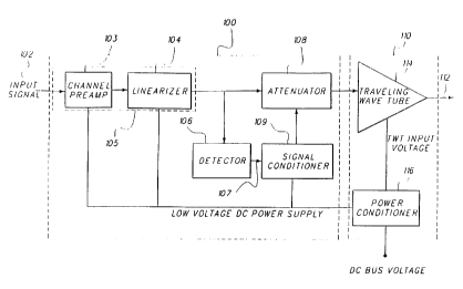
FIG. 8 is a diagram presenting a block diagram of an input drive limiter 100
implementing such a circuit. The input drive limiter i 00 comprises a detector
106 and an
attenuator 108. which are in communication with a radio frequency (RF) input
signal 102.
The input signal 102 may optionally be conditioned by a signal preconditioner
105
comprising a channel preamplifier 103 in communication with a predistortion
linearizer
'_'0 104 to increase the linearity of the output signal 112 obtained from the
amplifier 110 in
the non-saturation region. The detector I 06 dynamically produces a detector
signal 107
from the input signal 102 that is proportional to the average power of the
input signal l02
and substantially independent tcom the peak power of the input signal 102. The
detector
provides the detector signal l07 to the attenuator 108. Optionally. the
detector signal 107
is provided to the attenuator 108 via a signal conditioner 109 for purposes
described
herein.
The amplifier I 10 provides an output signal 1 1'_' at RF frequencies. and
comprises
a traveling wave tube I 1-l and a power conditioner I I O. The power
conditioner l 16
supplies a high voltage input to the traveling wave tube 1 I-t and provides
supply voltaLe
;t) to other components.
CA 02342155 2000-12-18
Generally. the ideal relationship bem~een the input signal 102 and the
detector
signal 107 is that of linear proportionalim. That is. the detector signal 107
is linearly
proportional to the input sis~nal 102. E-Iowever. it should be noted that
althous~h the
proportionalit<~ benveen the average power o1 the input signal 102 and the
detector signal
107 is ideally linear. linear proportionality between the input signal 102 and
the detector
signal 107 is not required to practice the present invention. For example. in
accordance
with the description of the attenuator 108 that follows. as a matter of design
choice. non-
linear proportionality between the input signal 102 and the detector signal
108 can be
accounted for by suitable design of the attenuator 108 to account for any such
non-
1 inearities.
FIG. 9 presents one embodiment of the input drive limner 100. As depicted in
this embodiment. the detector 106 comprises a current rectifier 202 and a low
pass filter
204. In the illustrated embodiment. the current rectifier 202 includes a diode
206 having
an anode 207 in communication with the input signal 102 provided by an input
signal
source 203 and a cathode 209 coupled to the low pass filter 204. The current
rectifier 202
converts the alternating current (AC) input signal 102 into a half wave
rectified (positive
for all values of time] signal. When this signal is low-pass filtered by the
low pass filter
?04. a detector signal 107 proportional to the average power of the input
signal 102 is
produced. It should be noted that the current rectifier'02 could be replaced
by other
'_'0 circuit elements with similar function. For example, a two-way or four-
way bridge using
four diodes can be implemented to produce a full-wave rectified signal. if
desired.
T'he low pass filter 204 comprises a resistive element 208 such as low pass
filter
resistor and a capacitive element 210 such as low pass filter capacitor.
coupled in parallel.
So coupled. the low pass titter 204 implements a circuit wherein the detector
signal 207
~5 lags the rectified signal from the diode ?06 according to a tirst order
time constant
relationship of 1 /RC.
In some circumstances. low pass tiller ?04 networks with multiple-order time
constants may be preferred. Chis selection will depend on the time duration
relationship
between the average power chances and peak power pulses in the input signal
102.
CA 02342155 2000-12-18
Thus. a matter of design choice. the low pass filter can be designed to
exhibit a steeper
tittering of input signals.
In one embodiment. the detector signal 107 is communicated directly to the
attenuator 108. which dynamically attenuates the input signal according to the
detector
signal. In another embodiment. the detector signal 107 is passed through a
signal
conditioner 212. which implements a gain relationship between the detector
signal 107
and the attenuator 108. For example. if the detector l06 fails to provide the
required
signal voltages to properly drive the attenuator circuit. the signal
conditioner can adjust
the gain of the signal or apply an impedance change to match input impedance
of the
attenuator circuit. If desired. the signal conditioner 212 can also implement
additional
low or high pass filtering, so that the dynamic characteristics of the signal
entering the
attenuator are suitable for limiting the average power of the amplifier 1 10
to a pre-
selected or dynamically determined value to prevent damage, while permitting
adequate
passage of signal peaks.
In one embodiment. the attenuator 108 comprises a shunt-Limiting device for
electrically coupling the input signal 102 to ground 226. The shunt-limiting
device can
comprise a field effect transistor (FET) 214. In the illustrated embodiment,
the FET 214
comprises a gate 216 in communication with the detector signal 107 (which, as
described
above. may be optionally processed by the signal conditioner 212). The FET 214
also
?0 comprises a source 218 in communication with the input signal 102 and a
drain in
communication with the ground 226. In one embodiment. the FET 214 is an
enhanced
FET. so that a zero voltage on the gate ? 16 is adequate to assure no shunting
of the input
signal 102 to ground. The enhancement FET is used as a voltage controlled
shunt limner
with the gate voltage provided by an average power detector circuit. The
result is a
circuit whose attenuation depends on the average power input. Alternatively,
other FET
214 types can be used. so long as they are appropriately biased (using, for
example, the
signal conditioner ? 12) to assure that the input signal 102 is shunted the
proper amount at
the proper times to effect the average power limiting function described.
ThrouLh the appropriate choice of components a limner is realized that has a
slow
s0 response time such that the peak powers of short duration pass without
attenuation while
CA 02342155 2000-12-18
the average power is limited such that the desired operating point is not
exceeded. In this
way the dynamic gain and phase response is not affected by the limner
therefore the
intermodulation distortion is not increased however the static gain and phase
response is
modified by the limner providing a protection means for the TWT 1 14. With
this limner
employed an upper level is set on the average input drive to the TWT 1 14.
FIG. 10 is a flow chart depicting representative process steps used in
perfotTning
one embodiment of the present invention. First. as shown in block 302. a value
proportional to the average power of the input signal 102 and substantially
independent
from the peak power of the input signal 102 is determined. This determination
is based
on a measurement of a time-varying input signal 102. and is hence dynamic in
nature.
Importantly, the relationship benveen the input signal and the value described
above need
not be linearly proportional, as discussed earlier in this disclosure.
Further, although the
value is substantially independent from the peak power of the input signal
102, some
residual relationship between the input signal 102 and the peak power is
permitted. For
I S example. in the embodiments described in the foregoing disclosure. the
above operations
were performed using a current rectifier 202 and a first order low pass filter
204, which
substantially attenuates input signal 102 peaks. but does not entirely
eliminate them.
Accordingly, the present invention may be practiced with some residual
manifestation of
the short duration peaks included in the detector signal 107. Hence. value
determined
?0 above need only be substantially independent from the peak power of the
input signal 102
as is required to effect the purposes of the invention as disclosed herein,
namely, limiting
the average power output. while permitting generally linear passage of the
input signal
peaks.
Next. as shown in block 304. the input signal 102 is dynamically attenuated
~5 according to the value produced above. The dynamically attenuated input
signal 102 is
then applied to an amplifier l 10.
FIG. 1 1 is a tlow chart depicting the above-described operations
ofdvnamically
determinine the value and attenuating the input sienal 102. :~s shown in
blocks 402 and
404. the input sis~nal is rectified. and low pass filtered to produce a
detector signal 107.
CA 02342155 2000-12-18
Then, the detector siLnal l07 is shunted accordine to the rectified and low
pass filtered
input signal.
Table I below presents the results of an initial analysis using computer
modeled
circuit similar to that which is disclosed in FIG. 9.
Input ~ Vd Voa Vs Vload Atten
; ~
2Asin~at)coslbt)1.? -2 0.2V 0.2V '
I ~ 0
'?Asin(on 1.5 +t 0.2V <75mV
~ i ~ 8.SdB
table 1
The detector and attenuator circuits were modeled separately. The two cases
modeled were t 1 ) two-carrier composite signal that must pass with low loss
and (2) a
single carrier signal with the same peak amplitude that must be attenuated by
at least 3dB.
.-~s illustrated in Table I. the detector signal 107 voltage shows an increase
of 0.3 volts or
about 25% when the higher average power signal is present. This voltage alone
is not
sufficient to drive the FET 214 to the desired conduction level. so a signal
conditioner
12 such as an amplifier was used to provide a three-volt level increase to
drive the FET
14 gate ? 16. When the higher average power signal is present the FET 214 is
driven
into conduction and an attenuation of 8.SdB is provided. Through adjustment of
the signal
conditioner 21'? any desired attenuation characteristics could be provided.
Conclusion
This concludes the description of the preferred embodiments of the present
''0 invention. In summary, the present invention discloses a method and
apparatus for
limiting an average power output of an amplifier without limiting the peak
power output
of the amplifier.
The method comprises the steps of dynamically detenmininL a value proportional
to an average power of an amplifier input signal and substantially independent
tom a
~5 peak power of the amplifier input siLnal. dynamically attenuating the
amplifier input
signal accordinL to the value. and applying the dynamically attenuated
amplifier input
aiLnal to an amplifier to produce the amplifier output signal.
CA 02342155 2000-12-18
he apparatus comonses a detector for ci~.wamtcailv producing a detector
sit~nai
proportional to an average power of the input signal and substantially
independent t~rom a
peak power of the input signal. and an attenuator m communication with the
detector and '
the amplifier. for dynamically attenuating the input signal according to the
detector sienal.
The present invention is particularly applicable to linearized space traveline
wave
tube systems. Vtanv systems require that the amplifiers operate at an output
back-off to
obtain linearity. typical output back-off requirements can be ~dB or more.
Unfortunately.
due to fault conditions there can be time when the amplifier is driven to its
full saturated
output power. therefore the amplifier must be capable of handling this power.
The
present invention eliminates this requirement. so that the amplifier needs
only to handle
the required operatine pow-er and not the higher fault conditions. This
results in reduced
complexity of the amplifier 1 which allows production of traveline wave tube
systems at
lower cost) and the ability to further optimize the amplifier at the operating
point (which
increases performance f.
The foregoing description of the preferred embodiment of the invention has
been
presented for the purposes of illustration and description. It is not intended
to be
exhaustive or to limit the invention to the precise form disclosed. Vtanv
modifications
and variations are possible in lieht of the above teaching. Cor example. since
the
relationship benveen the average power and the peak power is at least
partially function
~0 of the number of carriers employed in the data signal. the forecoine
invention may be
practiced by determining the number of carriers used in the signal. and using
this
determination to set the time constant or other dynamic characteristics of the
sienal
conditioner or the detector~sienal conditioner combination. i'his can be
implemented by
employine a components with variable characteristics 1 such as capacitor ? 10
or resistor
~5 =081. by switchine to one of several components with the proper
characteristics. It is also
envisioned that the signal conditioning provided by the present invention can
be
implemented by a computer or ocher processor. irnpiementing instructions for
pertormiy
.ligital liltcrtng.
ft is mtcnded that the scope co the invcnmon W limited not by this detailed
vt) ,igscrtntiun. taut rather rv the claims appended Itermo. !~lte ahoy
amcttication. ~~c;imoles
CA 02342155 2000-12-18
and data provide a compiete description ui the manufacture and use of the
composition of
she invention. since manv embodiments of the invention can tie made without
departine
from the spirit and scone of the invention. the invention resides in the
claims hereinafter
appended.