Note: Descriptions are shown in the official language in which they were submitted.
CA 02342175 2001-02-27
DESCRIPTION
TITLE OF THE INVENTION: MICROWAVE AMPLIFIER
TECHNICAL FIELD
The present invention is related to a microwave amplifier
arranged by employing a field-effect transistor.
BACKGROUND OF THE INVENTION
In general, a conventional microwave amplifier is known
from, for example, Japanese Patent Laid-open No. 285811/1986.
This first prior art will how be explained with reference to
Fig. 21.
In this drawing, reference numeral 110 shows a microwave
amplifier; reference numeral 111 indicates a field-effect
transistor (will be referred to as an "FET° ) ; reference numeral
112 represents a resistor; and reference numeral 113 shows a
connection conductor for connecting the FET 111 to the ground
plane. This connection conductor 113 functions as a tip
shortcircuit stub which contains an inductance component in a
high frequency field. Also, reference numeral 114 represents
a tip open stub, the length of which is equal to a 1 /4 wavelength
at an operating frequency of the circuit. Specifically, the 1/4
wavelenghth means a 1/4 of a wavelength. The wavelength
corresponds to the operating frequency of the circuit.
As indicated in Fig. 22; since the connection conductor
113 owns the inductance component "A", the FET 111 can be
1
CA 02342175 2001-02-27
grounded by employing only the connection conductor 113 at a
low frequency under which the inductance component "A" is
negligible. However, the inductance component "A" is not
negligible in a high frequency, and thus, a gain of the FET 111
is deteriorated. As a consequence, it is possible to avoid such
a gain deterioration of the FET 111 by employing the tip open
stub 114, so as to ground the FET 111 in the high frequency sense.
Also, at this stage, in order to suppress unwanted oscillation
of the FET 111, the resistor 112 is connected.
Next, a description will now be made of a second prior art
with reference to Fig. 23. Fig. 23 is the diagram for
representing the low noise amplifier described in "HEMT DIRECT
COOLING TYPE LOW NOISE AMPLIFIER", SHINGAKU GIRO MW 92-149,
Japanese Electronic Information Communication Institute. In
this drawing, reference numeral 120 indicates a low noise
amplifier; reference numeral 121 represents an FET; and
reference numeral 122 shows an inductor. A source electrode
of the FET 121 is grounded via the inductor 122. As a result,
the input impedance for minimizing noise of the FET 121 can be
located in the vicinity of the impedance for minimizing the
reflection, and also both the noise figure and the reflection
coefficient o~n the input side can be improved at the same time.
On the other hand, any of the above-described prior art
owns the below-mentioned problems. First, the microwave
amplifier 110 corresponding to the first prior art owns such
2
CA 02342175 2001-02-27
a problem that unnecessary electric power is consumed by the
resistor 112 connected to the source electrode of the FET 111,
and thus, the output power characteristic would be deteriorated.
Also, as shown in Fig. 24, the low noise amplifier 120
corresponding to the second prior art owns such a problem that
since the inductor 122 connected to the source electrode of the
FET 121 owns the stray capacitance "B", this inductor is
resonated at a predetermined frequency, and thus, operation
would become unstable.
The present invention has an object to solve these
problems.
DISCLOSURE OF THE INVENTION
A microwave amplifier, according to the present invention,
is featured by such a microwave amplifier arranged by employing
a field-effect transistor, wherein: both an inductor and a
resistor are loaded in a parallel manner between a source
electrode of the field-effect transistor and the ground.
Also, a microwave amplifier, according to the present
invention, is featured by such a microwave amplifier arranged
by employing a field-effect transistor, wherein: a first
inductor and a stabilizing circuit are loaded in a parallel
manner between a source electrode of said ffield-effect
transistor and the ground; and the stabilizing circuit is
equipped with a second inductor and a resistor series-connected
to the second inductor, the second inductor is resonated at a
3
CA 02342175 2001-02-27
frequency different from another frequency at which the first
inductor is resonated by a stray capacitance component.
Further, a~ microwave amplifier, according to the present
invention, is featured by such a microwave amplifier arranged
by employing a field-effect transistor, wherein: a first
inductor and a stabilizing circuit are loaded in a parallel
manner between a source electrode of the field-effect
transistor and the ground; the stabilizing circuit is equipped
with a resonant unit in which a second inductor is
parallel-connected to a capacitor, and a resistor series-
connected to the resonant unit; and the resonant unit is
resonated at a frequency different from another frequency at
which the first inductor is resonated by a stray capacitance
component.
Also, a microwave amplifier, according to the present
invention, is featured by such a microwave amplifier arranged
by employing a field-effect transistor, wherein: a first
inductor and a stabilizing circuit are loaded in a parallel
manner between a source electrode of the field-effect
transistor and the ground; the stabilizing circuit is equipped
with a resonant unit in which a second inductor is series-
connected to(a capacitor, and a resistor series-connected to
the resonant unit; and the resonant unit is resonated at a
frequency different from another frequency at which the first
inductor is resonated by a stray capacitance component.
4
CA 02342175 2001-02-27
Further, a microwave amplifier, according to the present
invention, is featured by such a microwave amplifier arranged
by employing a field-effect transistor, wherein: an inductor
and a stabilizing circuit are loaded in a parallel manner between
a source electrode of the field-effect transistor and the
ground; the stabilizing circuit is equipped with a short stub
and a resistor series-connected to the short stub; and a length
of the short stub is equal to a 1/2 wavelength at a frequency
where the inductor is resonated by a stray capacitance
component.
Further, a microwave amplifier, according to the present
invention,, is featured by such a microwave amplifier arranged
by employing a field-effect transistor, wherein: an inductor
and a stabilizing circuit are loaded in a parallel manner between
a source electrode of the field-effect transistor and the
ground; and the stabilizing circuit is equipped with a short
stub and a resistor series-connected to the short stub; and a
length of the short stub is equal to a 1/4 wavelength at a
frequency different from such a frequency that the inductor is
resonated by a stray capacitance_component.
Also, a microwave amplifier, according to the present
invention, i~ featured by such a microwave amplifier arranged
by employing a field-effect transistor, comprising: an inductor
loaded between a source electrode of the field-effect
transistor and the ground; a resistor, one end of which is
CA 02342175 2001-02-27
connected to the electrode; and an open stub connected to the
other end of the resistor, the length of which is equal to a
1 /2 wavelength at a frequency where the inductor is resonated
by a stray capacitance component.
Further, a microwave amplifier, according to the present
invention, is featured by such a microwave amplifier arranged
by employing a field-effect transistor, comprising: an inductor
loaded between a source electrode of the field-effect
transistor and the ground; a resistor, one end of which is
connected to the electrode; and an open stub connected to the
other end of the resistor, the length of which is equal to a
1/4 wavelength at a frequency different from such a frequency
that the inductor is resonated by a stray capacitance component.
Also, a microwave amplifier, according to the present
invention, is featured by such a microwave amplifier arranged
by employing a field-effect transistor, comprising: an inductor
loaded between a source electrode of the field-effect
transistor and the ground; a resistor connected between a drain
electrode of the field-effect transistor and an output
terminal; and a bias circuit connected between the drain
electrode of the field-effect transistor and the ground.
In this Ease, the bias circuit is preferably equipped with
an RF choke inductor, and a bypass capacitor series-connected
to the RF choke inductor.
Further, a microwave amplifier, according to the present
6
CA 02342175 2001-02-27
invention, is featured by such a microwave amplifier arranged
by employing a field-effect transistor, comprising: an inductor
loaded between a source electrode of the field-effect
transistor and the ground; a resistor connected between a gate
electrode of the field-effect transistor and an input terminal;
and a bias circuit connected between the input terminal and the
ground.
In this case, the bias circuit is equipped with an RF choke
inductor, and a bypass capacitor series-connected to the RF
choke inductor.
' BRIEF DESCRIPTION OF THE DRAWINGS
Fig. 1 is a circuit diagram for representing a microwave
amplifier according to an embodiment mode 1.
Fig. 2 is an equivalent circuit diagram of the microwave
amplifier according to the embodiment mode 1.
Fig. 3 is a circuit diagram for showing a microwave
amplifier according to an embodiment mode 2.
Fig. 4 is an equivalent circuit diagram of the microwave
amplifier according to the embodiment mode 2.
Fig. 5 is a circuit diagram for indicating a microwave
amplifier according to an embodiment mode 3.
Fig. 6 .ids an equivalent circuit diagram of the microwave
amplifier according to the embodiment mode 3.
_ Fig. 7 is a circuit diagram for showing a microwave
amplifier according to an embodiment mode 4.
7
CA 02342175 2001-02-27
Fig. 8 is an equivalent circuit diagram of the microwave
amplifier according to the embodiment mode 4.
Fig. 9 is a circuit diagram for indicating a microwave
amplifier according to an embodiment mode 5.
Fig. 10 is an equivalent circuit diagram of the microwave
amplifier according to the embodiment mode 5.
Fig. 11 is a circuit diagram for showing a microwave
amplifier according to an embodiment mode 6.
Fig. 12 is an equivalent circuit diagram of the microwave
amplifier according to the embodiment mode 6.
Fig. 13 is a circuit diagram for indicating a microwave
amplifier according to an embodiment mode 7.
Fig. 14 is an equivalent circuit diagram of the microwave
amplifier according to the embodiment mode 7.
Fig. 15 is a circuit diagram for showing a microwave
amplifier according to an embodiment mode 8.
Fig. 16 is an equivalent circuit diagram'of the microwave
amplifier according to the embodiment mode 8.
Fig. 17 is a circuit diagram for indicating a microwave
amplifier according to an embodiment mode 9.
Fig. 18 is an equivalent circuit diagram of the microwave
amplifier according to the embodiment mode 9.
Fig. 19 is a circuit diagram for showing a microwave
amplifier according to an embodiment mode 10.
Fig. 20 is an equivalent circuit diagram of the microwave
8
CA 02342175 2001-02-27
amplifier according to the embodiment mode 10.
Fig. 21 is the circuit diagram for indicating the microwave
amplifier according to the first prior art.
Fig. 22 is the equivalent circuit diagram of the microwave
amplifier according to the first prior art.
Fig. 23 is the circuit diagram for indicating the low noise
amplifier according to the second prior art.
Fig. 24 is the equivalent circuit diagram of the low noise
amplifier according to the second prior art.
BEST MODE FOR CARRYING OUT THE INVENTION
Referring now to the accompanying drawings, an embodiment
mode of the present invention will be described.
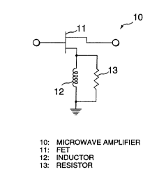
EMBODIMENT MODE 1
Fig. 1 is a circuit diagram for showing a microwave
amplifier according to an embodiment mode 1.
In this drawing, reference numeral 10 indicates a source
grounded type microwave amplifier; reference numeral 11 shows
an FET; reference numeral 12 represents an inductor loaded
between a source electrode of the FET 11 and the ground; and
reference numeral 13 indicates a resistor loaded between the
source electrode of the FET 11 and the ground and also connected
in parallel to the inductor 12.
Next, operations will now be explained. A signal applied
to the source electrode is amplified by the FET 11, and then
the amplified signal is derived from a drain electrode of the
9
CA 02342175 2001-02-27
FET 11. Since the inductor 12 is loaded between the source
electrode of the FET 11 and the ground, an input impedance
capable of minimizing noise of the FET 11 can. be located in the
vicinity of an impedance capable of minimizing a reflection of
the FET 11, and both a noise characteristic and a reflection
characteristic can be improved at the same time.
Also, since the inductor 12 is formed on either a
semiconductor chip or a semiconductor substrate, as shown in
Fig. 2, the inductor 12 contains a stray capacitance component
B. As a result, the inductor 12 is brought into such a conduction
that this inductor 12 is parallel-connected to a capacitor, so
that a parallel resonant circuit 14 is constituted. Then, the
inductor 12 is resonated at the frequency of "f0" by this stray
capacitance component B, and thus, the parallel resonant
circuit 14 is brought into an open state. However, since the
inductor 12 is loaded in parallel to the resistor 13, the source
electrode of the FET 11 can be grounded via'the resistor 13,
and unwanted oscillation of the FET 11 in the frequency range
of the frequency "f0" may be suppressed. As a result, the
operation of the microwave amplifier 10 at the resonant
frequency "f0" may be stabilized.
It shou~d be understood that the FET 11, the inductor 12,
and the resistor 13 may be formed on a single semiconductor
substrate, or may be separately formed on independent
semiconductor chips. Alternatively, a partially selected
CA 02342175 2001-02-27
element of these FET 11, inductor 12, and resistor 13 may be
formed on a semiconductor chip, and other elements may be formed
on a semiconductor substrate.
EMBODIMENT MODE 2
Next, a microwave amplifier according to an embodiment
mode 2 will now be explained with reference to Fig. 3. In this
drawing, reference numeral 20 shows a source grounded type
microwave amplifier; reference numeral 21 indicates an FET;
reference numeral 22 represents an inductor (first inductor)
loaded~between a source electrode of the FET 21 and the ground;
and reference numeral 23 indicates a stabilizing circuit loaded
between the source electrode of the FET 21 and the ground and
also loaded in parallel to the inductor 22 : In this case, -the
stabilizing circuit 23 is equipped with a resistor 24 whose one
end is connected to the source electrode of the FET 21, and
another inductor (second inductor) 25 connected in series to
the other end of the resistor 24.
Next, operations will now be explained. A signal applied
to the source electrode .is amplified by the FET 21, and then
the amplified signal is derived from a drain electrode of the
FET 21. Since the inductor 22 is loaded between the source
electrode of~the FET 21 and the ground, an input impedance
capable of minimizing noise of the FET 21 can be located in the
vicinity of an impedance capable of minimizing a reflection of
the FET 21, and both a noise characteristic and a reflection
11
CA 02342175 2001-02-27
characteristic can be improved at the same time.
Also, since the inductors 22 and 25 are formed on either
a semiconductor chip or a semiconductor substrate, as shown in
Fig. 4, the inductor 22 contains a stray capacitance component
B, and the inductor 25 owns a stray capacitance component C
(stray capacitances of B and C are different from each other).
As a consequence, the inductors 22 and 25 are brought into such
a condition that these inductors are connected in parallel to
the capacitors, so that a parallel resonant circuit 26 resonated
at a frequency "f0" is arranged by the inductor 22 and the stray
capacitance component B. Also, another parallel resonant
circuit 27 resonated at a frequency "fc" (namely, operating
frequency of circuit) different from the frequency "f0" is
arranged by the inductor 25 and the stray capacitance component
C.
As a consequence, in such a case that the microwave
amplifier 20 is used at the frequency "fc", the inductor 22 is
operated under normal condition without being resonated. On
the other hand, since the inductor 25 is resonated at the
frequency "fc", the parallel resonant circuit 27 constructed
of the inductor 25 and the stray capacitance component C is
brought intotan open state.
Therefore, the following equivalent circuit may be
constructed. That is, only the inductor 22 is connected to the
source electrode of the FET 21.
12
CA 02342175 2001-02-27
. As a result, at the frequency "fc", the. noise matching
impedance can be located in the vicinity of the reflection
matching impedance by way of the inductor 22, and also both the
noise characteristic and the reflection characteristic can be.
improved at the same time. Also, in this case, since no current
will flow through the resistor 24, the power consumption can
be suppressed and the output power characteristic can be
improved.
Next, in the case that the microwave amplifier 20 is used
at the frequency "f0", the inductor 22 is resonated by the stray
capacitance component B, and the parallel resonant circuit 26
constructed of the inductor 22 and the stray capacitance
component B is brought into an open state. On the other hand,
the inductor 25 is operated normally at the frequency "f0"
without being resonated. As a consequence, the following
equivalent circuit may be constructed. That is, only the
resistor 24 and the inductor 25 are connected to the source
electrode of the FET 21.
As a result, at the frequency "f 0 " , the source electrode
of the FET 21 can be grounded via the resistor 24, and unwanted
oscillation of the FET 21 may be suppressed. As a result, the
operation o~ the microwave amplifier 20 at the resonant
frequency "f0" may be stabilized.
It should be understood that the FET 21, the inductors 22
and 25, and the resistor 24 may be formed on a single
13
CA 02342175 2001-02-27
semiconductor substrate, or may be separately formed on
independent semiconductor chips. Alternatively, a partially
selected element of these FET 21, inductors 22 and 25, and
resistor 24 may be formed on a semiconductor chip, and other
elements may be formed on a semiconductor substrate.
EMBODIMENT MODE 3
Next, a microwave amplifier according to an embodiment
mode 3 will now be explained with reference to Fig. 5. In this
drawing, reference numeral 30 shows a source grounded type
microwave amplifier; reference numeral 31 indicates an FET;
reference numeral 32 represents an inductor (first inductor)
loaded between a source electrode of the FET 31 and the ground;
and reference numeral 33 indicates a stabilizing circuit loaded
between the source electrode of the FET 31 and the ground and
also loaded in parallel to the inductor 32. In this case, the
stabilizing circuit 33 is equipped with a resonant unit 36, and
a resistor 37 . The resonant unit 36 is equipped with an inductor
( second inductor ) 34 and a capacitor 35 connected in parallel
to each other. This resistor 37 is connected in series with
the resonant circuit 36.
Next, operations will now be explained. A signal applied
to the sources electrode is amplified by the FET 31, and then
the amplified signal is derived from a drain electrode of the
FET 31. Since the inductor 32 is loaded between the source
electrode of the FET 31 and the ground, an input impedance
14
CA 02342175 2001-02-27
capable of minimizing noise of the FET 31 can be located in the
vicinity of an impedance capable of minimizing a reflection of
the FET 31, and both a noise characteristic and a reflection
characteristic can be improved at the same time.
Also, since the inductors 32 and 34 are formed on either
a semiconductor chip or a semiconductor substrate, as shown in
Fig. 6, the inductors 32 and 34 own stray capacitance components
B, respectively. As a consequence, the inductors 33 and 34 are
brought into such a condition that these inductors are connected
in parallel to the capacitors, so that a parallel resonant
circuit 38 resonated at a frequency "f0" is arranged by the
inductor 32 and the stray capacitance component B. Also,
another parallel resonant circuit 39 resonated at a frequency
"fc" (namely, operating frequency of circuit) different from
the frequency "f0" is arranged by the inductor 34, the stray
capacitance component B and capacitor 35.
As a consequence, in such a case that the microwave
amplifier 30 is used at the frequency "fc", the inductor 32 is
operated under normal condition without being resonated. On
the other hand, the parallel resonant circuit 39 constructed
of the inductor 34, the stray capacitance component B and
capacitor 35 ~.s resonated at the frequency "fc" , and is brought
into an open\state. Therefore, the following equivalent
circuit may be constructed. That is, only the inductor 32 is
connected to the source electrode of the FET 31.
CA 02342175 2001-02-27
As a result, at the frequency "fc", the noise matching
impedance can be located in the vicinity of the reflection
matching ~.mpedance by way of the inductor 32, and also both the
noise characteristic and the reflection characteristic can be
improved at the same time. Also, in this case, since no current
will flow through the resistor 37, the power consumption can
be suppressed and the output power characteristic can be
improved.
Next, in the case that the microwave amplifier 30 is used
at the frequency "f0", the inductor 32 is resonated by the stray
capacitance component B, and the parallel resonant circuit 38
constructed of the inductor 32 and the stray capacitance
component B is brought into an open state. On the other hand,
the inductor 34 is operated under normal condition without being
resonated at the frequency "f0". As a consequence, the
following equivalent circuit may be constructed. That is, only
the resistor 37 and the resonant unit 36 are connected to the
source electrode of the FET 31.
As a result, at the frequency "f0", the source electrode
of the FET 31 can be grounded via the res istor 3 7 , and unwanted
oscillation of the FET 31 may be suppressed. As a result, the
operation ofd the microwave amplifier 30 at the resonant
frequency "f0" may be stabilized.
_ It should be noted that i;n this embodiment mode, since the
capacitor 35 is added in parallel to the inductor 34, the
16
CA 02342175 2001-02-27
resonant frequency of the parallel resonant circuit 39 is
adjusted to become "fc" . As a result, the inductor 34 may be
manufactured in such a manner that this inductor 34 owns the
same stray capacitance component B as that of the inductor 32,
and the manufacturing,step can become simple.
It should be also understood that the FET 31, the inductors
32 and 34, capacitor 35, and the resistor 37 may be formed on
a single semiconductor substrate, or may be separately formed
on independent semiconductor chips. Alternatively, a
partially selected element of these FET 31, inductors 32 and
34, capacitor 35, and resistor 37 may be formed on a
semiconductor chip, and other elements may be formed on a
semiconductor substrate.
EMBODIMENT MODE 4
Next, a microwave amplifier according to an embodiment
mode 4 will now be explained with reference to Fig. 7. In this
drawing, reference numeral 40 shows a source grounded type
microwave amplifier; reference numeral 41 indicates an FET;
reference numeral 42 represents an inductor (first inductor)
loaded between a source electrode of the FET 41 and the ground;
and reference numeral 43 indicates a stabilizing circuit loaded
between the source electrode of the FET 41 and the ground and
also loaded in parallel to the inductor 42. In this case, the
stabilizing circuit 43 is equipped with a resonant unit 46, and
a resistor 47. The resonant unit 46 is equipped with an inductor
17
CA 02342175 2001-02-27
(second inductor) 44 and a capacitor 45 connected in series to
each other. This resistor 47 is connected in series with the
resonant circuit 46.
Next, operations will now be explained. A signal applied
to the source electrode is amplified by the FET 41, and then
the amplified signal is derived from a drain electrode of the
FET 41. Since the inductor 42 is loaded between the source
electrode of the FET 41 and the ground, an input impedance
capable of minimizing noise of the FET 41 can be located in the
vicinity of an impedance capable of minimizing a reflection of
the FET 41, and both a noise characteristic and a reflection
characteristic can be improved at the same time.
Also, since the inductors 42 and 44 are formed on either
a semiconductor chip or a semiconductor substrate, as shown in
Fig . 8 , the inductor 4 2 contains a stray capacitance component
B, and the inductor 44 owns a stray capacitance component C.
As a consequence, the inductors 42 and 44 are brought into such
a condition that these inductors are connected in parallel to
the capacitors, so that a parallel resonant circuit 48 resonated
at a frequency "f0" is arranged by the inductor 42 and the stray
capacitance component H. Also, a series resonant circuit 49
resonated at the frequency "f0" is arranged by the inductor 44,
the capacitor\45, and the stray capacitance component C.
As a consequence, in such a case that the microwave
amplifier 40 is used at frequencies other than the frequency
18
CA 02342175 2001-02-27
" f 0 " , the inductors 4 2 and 4 4 are operated under normal condition
without being resonated. As a result, at the frequencies other
than the frequency "f0", the noise matching impedance can be
located in the vicinity of the reflection matching impedance
by way of the inductor 42, and also both the noise characteristic
and the reflection characteristic can be improved at the same
time.
Next, in the case that the microwave amplifier 40 is used
at the frequency "f0", the inductor 42 is resonated by the stray
capacitance component B, and the parallel resonant circuit 48
constructed of the inductor 42 and the stray capacitance
component B is brought into an open state . On the other hand,
the series resonant circuit 49 constructed of the inductor 44,
the stray capacitance component C, and the capacitor 45 is
resonated at the frequency "f0" to be shortcircuited. As a
consequence, the following equivalent circuit may be
constructed. That is, only the resistor 47 is connected to the
source electrode of the FET 41.
As a result, at the frequency "f0", the source electrode
of the FET 4l can be grounded via the resistor 47, and unwanted
oscillation of the FET 41 may be suppressed. As a result, the
operation of the microwave amplifier 40 at the resonant
frequency "f0" may be stabilized.
It should be understood that the FET 41, the inductors 42
and 44, the capacitor 45, and the resistor 47 may be formed on
19
CA 02342175 2001-02-27
a single semiconductor substrate, or may be separately formed .
on independent semiconductor chips. Alternatively, a
partially selected element of these FET 41, inductors 42 and
44, the capacitor 45, and resistor 47 may be formed on a
semiconductor chip, and other elements may be formed on a
semiconductor substrate.
EMBODIMENT MODE 5
Next, a microwave amplifier according to an embodiment
mode 5 will now be explained with reference to Fig. 9. In this
drawing, reference numeral 50 shows a source grounded type
microwave amplifier; reference numeral 51 indicates an FET;
reference numeral 52 represents an inductor loaded between a
source electrode of the FET 51 and the ground; and reference
numeral 53 indicates a stabilizing circuit loaded between the
source electrode of the FET 51 and the ground and also loaded
in parallel to the inductor 52. In this case, the stabilizing
circuit 53 is equipped with a resistor 54 whose one end is
connected to the source electrode of the FET 51, and a short
stub 55 connected in series to the other end of the resistor
54.
Next, operations will now be explained. A signal applied
to the source electrode is amplified by the FET 51, and then
the amplified 'signal is derived from a drain electrode of the
FET 51. Since the inductor 52 is loaded between the source
electrode of the FET 51 and the ground, an input impedance
CA 02342175 2001-02-27
capable of minimizing noise of the FET 51 can be located in the
vicinity of an impedance capable of minimizing a reflection of
the FET 51, and both a noise characteristic and a reflection
characteristic can be improved at the same time.
Also, since the inductor 52 is formed on either a
semiconductor chip or a semiconductor substrate, as shown in
Fig. 10, the inductor 52 contains a stray capacitance component
B. As a consequence, the inductor 52 is brought into such a
condition that this inductor is connected in parallel to the
capacitor, so that a parallel resonant circuit 56 resonated at
a frequency "f0" is arranged by the inductor 52 and the stray
capacitance component B. On the other hand, the short stub 55
is adjusted in such a manner that the length of this short stub
55 is equal to a 1/2 wavelength at the frequency "f0".
As a consequence, in such a case that the microwave
amplifier 50 is used at the frequency "fc" (operating frequency
of circuit ) , the inductor 52 is operated under normal condition
without being resonated.
Then, at the frequency "fc", the noise matching impedance
can be located in the vicinity of the reflection matching
impedance by way of the inductor 52, and also both the noise
characterist~ic~ and the reflection characteristic can be
improved at the same time. Also, in this case, since the short
stub 55 becomes a high impedance, the power consumption caused
by the resistor 54 can be suppressed and the output power
21
CA 02342175 2001-02-27
characteristic can be improved.
Next, in the case that the microwave amplifier 50 is used
at the frequency "f0", the inductor 52 is resonated by the stray
capacitance component B, and the parallel resonant circuit 56
constructed of the inductor 52 and the stray capacitance
component B is brought into an open state. On the other hand,
the short stub 55 is shortcircuited at the frequency "f0" . As
a consequence, the following equivalent circuit may be
constructed . That is , only the res istor 54 is connected to the
source electrode of the FET 51.
As a result, at the frequency "f0", the source electrode
of the FET 51 can be grounded via the resistor 54, and unwanted
oscillation of the FET 51 may be suppressed. As a result, the
operation of the microwave amplifier 50 at the resonant
frequency "f0" may be stabilized.
It should be understood that the FET 51, the inductor 52,
the short stub 55, and the resistor 54 may be formed on a single
semiconductor substrate, or may be separately formed on
independent semiconductor chips. Alternatively, a partially
selected element of these FET 51, inductor 52, short stub 55,
and resistor 54 may be formed on a semiconductor chip, and other
elements maybe formed on a semiconductor substrate.
EMBODIMENT MODE 6
Next, a microwave amplifier according to an embodiment
mode 6 will now be explained with reference to Fig. 11. In this
22
CA 02342175 2001-02-27
drawing, reference numeral 60 shows a source grounded type
microwave amplifier; reference numeral 61 indicates an FET;
reference numeral 62 represents an inductor loaded between a
source electrode of the FET 61 and the ground; and reference
numeral 63 indicates a stabilizing circuit loaded between the
source electrode of the FET 61 and the ground and also loaded
in parallel to the inductor 62. In this case, the stabilizing
circuit 63 is equipped with a resistor 64 whose one end is
connected to the source electrode of the FET 61, and a short
stub 65 connected in series to the other end of the resistor
64.
Next, operations will now be explained. A signal applied
to the source electrode is amplified by the FET 61, and then
the amplified signal is derived from a drain electrode of the
FET 61. Since the inductor 62 is loaded between the source
electrode of the FET 61 and the ground, an input impedance
capable of minimizing noise of the FET 61 can be located in the
vicinity of an impedance capable of minimizing a reflection of
the FET 61, and both a noise characteristic and a reflection
characteristic can be improved at the same time.
Also, since the inductor 62 is formed on either a
semiconductor chip or a semiconductor substrate, as shown in
Fig. 12, the inductor 62 contains a stray capacitance component
H-. As a consequence, the inductor 62 is brought into such a
condition that this inductor is connected in parallel to the
23
CA 02342175 2001-02-27
capacitors so that a parallel resonant circuit 66 resonated at
a frequency "f0" is arranged by the inductor 62 and the stray
capacitance component B. On the other hand, the short stub 65
is adjusted in such a manner that the length of the short stub
65 is equal to a 1/4 wavelength at the frequency "fc" (operating
frequency of circuit ) . As a result, the short stub 65 is brought
into an open state of the frequency "fc".
As a consequence, in such a case that the microwave
amplifier 60 is used at the frequency "fc", the inductor 62 is
operated under normal condition without being resonated.
Then, at the frequency "fc" , the noise matching impedance
can be located in the vicinity of the reflection matching
impedance by way of the inductor 62, and also both the noise
characteristic and the reflection characteristic can be
improved at the same time. Also, in this case, since the short
stub 65 is opened, no current will flow through the resistor
64. Accordingly, the power consumption can be suppressed and
the output power characteristic can be improved.
Next, in the case that the microwave amplifier 60 is used
at the frequency "f0", the inductor 62 is resonated by the stray
capacitance component B, and the parallel resonant circuit 66
constructed Pf the inductor 62 and the stray capacitance
component B is\brought into an open state. As a consequence,
the following equivalent circuit may be constructed. That is,
only the resistor 64 is connected to the source electrode of
24
CA 02342175 2001-02-27
the FET 61.
As a'result, at the frequency "f0", the source electrode
of the FET 61 can be grounded via the resistor 64, and unwanted
oscillation of the FET 61 may be suppressed. As a result, the
operation of the microwave amplifier 60 at the resonant
frequency "f0" may be stabilized.
It should be understood that the FET 61, the inductor 62,
the resistor 64, and the short stub 65 may be formed on a single
semiconductor substrate, or may be separately formed on
independent semiconductor chips. Alternatively, a partially
selected element of these FET 61, inductor 62, resistor 64, and
short stub 65 may be formed on a semiconductor chip, and other
elements may be formed on a semiconductor substrate.
EMBODIMENT MODE 7
Next, a microwave amplifier according to an embodiment '
mode 7 will now be explained with reference to Fig. 13. In this
drawing, reference numeral 70 shows a source grounded type
microwave amplifier; reference numeral 71 indicates an FET;
reference numeral 72 represents an inductor loaded between a
source electrode of the FET 71 and the ground; and reference
numeral 73 shows a resistor whose one end is connected to the
source electrode of the FET 71, and reference numeral 74 is an
open stub connected in series to the other end of the resistor
73.
Next, operations will now be explained. A signal applied
CA 02342175 2001-02-27
to the source electrode is amplified by the FET 71, and then
the amplified signal is derived from a drain electrode of the
FET 71. Since the inductor 72 is loaded between the source
electrode of the FET 71 and the ground, an input impedance
capable of minimizing noise of the FET 71 can be located in the
vicinity of an impedance capable of minimizing a reflection of
the FET 71, and both a noise characteristic and a reflection
characteristic can be improved at the same time.
Also, since the inductor 72 is formed on either a
semiconductor chip or a semiconductor substrate, as shown in
Fig. 14, the inductor 72 contains a stray capacitance component
B. As a consequence, the inductor 72 is brought.into such a
condition that this inductor is connected in parallel to the
capacitor, so that a parallel resonant circuit 75 resonated at
a frequency "f0" is arranged by the inductor 72 and the stray
capacitance component B. On the other hand, the open stub 74
is adjusted in such a manner that the length' of the open stub
74 is equal to a 1/2 wavelength at the frequency "fc" (operating
frequency of circuit ) . As a result, the open stub 74 is brought
into an open state at the frequency "fc".
As a consequence, in such a case that the microwave
amplifier 70 his used at the frequency "fc" , the inductor 72 is
operated under normal condition without being resonated.
Then, at the frequency "fc", the noise matching impedance
can be located in the vicinity of the reflection matching
26
CA 02342175 2001-02-27
impedance by way of the inductor 72, and also both the noise
characteristic and the reflection characteristic can be
improved at the same time. Also, in this case, since the open
stub 74 is opened, no current will flow through the resistor
73. As a result, the power consumption can be suppressed and
the output power characteristic can be improved.
Next, in the case that the microwave amplifier 70 is used
at the frequency "f0" , the inductor 72 is resonated by the stray
capacitance component B, and the parallel resonant circuit 75
constructed of the inductor 72 and the stray capacitance
component B is brought into an open state. As a consequence,
the following equivalent circuit may be constructed. That is,
only the resistor 74 is connected to the source electrode of
the FET 71.
As a result, at the frequency "f0", the source electrode
of the FET 71 can be grounded via the resistor 74. As a result,
the operation of the microwave amplifier 70 at the resonant
frequency "f0" may be stabilized.
It should be understood that the FET 71, the inductor 72,
the resistor 73, and the open stub 74 may be formed on a single
semiconductor substrate, or may be separately formed on
independent semiconductor chips. Alternatively, a partially
selected element of these FET 71, inductor 72, resistor 73, and
open stub 74 may be formed on' a semiconductor chip, and other
elements may be formed on a semiconductor substrate.
27
CA 02342175 2001-02-27
EMBODIMENT MODE 8
Next, a microwave amplifier according to an embodiment
mode 8 will now be explained with reference to Fig. 15. In this
drawing, reference numeral 80 shows a source grounded type
microwave amplifier; reference numeral 81 indicates an FET;
reference numeral 82 represents an inductor loaded between a
source electrode of the FET 81 and the ground; and reference
numeral 83 indicates a resistor whose one end is connected to
the source electrode of the FET 81, and reference numeral 84
is an open stub connected in series to the other end of the
resistor 83.
Next, operations will now be explained. A signal applied
to the source electrode is amplified by the FET 8l, and then
the amplified signal is derived from a drain electrode of the
FET 81. Since the inductor 82 is loaded between the source
electrode of the FET 81 and the ground, an input impedance
capable of minimizing noise of the FET 81 can be located in the
vicinity of an impedance capable of minimizing a reflection of
the FET 81, and both a noise characteristic and a reflection
characteristic can be improved at the same time.
Also, since the inductor 82 is formed on either a
semiconductor chip or a semiconductor substrate, as shown in
Fig. 16, the inductor 82 contains a stray capacitance component
B. As a consequence, the inductor 82 is brought into such a
condition that this inductor is connected in parallel to the
28
CA 02342175 2001-02-27
capacitor, so that a parallel resonant circuit 85 resonated at
a frequency "f0" is arranged by the inductor 82 and the stray
capacitance component B. On the other hand, the open stub 84
is adjusted in such a manner that the length of this open stub
84 is equal to a 1/4 wavelength at the frequency "f0" . Therefore,
the open stub 84 is shortcircuited at the frequency "f0".
As a consequence, in such a case that the microwave
amplifier 80 is used at a frequency "fc" (operating frequency
of circuit ) , the inductor 82 is operated under normal condition
without being resonated.
Then, at the frequency "fc", the noise matching impedance
can be located in the vicinity of the reflection matching
impedance by way of the inductor 82, and also both the noise
characteristic and the reflection characteristic can be
improved at the same time. Also, in this case, since the open
stub 84 becomes a high impedance, the power consumption caused
by the resistor 83 can be suppressed and the output power
characteristic can be improved.
Next, in the case that the microwave amplifier 80 is used
at the frequency "f0", the inductor 82 is resonated by the stray
capacitance component B, and the parallel resonant circuit 85
constructed tof the inductor 82 and the stray capacitance
component B is' brought into an open state. On the other hand,
the open stub 84 is shortcircuited at the frequency "f0" . As
a consequence, the following equivalent circuit may be
29
CA 02342175 2001-02-27
constructed. That is, only the resistor 83 is connected to the
source electrode of the FET 81.
As a result, at the frequency "f0", the source electrode
of the FET 81 can be grounded via the res istor 83 , and unwanted
oscillation of the FET 81 may be suppressed. As a result, the
operation of the microwave amplifier 80 at the resonant
frequency "f0" may be stabilized.
It should be understood that the FET 81, the inductor 82,
the resistor 83, and the open stub 84 may be formed on a single
semiconductor substrate, or may be separately formed on
independent semiconductor chips. Alternatively, a partially
selected element of these FET 81, inductor 82, the resistor 83,
and open stub 84 may be formed on a semiconductor chip, and other
elements may be formed on a semiconductor substrate.
EMBODIMENT MODE 9
Next, a microwave amplifier according to an embodiment
mode 9 will now be explained with reference to Fig. 17. In this
drawing, reference numeral 90 shows a source grounded type
microwave amplifier; reference numeral 91 indicates an FET;
reference numeral 92 represents an inductor loaded between a
source electrode of the FET 91 and the ground; reference numeral
93 indicates ~; resistor connected between a drain electrode of
the FET 91 and an output terminal; and reference numeral 94
represents a bias circuit connected between the drain electrode
of the FET 91 and the ground. In this case, the bias circuit
CA 02342175 2001-02-27
94 is equipped with an RF choke inductor 95, a bypass capacitor
96, and a bias terminal 97. One end of the RF choke inductor
95 is connected to the drain electrode of the FET 91. One end
of the bypass capacitor 96 is connected to the RF choke inductor
95, and the other end thereof is grounded. The bias terminal
97 is connected between the RF choke inductor 95 and the bypass
capacitor 96.
Next, operations will now be explained. A signal applied
to the source electrode is amplified by the FET 91, and then
the amplified signal is derived from a drain electrode of the
FET 91. Since the inductor 92 is loaded between the source
electrode of the FET 91 and the ground, an input impedance
capable of minimizing noise of the FET 91 can be located in the
vicinity of an impedance capable of minimizing a reflection of
the FET 91, and both a noise characteristic and a reflection
characteristic can be improved at the same time.
Also, since the inductor 92 is formed on either a.
semiconductor chip or a semiconductor substrate, as shown in
Fig. 18, the inductor 92 contain a stray capacitance component
B. As a consequence, the inductor 92 is brought into such a
condition that this inductor is connected in parallel to the
capacitors, s<o that a parallel resonant circuit 98 resonated
at a frequency '~ f 0 " is arranged by the inductor 92 and the stray
capacitance component B.
As a consequence, in such a case that the microwave
31
CA 02342175 2001-02-27
amplifier 90 is used at a frequency "f0", the inductor.92 is
resonated at the frequency "f0" by the stray capacitance
component B, the parallel resonant circuit 98 constructed of
the inductor 92 and the stray capacitance component B is brought
into an open state. However, since the resistor 93 is
series-connected to the drain electrode of the FET 91 and the
bias voltage is applied to the drain electrode of the FET 91
from the bias circuit 94, even when the parallel resonant circuit
98 is opened, the operation of the microwave amplifier 90 may
be stabilized. Also, since no resistor is connected to the
source electrode of the FET 91, an occurrence of noise caused
by the resistor connected to the source electrode can be
suppressed.
Also, since the resistor 93 is series-connected to the
drain electrode of the FET 91, the operation of the microwave
amplifier 90 may be stabilized over the entire frequency range
without any frequency selection. As a consequence, the
microwave amplifier 90 may become such a low noise amplifier
operable understable condition, while the noise characteristic
is substantially not deteriorated.
EMBODIMENT MODE 10
Next, a microwave amplifier according to an embodiment
mode 10 will now be explained with reference to Fig. 19. In
this drawing, reference numeral 100 shows a source grounded type
microwave amplifier; reference numeral 101 indicates an FET;
32
CA 02342175 2001-02-27
reference numeral 102 represents an inductor loaded between a
source electrode of the FET 101 and the ground; reference numeral
103 indicates a resistor connected to a gate electrode of the
FET 101 and an input terminal; and reference numeral 104
represents a bias circuit connected between the input terminal
and the ground. In this case, the bias circuit 104 is equipped
with an RF choke inductor 105, a bypass capacitor 106, and a
bias terminal 107. One end of the RF choke coil 105 is connected
to the input terminal. One end of the bypass capacitor 106 is
connected to the RF choke inductor 105, and the other end thereof
is grounded. The bias terminal 107 is connected between the
RF choke inductor 105 and the bypass capacitor 106.
Next, operations will now be explained. A signal applied
to the source electrode is amplified by the FET 101, and then
the amplified signal is derived from a drain electrode of the
FET 101. Since the inductor 102 is loaded between the source
electrode of the FET 101 and the ground, an input impedance
capable of minimizing noise of the FET 101 can be located in
the vicinity of an impedance capable of minimizing a reflection
of the FET 101, and both a noise characteristic and a reflection
characteristic can be improved at the same time.
Also, since the inductor 102 is formed on either a
semiconductor chip or a semiconductor substrate, as shown in
Fig. 18, the inductor 102 contains a stray capacitance component
B. As a consequence, the inductor 102 is brought into such a
33
CA 02342175 2001-02-27
condition that this inductor is connected in parallel to the
capacitor, so that a parallel resonant circuit 108 resonated
at a frequency "f0" is arranged by the inductor 102 and the stray
capacitance component B.
As a consequence, in such a case that the microwave
amplifier 100 is used at a frequency "f0", the inductor 102 is
resonated by the stray capacitance component "B" , the parallel
resonant circuit 108 constructed of the inductor 102 and the
stray capacitance component B is brought into an open state.
However, since the resistor 103 is series-connected to the gate
electrode of the FET 101 and the bias voltage is applied to the
gate electrode of the FET 101 from the bias circuit 104 , even
when the parallel resonant circuit 108 is opened, the operation
of the microwave amplifier 100 may be stabilized. Also, since
no resistor is connected to the source electrode of the FET 101,
an occurrence of noise caused by the resistor connected to the
source electrode can be suppressed.
Also, since the resistor 103 is series-connected~to the
drain electrode of the FET 101, the operation of the microwave
amplifier 100 may be stabilized over the entire frequency range
without any frequency selection. As a consequence, the
microwave am$lifier 100 may become such a low noise amplifier
operable understable condition,while the noise characteristic
is substantially not deteriorated.
Industrial Feasibility
34
CA 02342175 2001-02-27
As previously described, the microwave amplifier
according to the present invention may be usefully used as a'
microwave amplifier employed in a fixed station of a
communication apparatus, or in a portable terminal. In
particular, this microwave amplifier is suitable for a
receiving amplifier which requires a stable characteristic
under low noise.